EP0810662A1 - Dispositif intégré à configuration de commutateur à émetteur et avec une structure cellulaire - Google Patents
Dispositif intégré à configuration de commutateur à émetteur et avec une structure cellulaire Download PDFInfo
- Publication number
- EP0810662A1 EP0810662A1 EP96830306A EP96830306A EP0810662A1 EP 0810662 A1 EP0810662 A1 EP 0810662A1 EP 96830306 A EP96830306 A EP 96830306A EP 96830306 A EP96830306 A EP 96830306A EP 0810662 A1 EP0810662 A1 EP 0810662A1
- Authority
- EP
- European Patent Office
- Prior art keywords
- region
- transistor
- type
- base
- emitter
- Prior art date
- Legal status (The legal status is an assumption and is not a legal conclusion. Google has not performed a legal analysis and makes no representation as to the accuracy of the status listed.)
- Ceased
Links
- 210000003850 cellular structure Anatomy 0.000 title description 2
- 239000004065 semiconductor Substances 0.000 claims abstract description 16
- 239000000463 material Substances 0.000 claims abstract description 15
- 238000001465 metallisation Methods 0.000 claims description 15
- 229910052716 thallium Inorganic materials 0.000 claims description 3
- 239000002184 metal Substances 0.000 abstract description 12
- 229910052751 metal Inorganic materials 0.000 abstract description 12
- 239000010410 layer Substances 0.000 description 39
- 210000004027 cell Anatomy 0.000 description 25
- 238000000034 method Methods 0.000 description 13
- 230000003071 parasitic effect Effects 0.000 description 12
- 239000012535 impurity Substances 0.000 description 9
- 239000000758 substrate Substances 0.000 description 9
- 239000003990 capacitor Substances 0.000 description 7
- 238000009792 diffusion process Methods 0.000 description 6
- 238000002513 implantation Methods 0.000 description 6
- 230000000873 masking effect Effects 0.000 description 4
- 238000010586 diagram Methods 0.000 description 3
- VYPSYNLAJGMNEJ-UHFFFAOYSA-N Silicium dioxide Chemical compound O=[Si]=O VYPSYNLAJGMNEJ-UHFFFAOYSA-N 0.000 description 2
- 230000015556 catabolic process Effects 0.000 description 2
- 238000000151 deposition Methods 0.000 description 2
- 230000008021 deposition Effects 0.000 description 2
- 238000005137 deposition process Methods 0.000 description 2
- 238000005530 etching Methods 0.000 description 2
- 238000004377 microelectronic Methods 0.000 description 2
- 238000009825 accumulation Methods 0.000 description 1
- 230000002547 anomalous effect Effects 0.000 description 1
- 238000010276 construction Methods 0.000 description 1
- 230000000694 effects Effects 0.000 description 1
- 229910021421 monocrystalline silicon Inorganic materials 0.000 description 1
- 230000010287 polarization Effects 0.000 description 1
- 235000012239 silicon dioxide Nutrition 0.000 description 1
- 239000000377 silicon dioxide Substances 0.000 description 1
- 239000002356 single layer Substances 0.000 description 1
Images




Classifications
-
- H—ELECTRICITY
- H10—SEMICONDUCTOR DEVICES; ELECTRIC SOLID-STATE DEVICES NOT OTHERWISE PROVIDED FOR
- H10D—INORGANIC ELECTRIC SEMICONDUCTOR DEVICES
- H10D84/00—Integrated devices formed in or on semiconductor substrates that comprise only semiconducting layers, e.g. on Si wafers or on GaAs-on-Si wafers
- H10D84/60—Integrated devices formed in or on semiconductor substrates that comprise only semiconducting layers, e.g. on Si wafers or on GaAs-on-Si wafers characterised by the integration of at least one component covered by groups H10D10/00 or H10D18/00, e.g. integration of BJTs
- H10D84/641—Combinations of only vertical BJTs
- H10D84/642—Combinations of non-inverted vertical BJTs of the same conductivity type having different characteristics, e.g. Darlington transistors
Definitions
- the present invention relates to an integrated device in an emitter-switching configuration and, in particular, but in non-limiting manner, to an integrated device according to the preamble to Claim 1.
- One particular type of device in an emitter-switching configuration is constituted by a bipolar transistor and an electronic switch in series with the emitter of the bipolar transistor.
- the opening of the electronic switch enables the bipolar transistor to be turned off extremely quickly and this configuration is therefore commonly used in applications in which the bipolar transistor is required to be able to switch quickly between its conduction and turned-off states.
- the bipolar transistor is a high-voltage power transistor and the electronic switch is constituted by a low-voltage bipolar power transistor in which the emitter terminal of the high-voltage transistor is connected to the collector terminal of the low-voltage transistor; the high-voltage transistor typically has a collector-base junction breakdown voltage with open emitter (Bv cbo ) which may reach 1000V, whereas the low-voltage transistor has a breakdown voltage of between 20V and 50V.
- Bv cbo collector-base junction breakdown voltage with open emitter
- the low-voltage transistor can be formed inside the emitter region of the high-voltage transistor.
- VIPower is a trade mark of SGS-THOMSON MICROELECTRONICS S.r.l.
- the chip of semiconductor material is constituted by a semiconductor substrate with a first type of conductivity, on which an epitaxial layer doped with the same type of impurities is formed.
- High-voltage transistors are constructed with a structure with completely vertical conduction in which the various P-N junctions are buried in the epitaxial layer and the collector electrode is formed on the back of the chip, that is, on the opposite face of the substrate to that with the epitaxial layer.
- This construction process is described in European patent application EP-322040 in the name of SGS-THOMSON MICROELECTRONICS S.r.l.
- FIG. 1a A schematic, perspective view of a portion of this integrated device is shown in Figure 1a.
- the integrated device is formed in a chip 100 of semiconductor material comprising a substrate 105 of monocrystalline silicon strongly doped with N-type impurities (N+); a first epitaxial layer 110 with the same type of conductivity N but with a low concentration of impurities (N-) is formed on the substrate 105 by epitaxial growth.
- N+ N-type impurities
- N- concentration of impurities
- P-type regions having a concentrations of impurities of intermediate value (P) are formed by implantation on the surface of the epitaxial layer 110; regions with N-type doping are then formed on these P-type regions by a subsequent implantation step.
- a second N-type epitaxial layer 115 having a greater concentration of impurities than that of the first layer 110 is formed thereon by epitaxial growth.
- the implanted P-type and N-type regions described above extend by diffusion in the two epitaxial layers, giving rise to buried regions which define buried P-N junctions.
- the P-type region 120 constitutes a buried base region of the high-voltage transistor
- the N-type region 125 forms a buried region constituting the emitter region of the high-voltage transistor and the collector region of the low-voltage transistor.
- a P-type region 130 having a high concentration of impurities is then formed in the second epitaxial layer 115 by known masking and diffusion techniques; this region 130 extends all the way through the second epitaxial layer 115 and is connected to the buried base region 120 of the high-voltage transistor, constituting a deep base contact region of that transistor.
- N-type region 135 with a high concentration of impurities is then formed by similar implantation techniques (or alternatively by a deposition process) and diffusion techniques and extends in the second epitaxial layer 115 as far as the respective buried region 125.
- a P-type region 140 which defines the base region of the low-voltage transistor and a further high-concentration N-type region 145 which defines the emitter region of the low-voltage transistor are then implanted and diffused by similar techniques.
- Openings for contact with surface regions of the various components are then formed on the front face of the chip which is covered by an insulating layer 150 (typically silicon dioxide) by known deposition, masking and etching techniques.
- the hole 155 defines a region for contact with the base region 120, 130 of the high-voltage transistor and the openings 160 and 165 define a region for contact with the base region 140 and a region for contact with the emitter region 145 of the low-voltage transistor, respectively.
- Metal strips formed by a subsequent metallization step are in contact with surface regions of the various components in the respective openings defined above.
- the metal strip 170 in contact with the base region 120, 130 of the high-voltage transistor through the hole 155 defines the base electrode (Bh) thereof;
- the metal strips 175 and 180 in contact with the base region 140 and the emitter region 145, respectively, of the low-voltage transistor through the openings 160 and 165 define the base electrode (Bl) and the emitter electrode (El) of the low-voltage transistor Tl, respectively.
- the structure described above has so-called interdigitated geometry in which the emitter electrode of the low-voltage transistor is spread out in the form of a comb with elongate portions (fingers) within the base electrode of the high-voltage transistor.
- Each individual elongate portion of the emitter electrode of the low-voltage transistor disposed between two adjacent fingers of the base electrode of the high-voltage transistor is constituted by a pair of fingers between which there is a metal strip; this set of metal strips constitutes the base electrode of the low-voltage transistor.
- Figure 1b is a plan view of the entire device before the metallization step.
- the darkened regions represent the contact openings cut in the insulating layer 150; in particular, the finger-like structure of the hole 155 for contact with the base of the high-voltage transistor and the finger-like structure of the hole 165 for contact with the emitter of the low-voltage transistor, within which there are openings 160 for contact with the base of the same low-voltage transistor, can be seen.
- the emitter regions of the two power transistors have long perimeters and their emitter-base junctions therefore have low resistance enabling the power transistors to withstand the application of large currents.
- the present invention provides an integrated device comprising first and second bipolar transistors in an emitter-switching configuration, integrated in a chip of semiconductor material with a first type of conductivity having first and second opposed surfaces, the device comprising a first region with a second type of conductivity comprising a first buried region and a first contact region extending from the first surface as far as the first buried region and delimiting a first portion of the semiconductor material, a second portion of the semiconductor material being disposed between the first buried region and the second surface, first conductive means on the first surface in contact with the first contact region constituting a base electrode of the first transistor, second and third conductive means on the first surface constituting a base electrode and an emitter electrode of the second transistor, respectively, and fourth conductive means on the second surface in contact with the second portion constituting a collector electrode of the first transistor, the second portion, the first region and the first portion containing the collector, base and emitter regions of the first transistor, respectively, the second transistor
- the device according to the present invention has improved switching performance and is thus suitable for use in higher-frequency applications.
- FIG. 1 is a circuit diagram including the circuit equivalent to the known integrated device described above.
- the integrated device 100 is connected in the circuit shown in the drawing by means of the collector and base terminals Ch and Bh of the high-voltage transistor and the emitter and base terminals El and Bl of the low-voltage transistor.
- the terminals Bl and Bh constitute the control terminals of the device which enable the connection between two branches of the circuit connected to the terminals El and Ch to be opened and closed alternately.
- the terminal Ch is connected to the first terminal of a load L, the second terminal of which is connected to the positive terminal of a supply (Vcc); the terminal El is connected to a reference terminal (earth) which is connected to the negative terminal of the supply.
- the base terminal Bh of the high-voltage transistor is connected to the cathode of a Zener diode Dz the anode of which is connected to the earth terminal.
- the same base terminal Bh is connected, by means of a resistor R, to the first terminal of a switch S1, the second terminal of which is connected to the earth terminal.
- the base terminal Bl of the low-voltage transistor is connected to the earth terminal by means of a further switch S2.
- the integrated device 100 includes a high-voltage NPN transistor Th constituted, with reference to Figure 1a, by the portion of N-type semiconductor material disposed between the buried region 120 and the lower surface of the chip (the collector region), by the P-type region 120, 130 (the base region), and by the N-type region (including the buried region 125 and the enrichment region 135) delimited by the region 120, 130 (the emitter region).
- the device 100 also includes a low-voltage NPN transistor Tl constituted by an N-type collector region in common with the emitter region of the transistor Th, by the P-type base region 140 and by the N-type emitter region 145.
- parasitic capacitances the values of which depend upon the type of polarization thereof.
- a parasitic capacitance represented by the capacitor C1 formed by the junction between the N-type region 110 and the P-type region 120 is present between the collector terminal and the base terminal of the high-voltage transistor Th;
- a further parasitic capacitance represented by the capacitor C2 is present between the base terminal of the transistor Th and the base terminal of the low-voltage transistor Tl and is constituted by the series of two parasitic capacitors formed by the two P-N junctions disposed between the P-type region 140 and the buried P-type region 120.
- Further parasitic capacitances present in the integrated structure may be considered negligible in the embodiment in question and are therefore not shown in the drawing.
- a parasitic PNP transistor Tp is also created by the P-type region 140 (the collector region in the embodiment in question), by the N-type region delimited by the region 120, 130 (the base region), and by the P-type region 120, 130 (the emitter region).
- the emitter terminal of the transistor Tp is connected to the base terminal of the transistor Th (common region 120, 130)
- the base terminal of the transistor Tp is connected to the emitter terminal of the transistor Th and to the collector terminal of the transistor Tl (the region delimited by the common region 120, 130) and the collector terminal of the transistor Tp is connected to the base terminal of the transistor Tl (the common region 140).
- the resistor Rp present between the base terminal of the low-voltage transistor Tl and the terminal Bl represents the distributed layer resistance between the active base region of the transistor Tl (the P-type region 140) and the corresponding base terminal Bl; similarly, the resistor Rp' present between the base terminal of the high-voltage transistor Th and the terminal Bh represents the distributed layer resistance between the active base region of the transistor Th (the P-type region 120, 130) and the corresponding base terminal Bh.
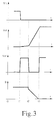
- the variations of some electrical quantities of the circuit of Figure 2 are shown in qualitative time graphs.
- the first graph shows the variation with time of the potential (Vbl) of the terminal Bl
- the second graph shows the variation of the potential (Vch) of the terminal Ch
- the third graph shows the variation of the potential (Vcl') of the internal collector terminal of the transistor Tl (Cl' in Figure 2), all measured relative to earth
- the fourth graph shows the variation of the current through the load L (Il in Figure 2).
- the two switches S1 and S2 are closed, starting the switching stage of the two transistors Tl and Th.
- the potential of the base terminal Bl (Vbl) is brought to zero; upon completion of the turning-off stage of the low-voltage transistor Tl, which is considered negligible in comparison with that of the high-voltage transistor Th, the potential of the internal collector terminal of the transistor Tl (Vcl') is brought to a high value.
- the transistor Tl is turned off, its collector current, which corresponds to the emitter current of the transistor Th, is brought to zero.
- the turn-off time of the high-voltage transistor Th is greater because of the large accumulation of charges in its base region. Consequently, after the transistor Tl has been turned off, bringing the emitter current of the transistor Th to zero, the collector current of the transistor Th flows through its base and the internal resistor Rp', and is discharged to earth through the Zener diode Dz.
- the transistor Th is turned off. Its collector current is brought to zero and the potential of the collector terminal of the transistor Th (Vch) starts to be brought to a high value.
- This variation (dV/dt) of the potential of the terminal Ch generates a transitory phenomenon in the RC network constituted by the capacitors C1 and C2 and by the resistors Rp and Rp'.
- the current Il flows through the capacitor C1 and starts to fall to zero, being discharged to earth through the resistor Rp' and the capacitor C2 and the resistor Rp in series.
- the transitory phenomenon thus generated produces a voltage pulse at the internal base terminal of the transistor Tl (Bl' in Figure 2).
- the NPN transistor Tl and the PNP transistor Tp define an SCR; in particular, the emitter terminal of the transistor Tp constitutes the anode of the SCR, the emitter terminal of the transistor Tl constitutes the cathode, and the internal base terminal of the transistor Tl (Bl') constitutes the control electrode.
- the voltage pulse described above applied to the control electrode of the SCR therefore starts it resulting in conduction between the anode and the cathode.
- the voltage pulse at the internal base terminal of the transistor Tl (Bl') switches on the NPN transistor Tl so that the potential of its internal collector terminal (Vcl') is brought to zero. This switches on the parasitic PNP transistor Tp which is supplied by means of the capacitor C1 and causes the entire power device to be switched on again, with conduction between its terminals El and Ch.
- the SCR structure formed by the transistors T1 and Tp is turned off and the potential of the collector terminal of the transistor Th (Vch) reaches a high value equal to Vcc; the power device is thus brought to the correct turned-off state, completing its switching.
- the anomalous operation of the circuit with the starting of the SCR structure described above depends upon the value of the layer resistance Rp, whereas the duration t3-t2 of the transitory stage depends upon the time constant RC of the circuit constituted by the various parasitic components of the device and, in particular, upon the values of the layer resistances Rp and Rp'.
- the values of the layer resistances Rp and Rp' depend upon the widths of the emitter fingers of the low-voltage transistor. These widths are dictated by current-flow requirements and the robustness of the device and cannot fall below certain values.
- FIG. 4a this is a schematic, perspective view of a portion of an integrated device according to the present invention.
- the integrated device is formed in a chip 400 of semiconductor material comprising an N+ substrate 105 on which a first N-epitaxial layer 110 is formed.
- P-type regions are formed by implantation on the surface of the epitaxial layer 110 and N-type regions are then formed thereon by a subsequent implantation step; a second N-type epitaxial layer 115 is formed thereon by epitaxial growth.
- the implanted P-type and N-type regions described above extend by diffusion in the two epitaxial layers giving rise to buried regions which define P-N junctions.
- a P-type region 405 having a high concentration of impurities is then formed in the second epitaxial layer 115 by known masking and diffusion techniques and extends all the way through the second epitaxial layer 115, so as to be connected to a buried P-type region 120.
- the P-type region constituted by the regions 120 and 405 contains the base region of the high-voltage transistor and delimits a portion of the epitaxial layer 115 which contains the emitter region of the same transistor; the collector region of the high-voltage transistor is contained in the portion of the epitaxial layer 110 and of the substrate 105 disposed between the buried region 120 and the lower surface of the chip.
- the contact region 405 has a network structure such as to divide the emitter region of the high-voltage transistor into a plurality of isolated cells.
- a cell 410 there is a buried N-type region 415 which forms a junction with a portion of the buried P-type region 120.
- N-type region 420 with a high concentration of impurities is then formed by similar implantation techniques (or alternatively by a deposition process) and diffusion techniques and extends in the second epitaxial layer 115; in the embodiment shown in the drawing, this enrichment region 420 extends as far as the respective buried region 415.
- a P-type region 425 is then implanted and diffused by similar techniques, an N-type region 430 being formed therein.
- the N-type region disposed between the buried region 415 and the region 425 contains an elemental collector region of the low-voltage transistor; the P-region 425 and the N-type region 430 contain, respectively, an elemental base region and an elemental emitter region of the same low-voltage transistor.
- the set of various elemental base and emitter regions formed in the various cells of the device (which are interconnected electrically as described in detail below) and the set of various elemental collector regions define the base, emitter and collector regions of the low-voltage transistor, respectively.
- the low-voltage transistor can be seen as being constituted by a plurality of elemental transistors (each formed in a single cell) connected in parallel with one another.
- the cellular structure of the device according to the present invention reduces the layer resistance (Rp) of the base region of the low-voltage transistor and that (Rp') of the base region of the high-voltage transistor as well as the size of the parasitic transistor (Tp) described above, thus reducing the problems encountered in known devices.
- the size of the cell 410 determines the value of the layer resistance Rp' of the base region of the high-voltage transistor and the size of the parasitic transistor Tp.
- the width of the region 425 determines the value of the elemental layer resistance of a single elemental base region of the low-voltage transistor; the total layer resistance Rp is given by these elemental resistances in parallel.
- an increase in the cell size of the network of the structure according to the present invention reduces the effects of the parasitic elements described above.
- this reduction reduces the current-flow of the device as a result of the reduction of the areas of the emitter regions of the two transistors.
- the cell-size selected for the network is therefore a compromise solution between these two contrasting requirements.
- the N-type enrichment region 420 is not strictly necessary. However, this region is useful because increased doping of the base region of the parasitic PNP transistor formed between the P-type region 420, the N-type region of the cell and the P-type region 120, 405 reduces its gain.
- the front surface of the chip 400 is then coated with an insulating layer (not shown in the drawing) in which contact openings are formed by known deposition, masking and etching techniques for the subsequent metallization stage.
- the base electrode (Bh) of the high-voltage transistor and the base and emitter electrodes (Bl and El) of the low-voltage transistor Tl are formed in this stage, as described in detail below.
- a metal layer 185 is formed on the base of the chip, that is, on the free surface of the substrate 105 and constitutes the collector electrode (Ch) of the high-voltage transistor.
- FIG. 4b this is a plan view of the integrated device of Figure 4a before the metallization stage.
- the chip 400 is covered with an insulating layer 150 beneath which the various regions of semiconductor material of the cell 410 described above can be seen.
- the blackened regions represent the contact openings cut in the insulating layer 150.
- a hole 435 which defines a contact region with the base region 405, 120 of the high-voltage transistor can be seen; this hole 435 has a network structure which is broken to allow each cell to be connected to at least one adjacent cell by a single layer of metallization (as described in detail below).
- a cell can be connected to two adjacent cells; this allows the various cells to be connected such that each cell is connected to a preceding cell and to a following cell, except for the first and last cells which are connected to a single adjacent cell.
- openings 440, 441 and 445 which define regions for contact with the base region 425 and with the emitter region 430 of the low-voltage transistor, respectively. It should be noted that, in the embodiment of the present invention shown in the drawing, two separate contact openings 440 and 441 are provided for the base region 425; this measure further reduces the distributed layer resistance between the base region of the low-voltage transistor and the corresponding base terminal.
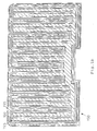
- FIG. 4c is a plan view of the entire device before the metallization stage.
- the network structure of the deep base contact region of the high-voltage transistor and the broken network structure of the corresponding contact hole can be seen therein; the various cells in which the various elemental low-voltage transistors are formed are thus visible.
- FIG. 4d this is a plan view of the integrated device of Figure 4c, after the metallization stage.
- a metal strip 450 in contact with the base region 405, 120 of the high-voltage transistor through the hole 435) which defines its base electrode (Bh)
- metal strips 455 and 460 in contact with the base and emitter regions 425 and 430 of the low-voltage transistor, respectively, through the openings 440, 441 and 445) which define the base electrode (Bl) and the emitter electrode (El) of the low-voltage transistor, respectively.
- the metal strip 450 is constituted by a main element (comprising the base electrode Bh of the high-voltage transistor) from which a plurality of substantially parallel, elongate, herring-bone-shaped metallization elements extend perpendicularly; this shape improves contact with the base region of the high-voltage transistor Th.
- the base electrode Bl of the low-voltage transistor is formed in a separate region from the power device and contacts the various elemental base regions of the low-voltage transistor Tl in the most extensive possible manner by means of the metal strip 455.
- this embodiment of the present invention achieves the necessary connections between the various regions with a single metallization layer. Experts in the art will appreciate that the same result can also be achieved by different geometry if the network structure of the hole 435 is broken at different points from those shown in the drawing. Alternatively, it is, of course, possible to use a closed network structure for the hole 435 without break points, the contacts between the elemental base and emitter regions of the individual cells being formed by means of a second metallization layer.
Landscapes
- Bipolar Integrated Circuits (AREA)
Priority Applications (3)
| Application Number | Priority Date | Filing Date | Title |
|---|---|---|---|
| EP96830306A EP0810662A1 (fr) | 1996-05-29 | 1996-05-29 | Dispositif intégré à configuration de commutateur à émetteur et avec une structure cellulaire |
| US08/864,653 US6084286A (en) | 1996-05-29 | 1997-05-28 | Integrated device in an emitter switching configuration and with a cellular structure |
| JP9139940A JPH1056073A (ja) | 1996-05-29 | 1997-05-29 | エミッタスイッチング構成における、セル状構造を有する集積装置 |
Applications Claiming Priority (1)
| Application Number | Priority Date | Filing Date | Title |
|---|---|---|---|
| EP96830306A EP0810662A1 (fr) | 1996-05-29 | 1996-05-29 | Dispositif intégré à configuration de commutateur à émetteur et avec une structure cellulaire |
Publications (1)
| Publication Number | Publication Date |
|---|---|
| EP0810662A1 true EP0810662A1 (fr) | 1997-12-03 |
Family
ID=8225919
Family Applications (1)
| Application Number | Title | Priority Date | Filing Date |
|---|---|---|---|
| EP96830306A Ceased EP0810662A1 (fr) | 1996-05-29 | 1996-05-29 | Dispositif intégré à configuration de commutateur à émetteur et avec une structure cellulaire |
Country Status (3)
| Country | Link |
|---|---|
| US (1) | US6084286A (fr) |
| EP (1) | EP0810662A1 (fr) |
| JP (1) | JPH1056073A (fr) |
Cited By (1)
| Publication number | Priority date | Publication date | Assignee | Title |
|---|---|---|---|---|
| EP0847597A1 (fr) * | 1996-06-28 | 1998-06-17 | Pac Tech - Packaging Technologies GmbH | Procede de configuration d'un systeme spatial de puces et systeme spatial de puces correspondant |
Citations (3)
| Publication number | Priority date | Publication date | Assignee | Title |
|---|---|---|---|---|
| US3772100A (en) * | 1971-06-30 | 1973-11-13 | Denki Onkyo Co Ltd | Method for forming strips on semiconductor device |
| EP0493854A1 (fr) * | 1990-12-31 | 1992-07-08 | STMicroelectronics S.r.l. | Structure intégrée d'un transistor de puissance et d'un transistor à basse-tension dans une configuration à commutation d'émetteur ou semi-pont et procédés de fabrication associés |
| US5399899A (en) * | 1992-12-28 | 1995-03-21 | U.S. Philips Corporation | Bipolar epitaxial cascode with low-level base connection |
Family Cites Families (3)
| Publication number | Priority date | Publication date | Assignee | Title |
|---|---|---|---|---|
| IT1217322B (it) * | 1987-12-22 | 1990-03-22 | Sgs Microelettronica Spa | Procedimento di fabbricazione di un dispositivo nonolitico a semiconduttope comprendente almeno un transistor di un circuito integrato di comando e un transistor di rotenza in tegrato nella stessa piastrina |
| US5204735A (en) * | 1988-04-21 | 1993-04-20 | Kabushiki Kaisha Toshiba | High-frequency semiconductor device having emitter stabilizing resistor and method of manufacturing the same |
| US5631495A (en) * | 1994-11-29 | 1997-05-20 | International Business Machines Corporation | High performance bipolar devices with plurality of base contact regions formed around the emitter layer |
-
1996
- 1996-05-29 EP EP96830306A patent/EP0810662A1/fr not_active Ceased
-
1997
- 1997-05-28 US US08/864,653 patent/US6084286A/en not_active Expired - Lifetime
- 1997-05-29 JP JP9139940A patent/JPH1056073A/ja active Pending
Patent Citations (3)
| Publication number | Priority date | Publication date | Assignee | Title |
|---|---|---|---|---|
| US3772100A (en) * | 1971-06-30 | 1973-11-13 | Denki Onkyo Co Ltd | Method for forming strips on semiconductor device |
| EP0493854A1 (fr) * | 1990-12-31 | 1992-07-08 | STMicroelectronics S.r.l. | Structure intégrée d'un transistor de puissance et d'un transistor à basse-tension dans une configuration à commutation d'émetteur ou semi-pont et procédés de fabrication associés |
| US5399899A (en) * | 1992-12-28 | 1995-03-21 | U.S. Philips Corporation | Bipolar epitaxial cascode with low-level base connection |
Non-Patent Citations (1)
| Title |
|---|
| ANONYMOUS: "Bipolar Transistor Structure. July 1978.", IBM TECHNICAL DISCLOSURE BULLETIN, vol. 21, no. 2, July 1978 (1978-07-01), NEW YORK, US, pages 846 - 849, XP002016733 * |
Cited By (1)
| Publication number | Priority date | Publication date | Assignee | Title |
|---|---|---|---|---|
| EP0847597A1 (fr) * | 1996-06-28 | 1998-06-17 | Pac Tech - Packaging Technologies GmbH | Procede de configuration d'un systeme spatial de puces et systeme spatial de puces correspondant |
Also Published As
| Publication number | Publication date |
|---|---|
| JPH1056073A (ja) | 1998-02-24 |
| US6084286A (en) | 2000-07-04 |
Similar Documents
| Publication | Publication Date | Title |
|---|---|---|
| JP3911566B2 (ja) | Mos型半導体装置 | |
| US5536958A (en) | Semiconductor device having high voltage protection capability | |
| KR0169552B1 (ko) | 전계효과형 반도체 장치 및 그 제조방법 | |
| US4721986A (en) | Bidirectional output semiconductor field effect transistor and method for its maufacture | |
| US4755697A (en) | Bidirectional output semiconductor field effect transistor | |
| KR920005539B1 (ko) | 정확히 설정된 동작전압을 갖는 반도체 과전압 억제기 및 그의 제조방법 | |
| EP0646965A1 (fr) | Un dispositif intégré avec un transistor bipolaire et un transistor MOSFET dans une configuration à commutation d'émetteur | |
| KR19990026902A (ko) | 정전기 보호회로 | |
| EP0314465B1 (fr) | Dispositif semi-conducteur avec un MOSFET vertical de puissance isolé. | |
| EP0215493B1 (fr) | Circuit à transistors MOS protégé | |
| KR100275758B1 (ko) | 제너 다이오드를 내장한 수평형 모스 게이트형 반도체 소자 및그 제조 방법 | |
| EP0629001B1 (fr) | Structure monolithique intégré d'un transistor bipolaire vertical et d'un transistor MOSFET vertical | |
| ATE107440T1 (de) | Monolithisch integrierbare transistorschaltung zum begrenzen von positiver überspannung. | |
| EP0625797B1 (fr) | Structure intégrée d'une résistance de détection de courant pour les dispositifs MOS à puissance, en particulier pour les dispositifs MOS à puissance autoprotégés contre la surcharge | |
| EP1469523B1 (fr) | Composant électronique de jonction et dispositif de puissance intégrée comportant ce composant | |
| US3427512A (en) | Semiconductor low voltage switch | |
| EP0493854B1 (fr) | Structure intégrée d'un transistor de puissance et d'un transistor à basse-tension dans une configuration à commutation d'émetteur ou semi-pont et procédés de fabrication associés | |
| EP1022785B1 (fr) | Dispositif electronique semi-conducteur de puissance avec diode intègrèe | |
| EP0680089A1 (fr) | Dispositif semi-conducteur de puissance comprenant une structure de circuit intégré de protection contre des surtensions, et procédé de fabrication associé | |
| EP0632505B1 (fr) | Transistor bipolaire vertical à puissance avec une base enterrée et une géométrie interdigitée | |
| US6127723A (en) | Integrated device in an emitter-switching configuration | |
| US6084286A (en) | Integrated device in an emitter switching configuration and with a cellular structure | |
| EP0624906B1 (fr) | Structure de circuit intégré pour la protection de dispositifs de puissance contre des surtensions | |
| EP0225586A1 (fr) | Circuit de protection contre les surtensions pour un dispositif MOS intégré | |
| EP0810503B1 (fr) | Un circuit intégré avec un dispositif ayant un seuil de conduction inverse prédéterminé et un dispositif de compensation thermique avec multiplicateurs de Vbe |
Legal Events
| Date | Code | Title | Description |
|---|---|---|---|
| PUAI | Public reference made under article 153(3) epc to a published international application that has entered the european phase |
Free format text: ORIGINAL CODE: 0009012 |
|
| 17P | Request for examination filed |
Effective date: 19970424 |
|
| AK | Designated contracting states |
Kind code of ref document: A1 Designated state(s): DE FR GB IT |
|
| 17Q | First examination report despatched |
Effective date: 19981113 |
|
| STAA | Information on the status of an ep patent application or granted ep patent |
Free format text: STATUS: THE APPLICATION HAS BEEN REFUSED |
|
| 18R | Application refused |
Effective date: 20010920 |