EP0811862A2 - Système d'interconnection optique carte-à-carte et unité-à-unité - Google Patents
Système d'interconnection optique carte-à-carte et unité-à-unité Download PDFInfo
- Publication number
- EP0811862A2 EP0811862A2 EP97108914A EP97108914A EP0811862A2 EP 0811862 A2 EP0811862 A2 EP 0811862A2 EP 97108914 A EP97108914 A EP 97108914A EP 97108914 A EP97108914 A EP 97108914A EP 0811862 A2 EP0811862 A2 EP 0811862A2
- Authority
- EP
- European Patent Office
- Prior art keywords
- array
- optical
- deflection control
- interconnection system
- devices
- Prior art date
- Legal status (The legal status is an assumption and is not a legal conclusion. Google has not performed a legal analysis and makes no representation as to the accuracy of the status listed.)
- Granted
Links
Images














Classifications
-
- G—PHYSICS
- G02—OPTICS
- G02B—OPTICAL ELEMENTS, SYSTEMS OR APPARATUS
- G02B6/00—Light guides; Structural details of arrangements comprising light guides and other optical elements, e.g. couplings
- G02B6/24—Coupling light guides
- G02B6/42—Coupling light guides with opto-electronic elements
- G02B6/43—Arrangements comprising a plurality of opto-electronic elements and associated optical interconnections
Definitions
- Sakano et al. with the NTT have accomplished the 20 Mbit/s neighboring board free-space optical interconnection system, though low density and low speed, in which four sheets of the boards on which 4 ⁇ 4 LEDs and detectors are mounted are arranged (T. Sakano, T. Matsumoto, and K. Noguchi; "Three-Dimensional Board-to-Board Free-Space Interconnections and Their Application to the Prototype Multiprocessor System: COSINE- ", Applied Optics, vol.34, pp.1815-1822, 1995).
- the optical beam emitted from the transmitter array is input into the polarization beam splitter, and then turned by a right angle to input the opening portion of the board in succeeding stage. Then, polarization of the optical beam is controlled by the polarization control array device provided on the opening portion to thereby rotate a plane of polarization by 90° , then the optical beam is turned by the polarization beam splitter by a right angle to input into the light deflection control array device which then controls the propagation direction of the optical beam to input into the desired photodetector.
- the optical beam whose plane of polarization is not rotated by the polarization control array device by 90° passes through the polarization beam splitter along the propagation direction to input into the opening portion of the board in succeeding stage, and is then controlled similarly.
- the transmitter arrays and the detector arrays are provided vertically with the board.
- the transmitter arrays include beam array batch deflection control devices which deflect collectively the optical beam array output.
- the first light deflection control array devices and the second light deflection control array devices are composed respectively of a liquid crystal prism array in which two sheets of liquid crystal prism arrays are stuck orthogonally.
- the first light deflection control array devices and the second light deflection control array devices are composed respectively of a rotation prism array in which beam propagation directions can be controlled mechanically.
- the beam array batch deflection control device is formed of a variable apex angle prism.
- the transmitter arrays include vertical cavity surface emitting laser diode (VCSEL) arrays for emitting the optical beam array respectively.
- VCSEL vertical cavity surface emitting laser diode
- an optical interconnection system applied to a cabinet in which a plurality of boards on each of which electronic circuits are mounted are assembled like a book shelf by supporting members to constitute units and then plural units are stuck in a direction parallel with the boards
- the optical interconnection system comprising: transmitter arrays provided on boards in at least preselected stages in respective units, for outputting an optical beam array; light deflection control array devices for controlling individually propagation directions of respective optical beams of the optical beam array emitted from the transmitter arrays; output prism mirrors for turning the optical beam array emitted from the light deflection control array devices by a right angle; input prism mirrors provided on respective boards in succeeding stage to the boards on which the transmitter arrays are provided, for turning the optical beam array, which is emitted from the output prism mirrors in other units, by a right angle to direct to corresponding boards; and detector arrays composed of a plurality of detectors to receive the optical beam array emitted from the input prism mirrors; and wherein the
- the board-to-board free-space optical interconnection system between the boards in a certain unit and a different unit arbitrarily can be established freely by introducing the light deflection control array device which is capable of controlling the propagation direction of the optical beam.
- the units can be connected by images in place of the optical beam.
- an optical interconnection system applied to a cabinet in which a plurality of boards on each of which electronic circuits are mounted are assembled like a book shelf by supporting members to constitute units and then plural units are stuck in a direction parallel with the boards
- the optical interconnection system comprising: transmitter arrays provided on boards in at least preselected stages in respective units, for outputting an optical beam array; light deflection control array devices for controlling individually propagation directions of respective optical beams of the optical beam array emitted from the transmitter arrays; polarization control array devices provided to correspond to respective boards in at least preselected stages, for controlling polarization directions of respective optical beams in the optical beam array emitted from remaining units; polarization beam splitters provided close to the propagation control array devices, for receiving the optical beam array emitted from corresponding light deflection control array devices and then turning by a right angle to direct to remaining units, and directing the optical beam array, which is input from the other units via the polarization control array devices, straight to the other units or
- the preferred embodiment of the present invention further comprises fixed-angle light deflection devices which deflect fixedly and individually propagation directions of respective optical beams in the optical beam array emitted from the transmitter arrays.
- the light deflection control array devices are composed of a liquid crystal prism array in which two sheets of liquid crystal prism arrays are stuck orthogonally.
- the light deflection control array devices are composed of a liquid crystal deflection control array device in which a liquid crystal layer is sandwiched by array split electrodes having a window therein.
- the light deflection control array devices are composed of an electrostatic control micro mirror array in which beam propagation directions can be controlled by an electrostatic force.
- the light deflection control array devices are composed of a hologram in which a diffraction grating can be written.
- the light deflection control array devices are composed of a rotation mirror array in which beam propagation directions can be controlled mechanically.
- the fixed-angle deflection device is formed of a hologram, a prism array, or a mirror array.
- the beam array batch deflection control device is formed of a variable apex angle prism.
- the beam array batch deflection control device is formed of a liquid crystal prism array in which two liquid crystal prism arrays are orthogonally stuck.
- the preferred embodiment of the present invention further comprises: a monitor beam VCSEL included in the transmitter arrays, for emitting a monitor beam; a position sensor included in the receiver arrays, for receiving the monitor beam via the light deflection control array devices, the beam array batch deflection control device, the output prism mirror, and the input prism mirror to detect its position; and a feedback circuit for controlling the beam array batch deflection control devices in response to the position of the monitor beam detected by the position sensor.
- the preferred embodiment of the present invention further comprises: a monitor beam VCSEL included in the transmitter arrays, for emitting a monitor beam; a position sensor included in the receiver arrays, for receiving the monitor beam via the light deflection control array devices, the beam array batch deflection control device, the output prism mirror, the macro lens, and the input prism mirror to detect its position; and a feedback circuit for controlling the beam array batch deflection control devices in response to the position of the monitor beam detected by the position sensor.
- the preferred embodiment of the present invention further comprises: a monitor beam VCSEL included in the transmitter arrays, for emitting a monitor beam; a position sensor included in the receiver arrays, for receiving the monitor beam via the light deflection control array devices, the beam array batch deflection control device, the polarization control array devices, and the polarization beam splitters to detect its position; and a feedback circuit for controlling the beam array batch deflection control devices in response to the position of the monitor beam detected by the position sensor.
- the light deflection control array devices are composed of a liquid crystal microprism array in which a liquid crystal is sandwiched by a planar substrate and a microprism array plate having transparent electrodes and alignment layer thereon.
- the light deflection control array devices are composed of a hologram in which a diffraction grating can be written.
- the preferred embodiment of the present invention further comprises: a monitor beam VCSEL included in the transmitter arrays, for emitting a monitor beam; a position sensor included in the receiver arrays, for receiving the monitor beam via the light deflection control array devices and the mirror to detect its position; and a feedback circuit for controlling the beam array batch deflection control devices in response to the position of the monitor beam detected by the position sensor.
- second mirrors are placed on an outside of one outermost board of the first board group being boards assembled like a book shelf along an optical beam propagation direction at an angle non-parallel with first mirrors serving as the mirrors, and a spatial alignment of the second mirrors is determined such that the optical beams reaching the second mirrors are reflected to re-input into the first mirror and then the optical beams are input into the detector arrays mounted on second board groups inserted between the boards of the first board group like the book shelf.
- third mirrors are placed on an outside of other outermost board opposite to one outermost board of the first and second board groups being boards assembled like a book shelf at an angle non-parallel with first mirrors, and a spatial alignment of the third mirrors is determined such that the optical beams reaching the third mirrors after reflected by the second mirrors are reflected to re-input into the first mirror and then the optical beams are input into the detector arrays mounted on third board group inserted between the boards of the first and second board groups like the book shelf.
- FIG.7 although only the optical beams emitted from the leftmost board are illustrated on account of limited space, actually the optical beams are similarly emitted from all of the boards 2-1. Also, in FIG.7, although only the foremost optical beam is illustrated on account of space consideration, actually plural optical beams must be depicted along the inside direction perpendicular to the sheet. The optical beams are emitted from all the boards obliquely in the right downward direction. The directions of the optical beams are then controlled by the light deflection control array device to thus make it possible to achieve complicated cross optical interconnections.
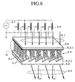
- FIG.8 is a view showing a detailed configuration of the LC microprism array 7-4 serving as the light deflection control array device which is used in the board-to-board optical interconnection system shown in FIG.7.
- This LC microprism array is set forth in a literature, for example, K. Hirabayashi, T. Yamamoto, and M. Yamaguchi; "Free-Space Optical Interconnections with Liquid Crystal Microprism Arrays", Applied Optics, vol.34, pp.2571-2580, (1995).
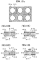
- an LC deflection device there is an LC deflection device.
- the array device has such a configuration that an LC layer is sandwiched by split electrodes having a window therein.
- a refractive index distribution is provided to the LC layer by controlling the voltage applied to the split electrodes to thus deflect the optical beam up to about 10 degrees.
- deflection directions of individual optical beams can be controlled.
- FIGS.10A to 10E A configuration of the LC deflection array device is shown in FIGS.10A to 10E.
- FIG.10A is a top view of the LC deflection device
- FIGS.10B to 10E are sectional views of the LC deflection device.
- 10-1a, 10-1b, 10-1c, 10-1d are Al electrodes; 10-2, a glass substrate; 10-3, an LC layer; 10-4, an incident light; and 10-5, an output light.
- the LC assumes homeotropic alignment which is directed perpendicular to the substrate.
- a polarity of the voltage applied to the Al electrodes 10-1a to 10-1d is changed to + and -, an alignment distribution of liquid crystal molecules is changed.
- the refractive index distribution is changed to thereby deflect the incident optical beam.
- FIGS. 10B to 10E illustrate behaviors of the optical beam deflection if the voltage applied to the Al electrodes 10-1a to 10-1d is changed to + and -.
- the propagation direction of the optical beam can be controlled by varying polarity and magnitude of the voltage applied to respective electrodes.
- polarity and magnitude of the voltage applied to respective electrodes See a literature, A. Sasaki and T. Ishibashi; “Liquid-Crystal Light Deflector”, Electronics Lett., vol.10 (1979), pp.293-294.
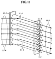
- FIGS. 11 and 12 Configurations of the rotation prism array and the rotation mirror array are shown in FIGS. 11 and 12 respectively.
- 11-1 denotes a microprism column
- 11-2 a frame for holding the microprism column 11-1
- 11-3 a screw for rotating the microprism column 11-1
- 11-4 a group of incident optical beams
- 11-5 a group of refracted optical beams.
- the propagation direction of the refracted optical beams can be controlled by adjusting rotation of respective microprism columns 11-1.
- FIGS.14A, 14B, and 14C the results of performance evaluation are shown in FIGS.14A, 14B, and 14C under the conditions that a distance between the mirror and the board end is set to 30mm, a range of a tunable deflection angle of the light deflection control array device is selected within 5 degrees (which corresponds to the case where an apex angle of the LC microprism array is selected to 20° ), and a pitch of the array is set to 1mm.
- FIG.14A is a view illustrating relationships between an output angle and maximum and minimum propagation distances.
- FIG.14B is a view illustrating a relationship between the output angle and the number of boards which can be interconnected.
- the fixed-angle prism array 15-1 is so designed that apex angles are refracted correspondingly to the optical interconnection of individual optical beams.
- FIG.16 is a perspective view showing a configuration of a board-to-board optical interconnection system according to a fourth embodiment of the present invention.
- FIG.17 is a sectional view showing the configuration of the board-to-board optical interconnection system in FIG.16.
- a special mount is required so that various troubles are caused upon mounting the special mount on the board.
- the board-to-board optical interconnection system shown in FIGS.16 and 17 is constituted such that the VCSEL array 7-1, the lens array 7-2, and the LC microprism array 7-4 can be mounted on the board in parallel with the board, whereby various troubles can be overcome.
- a device for feeding back location information is provided in order to eliminate total location displacement of the optical beam group.
- the VCSEL 7-1, the lens array 7-2, and the crossed pairs of LC micro prism arrays 16-1 can be assembled in parallel with the board.
- a tapered glass substrate is employed on a back surface of the LC microprism array, so that the optical beam can be refracted obliquely and downward and emitted.
- the LC microprism array has been employed in the optical interconnection.
- one of the micro mirror array, the LC deflection device, the rotation mirror array, and the rotation prism array may be used as the tunable light deflection control array device.
- one of the hologram device, the prism array device, and the mirror array device may be used as the fixed-angle deflection control device.
- one of the LC prism array, the micro mirror array, the LC deflection device, the rotation mirror array, and the rotation prism array may be used as the tunable light deflection control array device.
- a combination of the fixed-angle deflection control device and the tunable light deflection control array device may of course be used.
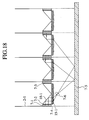
- FIG.18 is a view showing a configuration of a board-to-board optical interconnection system according to a fifth embodiment of the present invention.
- a prism mirror 18-1 is provided to assemble the VCSEL and the lens array, which have been explained in the first embodiment shown in FIG.7, in parallel with the board, and also an LC microprism array 7-4 for the purpose of correction and a fixed-angle prism array 15-1 are provided on a lower surface of the prism mirror 18-1.
- the fixed-angle prism array has been used mainly in the optical interconnection and the LC microprism array has been used auxiliarily.
- the micro mirror array, the LC deflection device, the rotation mirror array, and the rotation prism array may be used selectively as the tunable light deflection control array device.
- one of the prism array, the hologram device, and the prism array device may be used as the fixed-angle deflection control device.
- one of the LC prism array, the micro mirror array, the LC deflection device, the rotation mirror array, and the rotation prism array may be used as the tunable light deflection control array device.
- a combination of the fixed-angle deflection control device and the tunable light deflection control array device may be used.
- FIG.19A is a view showing a configuration of a board-to-board optical interconnection system according to a sixth embodiment of the present invention.
- a second mirror 19-4 is provided on the outside of the outermost board of the board group along the propagation direction of the optical beam, and then the optical beam is reflected by the second mirror 19-4 to input into respective photodetector arrays of the second board group.
- 19-1 denotes a first board group
- 19-2 a second board group
- 19-3 a first mirror placed horizontally
- 19-4 a second mirror placed substantially perpendicular to the first mirror 19-3
- 19-5 an optical beam group to connect the first board group 19-1
- 19-6 an optical beam group reflected by the second mirror 19-4 to connect the second board group 19-2.
- the optical beam proceeds while being reflected by the first board group 19-1 and the first mirror 19-3, then is reflected by the second mirror 19-4, and then returns to proceed in the opposite direction while being reflected by the second board group 19-2 interposed between the first board group 19-1 and the first mirror 19-3.
- the optical beam interconnection can be utilized when the optical beam propagates in the reverse direction.
- FIG.20 is a perspective view showing a configuration of a board-to-board optical interconnection system according to a seventh embodiment of the present invention.
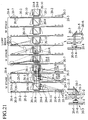
- FIG.21 is a side sectional view showing the configuration of the board-to-board optical interconnection system in FIG.20.
- a plurality of boards 20-0 on which a great number of electronic parts such as very high speed, super high density and large capacity LSIs, e.g., switch LSIs 20-2, are mounted are assembled in substantially parallel like a book shelf and then optical signals are transmitted and received between the plurality of boards 20-0.
- Window portions 20-1 serving as opening areas are formed in substantially central areas of respective boards 20-0 to transmit the optical beams to plural boards respectively therethrough and the optical beams can be transmitted to respective boards through these window portions.
- transmitter arrays 20-3 for transmitting the optical beam arrays are provided to the lowermost portions of respective boards.
- Receiver arrays 20-4 for receiving the optical beams are provided on the uppermost portions of respective boards.
- 20-0 denotes a board; 20-1, a window portion formed in the central area of the board; 20-2, a switch LSI mounted on the board 20-0; 20-3, a transmitter array having a transmitter array with a lens array and a second light deflection control array device as a unit; 20-4, a receiver array used as a photodetector array with the lens array; 20-5, an electric connector; 20-6, an optical beam array output from the transmitter array 20-3; and 20-7, a prism mirror for turning the optical beam at a right angle.
- 20-8 denotes a twisted nematic (TN) LC array device used as a polarization controller; 20-9, a polarization beam splitter (abbreviated as PBS hereinafter); 20-10, an LC microprism array used as first light deflection control array devices which sandwiches the polarization beam splitter 20-9 vertically; and 20-11, an optical beam array output from the PBS 20-9 upwardly.
- TN twisted nematic
- FIG.21 shows detailed configurations of the transmitter array 20-3 and the receiver array 20-4 as a partially enlarged sectional view.
- 21-1 denotes a VCSEL array used as a light source; 21-2, a lens array; 21-3, an LC microprism array used as a second light deflection array device; 20-7, a prism mirror; 21-5, an optical beam; 21-8, a photodetector array; 21-6, a solder bump for mounting the VCSEL array 21-2 and the photodetector array 21-8; and 20-0, a board.
- a mark ⁇ represents a polarization perpendicular to a surface of the sheet
- a mark ⁇ represents a polarization parallel with the surface of the sheet.
- the light deflection control array device for deflecting the optical beam is composed of the LC microprism array as shown in FIG.8, for example, like the first embodiment.
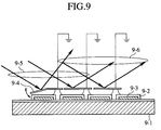
- the micro mirror array shown in FIG.9, the LC deflection device shown in FIG.10, the rotation prism array shown in FIG.11, and the mechanical rotation mirror shown in FIG.12 may be used like the first embodiment.
- the light deflection device selected from a group of the prism array, the hologram array, and the mirror array whose profiles are fixed may be used in the event that the optical interconnections are previously arranged.
- similar advantages can be expected if the fixed-angle light deflection device and the tunable type light deflection control array device, as mentioned above, are combined together arbitrarily.
- the optical beam 21-5 is emitted from the VCSEL array 21-1 of the transmitter array 20-3 positioned on the lowermost portion of the board 20-0, then deflected by the LC microprism array 21-3 used as the second light deflection array device, and then turned by the prism mirror 20-7 by a right angle to select the position of the LC prism (the microprism formed of the transparent substrate 8-2-2 shown in FIG.8) in the lower LC microprism array 20-10 used as the first light deflection control array device.
- the optic axis of the optical beam 20-6 can be adjusted by the LC prism so as to input perpendicularly to the PBS 20-9.
- the optical beam 20-6 is then turned by the PBS 20-9 by a right angle to proceed the neighboring board 20-0.
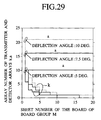
- the number of the transmitter array and the detector array both can be mounted on the board, are calculated under the assumption that a length of the board 20-0 is 30cm, a size of the polarization beam splitter 20-9 is 20mm square, an apex angle of the LC microprism array 20-10 is 20° , 30° , 40° , and a deflection angle is 5 , 7.5° , 10° .
- the PBS 20-9 with 20mm square is placed in the center of the board 20-0, and the LC microprism array 20-10 serving as the first light deflection control array device includes L arrays with 1mm pitch and is stuck on the PBS 20-9 to coincide its top end with the end of the PBS 20-9. It is also assumed that the prism mirror mounted on the laser array and the detector array has a size of 1mm square.
- FIGS.23 to 25 relationships between the length and the array numbers k , a of the LC microprism array and the array distance are shown in FIGS.23 to 25. Further, the total results of FIGS.23 to 25 are shown in FIG.26.
- the deflection angle of the LC prism is 5°
- the array number of the LC microprism array and the array numbers k a of the detector array can be given as 9 and 3, 5 respectively as optimal values, and at that time the array pitch is 6.7mm.
- the sheet number M of the board group can be given as 3.
- the array number of the LC microprism array and the array numbers k , a of the detector array can be given as 12 and 4, 7 respectively as optimal values, and at that time the array pitch is 7.7mm.
- the array number of the LC microprism array and the array numbers k a of the detector array can be given as 16 and 4, 9 respectively as optimal values, and at that time the array pitch is 10mm.
- the sheet number M of the board group can be given as 4.
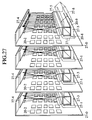
- FIG.27 is a perspective view showing a configuration of the board-to-board optical interconnection system of the eighth embodiment.
- FIGS.28A and 28B are a side sectional view and a front view showing respectively the configuration of the board-to-board optical interconnection system of the eighth embodiment.
- the board-to-board optical interconnection system of the eighth embodiment is constructed such that the transmitter array and the photodetector array are mounted vertically to the board. Therefore, in contrast to the seventh embodiment shown in FIGS. 20 and 21 wherein the transmitter array and the photodetector array are mounted parallel to the board, a higher package density can be achieved.
- 27-0 denotes a board; 20-2, a switch LSI; 27-3, a transmitter array made of a light source array with a lens array; 27-4, a receiver array used as a detector array with a lens array; 27-5, an LC microprism array used as a first light deflection control array device; 20-9, a PBS; 20-8, a TN LC array device used as a polarization control array device; 27-8, an optical beam array; 21-1, a VCSEL array used as a transmitter array; 21-2, a lens array; and 21-8, a photodetector array.
- the mark ⁇ represents a polarization perpendicular to the surface of the sheet, and the mark ⁇ represents a polarization parallel with the surface of the sheet.
- the VCSEL array 21-1 and the lens array 21-2, which constitute the transmitter array 27-3, are mounted vertically on the lower portion of the board 27-0 and the PBS 20-9 is placed over the transmitter array 27-3.
- a collimated beam array emitted from the VCSEL array 21-1 is turned by the PBS 20-9 to propagate rightward.
- the optical beam proceeds upwardly.
- the LC microprism array 27-5 controls the propagation direction of the optical beam.
- This eighth embodiment of the present invention is superior to the seventh embodiment shown in FIGS.20 and 21 in that a pitch of the photodetector array 21-3 can be set to 1mm since the photodetector array 21-3 is mounted vertically on the board and that an area to which the optical beam is allocated can be increased since a propagation distance of the optical beam emitted from the PBS 20-9 over the board can be extended approximately two times.
- the crossed pair of LC prism arrays with an apex angle of 40° can deflect the optical beam within an angle range of ⁇ 5° along two axes, the optical beam can be swung arbitrarily in a 21mm ⁇ 21mm region.
- an unused region of the VCSEL array 21-1 remains even if the cells are mounted at a pitch of 1mm in the 10mm ⁇ 10mm region.
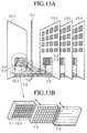
- FIG.30 is a perspective view showing a configuration of the board-to-board optical interconnection system according to the ninth embodiment.
- FIG.31 is a side sectional view showing the configuration of the board-to-board optical interconnection system in FIG.30.
- FIG.32 is a front view showing the configuration of the board-to-board optical interconnection system in FIG.30.
- the transmitter array and the photodetector array are mounted on the board not vertically but parallel with the board in contrast to the board-to-board optical interconnection system explained with reference to FIGS.27, 28A, 28B, and the prism mirror is mounted on the transmitter array and the photodetector array to turn the optical beam at a right angle.
- the board-to-board optical interconnection system shown in FIGS.30 to 32 becomes similar in configuration to the board-to-board optical interconnection system shown in FIGS.27, 28A, 28B.
- a function of correcting the location displacement of the overall optical beam group is similar to that of the fourth embodiment.
- a dedicated monitor beam MB is output from the transmitter array 30-1 to correct the location displacement.
- This monitor beam MB then reaches the x-y position sensor 30-4 via the prism mirror 30-3, the PBS 20-9, etc.
- the x-y position sensor 30-4 detects a displacement amount between a position to which the monitor beam MB actually propagates and a desired position to which the monitor beam MB has to propagate and a direction between both positions, and then sends such information to the feedback circuit.
- the feedback circuit then controls the transmitter array 30-1 to reduce the displacement amount to zero.
- the present invention is not restricted to the switch boards. But the present invention may be applied similarly to board-to-board interconnection in the computer, etc.
- the explanation has been made with the use of the LC microprism array as the light deflection control array device, but the present invention is not limited to this case.
- similar advantages can be achieved if an LC prism array in which two LC prism arrays are stuck orthogonally via a ⁇ /2 plate, an LC deflection control array device in which an LC layer is sandwiched by array split electrodes having windows therein, an electrostatic control micro mirror array in which directions are controlled by virtue of electrostatic forces individually, a spatial light modulator using an LC display in which a diffraction grating can be written, a rotation mirror array whose direction can be controlled mechanically, and a rotation prism array whose direction can be controlled mechanically are employed.
- the light deflection control array device in which deflection of the optical beam can be controlled in the arbitrary direction has been used, a light deflection device selected from the group of the fixed-angle prism array, the mirror array, and the hologram array may be employed if the optical interconnection has been decided beforehand.
- the tunable light deflection control device in which the above light deflection angle can be set arbitrarily and the fixed-angle light deflection control device in which the light deflection angle is fixed may be combined together.
- a large light deflection angle can be set in the fixed-angle light deflection control device while the tunable light deflection control device can control a small light deflection angle. Therefore, if the former is used as a main deflection device and the latter is used as a fine controlling deflection device, freer optical interconnection can be established.
- the optical beam array emitted from the transmitter array with the lens array which is attached to the lower end portion of the board is received by the light deflection control array device, then the propagation direction of the optical beam array is variably controlled every optical beam to be input into the mirror with a gradient, and then the optical beam array reflected by the mirror is received by the photodetector with the lens array. Therefore, unlike the prior art, it is not requested to control precisely the wavelength of the light source, and the board-to-board free-space optical interconnection can attained by virtue of low cost and precise beam alignment to pass through the optical beam from the desired board to the photodetector mounted on another desired board.
- the light deflection control array device is composed of a combination of the fixed-angle control array device in which the deflection direction is determined previously and the tunable control array device in which the deflection direction is tunable, it is not requested for the optical beam to be considerably deflected in the tunable control array device, so that the prism substrate with a small apex angle can be employed to thus accelerate a response rate.
- the second and/or third mirrors are placed on the outside of one and/or the other outermost board of the first board group, then the optical beam is reflected by the mirror to input into the first mirror once again, and then the optical beam is incident into the photodetector array with the lens array of the second and/or third board groups mounted between the boards of the first board group like the book shelf. Therefore, the package density of the board can be increased.
- the optical beam emitted from the transmitter array is input into the polarization beam splitter, and then turned by a right angle to input the opening portion of the neighboring board. Then, polarization of the optical beam is controlled by the polarization control array device provided on the opening portion to thereby rotate a polarization by 90° , then the optical beam is turned by the polarization beam splitter by a right angle to input into the first light deflection control array device which then controls the propagation direction of the optical beam to input into the desired photodetector.
- the optical beam whose polarization is not rotated by the polarization control array device by 90° passes through the polarization beam splitter along the propagation direction to input into the opening portion of the neighboring board, and is then controlled similarly. Therefore, unlike the optical interconnection using the D fibers in the prior art, the optical interconnection of the present can be established with small loss, small crosstalk, at low cost, and without the intermediate amplifier. In addition, in contrast to the optical interconnection using the fixed-angle hologram as the backplane, the optical interconnection of the present can be obtained at low cost and optical beam alignment can be achieved in precise.
- the propagation distance of the optical beam over the board can be prolonged much more, and the optical beam swing area can be increased much more, rather than the optical interconnection in which the transmitter array and the photodetector array are mounted parallel with the board.
- the optical interconnection patterns are set in advance, similar advantages can be attained if the light deflection array device selected selectively from a group of the fixed-angle prism array, the hologram array, the mirror array is used. Furthermore, similar advantages can be attained if two above groups of the light deflection control device array and the light deflection device array are combined together.
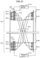
- FIG.33 is a detailed sectional view showing a configuration of an optical interconnection system according to a tenth embodiment of the present invention in which the units are connected by the optical beam propagated in a free-space.
- 33-1 denotes a unit(shelf); 33-2, a board; 33-3, a main signal VCSEL array; 33-4, a monitor beam VCSEL array; 33-5, a lens array; 33-6, an LC microprism array used as a deflection array device for optical interconnection; 33-7, a variable apex angle prism used as a beam array batch deflection control device; 33-8, a prism mirror; 33-9, an optical beam array; 33-10, a photodetector array; 33-11, an x-y position sensor; and 33-12, a feedback circuit which controls the variable apex angle prism to receive the optical beam always at the same position when the feedback circuit receives an output from the x-y position sensor 33-11.
- a pitch between the optical beam arrays 33-9 is set relatively rough such as 1mm to 2mm.
- the feedback circuit 33-12 always receives location information of the monitor beam detected by the x-y position sensor 33-11, and then controls the variable apex angle prism 33-7 such that the main optical beam signal always inputs into the desired photodetector array even if bowing of the board, location displacement of the board, and location displacement between the units are caused because of any disturbance.
- FIG.34 is a view showing a configuration of a variable apex angle prism.
- the variable apex angle prism has been developed for the purpose of correcting optically unintentional movement of the hands in taking a picture by a video camera, a binocular, etc.
- 34-1 denotes a glass plate; 34-2, a flexible bellows; 34-3, a rotating actuator; 34-4, an input beam; and 34-5, an output beam.
- Two sheets of the glass plate 34-1 are attached on both ends of the flexible bellows 34-2, and then a liquid which has the same refractive index as the glass plate 34-1 is filled in the space constituted by these materials.
- Two sheets of the glass plates 34-1 are constituted such that their directions are varied by two rotating actuators 34-3.
- an angle of the flexible bellows 34-2 can be varied linearly from -2.0° to +2.0° .
- the deflection direction tunable device such as the LC microprism array 33-6
- some devices have an insufficient maximum deflection angle.
- a hologram device As a representative of the fixed-angle deflection device, there can be thought about a hologram device.
- a computer hologram is very useful since its deflection direction can be set freely by the computer.
- the prism array has such an advantage that it can be fabricated by polymethylmethacrylate, etc. at low cost.
- FIG.35A a polymethylmethacrylate prism array as the fixed-angle deflection device and the LC microprism array as the tunable light deflection control array device is shown in combination in FIG.35A.
- 35-1 denotes the polymethylmethacrylate prism array.
- Respective prisms are arranged at a pitch of 1 mm in the polymethylmethacrylate prism array 35-1. Apex angles of respective prism are so designed that the light can be transmitted perfectly between a distance of 25cm by cross interconnection.
- FIG.35B is a view showing an example of the apex angles of respective.
- Main optical interconnection is established via the polymethylmethacrylate prism array 35-1 and the LC microprism array 33-6 is used to correction the optical interconnection.
- the position to which the incident optical beam 36-3 is irradiated can be expressed by a current output ratio. Accordingly, if the position of the monitor beam on the Si photodiode 36-4 is stored in the x-y position sensor 33-11 when the VCSEL array and the photodetector array are suitably optical-interconnected in an initial state and then the deflection control device is operated by feedback to restore the monitor beam to the initial position on the Si photodiode 36-4 when the optical interconnection is interrupted by virtue of disturbance, the VCSEL array in a certain unit and the photodetector array in another unit are always connected via the optical beam.
- the optical beams whose direction is finely adjusted by the LC microprism array 33-6 and is turned by the prism mirror 33-8 by about 90° are controlled to be input into the prism mirror 33-8 of the desired unit 33-1.
- the optical beams which are input into the desired unit 33-1 are turned by the prism mirror 33-8 by about 90° to input into the photodetector array 33-10 via the lens array 33-5.
- the LC microprism array has been used as the tunable light deflection control array device, but the micro mirror array, the LC deflection device, the rotation mirror array, and the rotation prism array may be used selectively. Still further, if the fixed-angle light deflection device is employed, the hologram device, and the prism array device may be used in addition to the above polymethylmethacrylate prism array. In addition, a combination of the fixed-angle deflection control device and the tunable light deflection control array device may be used.
- FIG.37 is a detailed sectional view showing a configuration of a unit-to-unit optical interconnection system according to an eleventh embodiment of the present invention.
- the optical interconnection can be established to form images of the light source on the photodetector array by the macro lens in the eleventh embodiment.
- 37-1 is a macro lens which forms the imaged transmitted from the main signal VCSEL array 33-3 on the photodetector array 33-10.
- Remaining configuration of the eleventh embodiment is similar to the tenth embodiment. Since an image forming system is employed in the eleventh embodiment, pitches of the main signal VCSEL array 33-3 and the photodetector array 33-10 are set relatively finely, e.g., several tens ⁇ m to several hundreds ⁇ m.
- the LC microprism array has been used as the tunable light deflection control array device, but the micro mirror array, the LC deflection device, the rotation mirror array, and the rotation prism array may be used selectively. Further, if the fixed-angle light deflection device is employed, the hologram device, and the prism array device may be used as well as the above polymethylmethacrylate prism array. In addition, a combination of the fixed-angle deflection control device and the tunable light deflection control array device may be used.
- FIG.38 is a detailed sectional view showing a configuration of a unit-to-unit optical interconnection system according to a twelfth embodiment of the present invention.
- the units are connected by turning the optical beam by the prism mirror by a substantially right angle in the tenth embodiment, the optical interconnection can be established between the main signal VCSEL array and the photodetector array by using paired polarization beam splitter and polarization control array device in the twelfth embodiment.
- 38-2 denotes a polarization beam splitter; 38-3, a twisted nematic LC; 38-4, an optical beam which proceeds upwardly; and 38-5, an optical beam which proceeds downward.
- Other configuration of the twelfth embodiment is similar to the first embodiment. In FIG.38, though only two stages are depicted, actually the unit-to-unit optical interconnection system of the twelfth embodiment is constructed in a multistage fashion and thus the optical interconnection can be established between the arbitrary units.
- the optical beams are then turned by the polarization beam splitter 38-2 in the target unit by 90° and thus the optical beam propagates the photodetector array 33-10 in the target unit.
- the optical beams are passed through the twisted nematic LC 38-3 in the non-target unit, its polarization direction is not varied.
- the optical beams propagates straight as they are through the polarization beam splitter 38-2 in the non-target unit.
- the target unit can be designated.
- the optical beams are turned by the polarization beam splitter 38-2 by 90 ° and then input into the photodetector array 33-10 via the lens array 33-5.
- An operation of a feedback circuit 33-12 is the same as the first embodiment.
- the LC microprism array has been used as the tunable light deflection control array device, but the micro mirror array, the LC deflection device, the rotation mirror array, and the rotation prism array may be used selectively. Further, if the fixed-angle light deflection device is employed, the hologram device, and the prism array device may be used as well as the above polymethylmethacrylate prism array. In addition, a combination of the fixed-angle deflection control device and the tunable light deflection control array device may be used.
- free-space optical interconnection system has been employed as the board-to-board interconnection between different units in the unit-to-unit optical interconnection system according to the present invention.
- three items can be listed as follows.
- an approach for establishing the free-space optical interconnection system between the boards in a certain unit and a different unit arbitrarily can be provided by introducing the light deflection control array device which is capable of controlling the propagation direction of the optical beam.
- the optical interconnection system can include a feedback control system which can restore the original optical interconnection even if the optical beam alignment is shifted by virtue of any external force.
- the optical interconnection system can be realized by inserting the macro lens between the units to thus form images of the transmitter array on the input side on the photodetector array on the output side. In this case, the units can be connected by the images instead of the optical beams. Also, in this case, the optical interconnection can always be maintained by providing the batch deflection control device.
Landscapes
- Physics & Mathematics (AREA)
- General Physics & Mathematics (AREA)
- Optics & Photonics (AREA)
- Optical Communication System (AREA)
- Mechanical Light Control Or Optical Switches (AREA)
- Liquid Crystal (AREA)
- Use Of Switch Circuits For Exchanges And Methods Of Control Of Multiplex Exchanges (AREA)
Applications Claiming Priority (9)
| Application Number | Priority Date | Filing Date | Title |
|---|---|---|---|
| JP14024396 | 1996-06-03 | ||
| JP14024396 | 1996-06-03 | ||
| JP140243/96 | 1996-06-03 | ||
| JP1564097 | 1997-01-29 | ||
| JP15640/97 | 1997-01-29 | ||
| JP1564097 | 1997-01-29 | ||
| JP64830/97 | 1997-03-18 | ||
| JP6483097 | 1997-03-18 | ||
| JP06483097A JP3427920B2 (ja) | 1996-06-03 | 1997-03-18 | ボード間光インタコネクション装置 |
Publications (3)
| Publication Number | Publication Date |
|---|---|
| EP0811862A2 true EP0811862A2 (fr) | 1997-12-10 |
| EP0811862A3 EP0811862A3 (fr) | 2001-12-19 |
| EP0811862B1 EP0811862B1 (fr) | 2004-08-25 |
Family
ID=27281095
Family Applications (1)
| Application Number | Title | Priority Date | Filing Date |
|---|---|---|---|
| EP97108914A Expired - Lifetime EP0811862B1 (fr) | 1996-06-03 | 1997-06-03 | Système d'interconnection optique carte-à-carte et unité-à-unité |
Country Status (3)
| Country | Link |
|---|---|
| US (1) | US5920664A (fr) |
| EP (1) | EP0811862B1 (fr) |
| DE (1) | DE69730378T2 (fr) |
Cited By (14)
| Publication number | Priority date | Publication date | Assignee | Title |
|---|---|---|---|---|
| WO2001026255A1 (fr) * | 1999-10-01 | 2001-04-12 | Eci Telecom Ltd. | Procede et dispositif d'alignement d'interconnexions optiques entre plaquettes de circuit imprime |
| EP1284429A1 (fr) * | 2001-08-17 | 2003-02-19 | Lucent Technologies Inc. | Systeme d'interconnexion de processeurs |
| EP1284430A1 (fr) * | 2001-08-17 | 2003-02-19 | Lucent Technologies Inc. | Méthode et appareil pour l'interconnexion de processeurs par WDM |
| EP1291693A1 (fr) * | 2001-08-17 | 2003-03-12 | Lucent Technologies Inc. | Installation d'unités de traitement qui sont connectées entre-elles par optique de volume |
| WO2004006617A1 (fr) * | 2002-07-04 | 2004-01-15 | Cambridge University Technical Services Limited | Paquet electro-optique hybride et commutateur de cellule |
| US7162158B2 (en) | 2001-08-17 | 2007-01-09 | Lucent Technologies Inc. | Interconnecting processing units of a stored program controlled system using space division multiplexed free space optics |
| US7229218B2 (en) | 2004-09-20 | 2007-06-12 | Hewlett-Packard Development Company, L.P. | Apparatus and method of providing an optical connection between PC boards for optical communication |
| US7251388B2 (en) | 2004-08-10 | 2007-07-31 | Hewlett-Packard Development Company, L.P. | Apparatus for providing optical communication between integrated circuits of different PC boards and an integrated circuit assembly for use therein |
| US7269321B2 (en) | 2004-08-10 | 2007-09-11 | Hewlett-Packard Development Company, L.P. | System and method of configuring fiber optic communication channels between arrays of emitters and detectors |
| US7623783B2 (en) | 2004-08-10 | 2009-11-24 | Hewlett-Packard Development Company, L.P. | System and method of self-configuring optical communication channels between arrays of emitters and detectors |
| US7623793B2 (en) | 2004-08-10 | 2009-11-24 | Hewlett-Packard Development Company, L.P. | System and method of configuring fiber optic communication channels between arrays of emitters and detectors |
| US7653108B2 (en) | 2004-09-09 | 2010-01-26 | Hewlett-Packard Development Company, L.P. | Apparatus and method of establishing optical communication channels between a steerable array of laser emitters and an array of optical detectors |
| US7809278B2 (en) | 2004-07-26 | 2010-10-05 | Hewlett-Packard Development Company, L.P. | Apparatus and method of providing separate control and data channels between arrays of light emitters and detectors for optical communication and alignment |
| CN113917761A (zh) * | 2021-09-23 | 2022-01-11 | 之江实验室 | 一种基于角度无惯性反馈校正的光束稳定装置 |
Families Citing this family (27)
| Publication number | Priority date | Publication date | Assignee | Title |
|---|---|---|---|---|
| JPH1184409A (ja) * | 1997-09-01 | 1999-03-26 | Canon Inc | 静止画像表示装置 |
| US6377599B1 (en) * | 1999-01-12 | 2002-04-23 | Iridex Corporation | Focusability enhancing optic for a laser diode |
| US6396976B1 (en) * | 1999-04-15 | 2002-05-28 | Solus Micro Technologies, Inc. | 2D optical switch |
| US6829237B2 (en) | 2000-10-06 | 2004-12-07 | Irvine Sensors Corporation | High speed multi-stage switching network formed from stacked switching layers |
| US6823100B1 (en) * | 2001-08-27 | 2004-11-23 | Incucomm, Inc. | Optical backplane for use with a communications equipment chassis and method of operation therefor |
| US6970649B2 (en) * | 2001-10-30 | 2005-11-29 | International Business Machines Corporation | WDMA free space broadcast technique for optical backplanes and interplanar communications |
| US6819815B1 (en) * | 2001-12-12 | 2004-11-16 | Calient Networks | Method and apparatus for indirect adjustment of optical switch reflectors |
| JP3703433B2 (ja) * | 2002-01-08 | 2005-10-05 | キヤノン株式会社 | 光走査装置及び画像形成装置 |
| US7978981B2 (en) * | 2002-02-22 | 2011-07-12 | Avago Technologies Fiber Ip (Singapore) Pte. Ltd. | Structure and apparatus for a very short haul, free space, and fiber optic interconnect and data link |
| DE60301637T2 (de) * | 2002-04-16 | 2006-06-22 | Robert Bosch Gmbh | Verfahren zur Datenübertragung in einem Kommunikationssystem |
| DE10229428A1 (de) * | 2002-07-01 | 2004-01-15 | Sick Ag | Detektoreinheit |
| US7336900B2 (en) * | 2003-10-30 | 2008-02-26 | International Business Machines Corporation | Byte-wide optical backplane switch |
| JP4555631B2 (ja) * | 2004-08-27 | 2010-10-06 | 富士通株式会社 | 光伝送回路装置 |
| US20060093361A1 (en) * | 2004-11-03 | 2006-05-04 | Fenwick David M | Optical bus system |
| US7416352B2 (en) * | 2005-09-08 | 2008-08-26 | Northrop Grumman Corporation | Optical multi-channel free space interconnect |
| JP4384127B2 (ja) * | 2006-03-22 | 2009-12-16 | トヨタ自動車株式会社 | 複数枚の回路基板が所定距離を隔てて積層されているモジュールと、そのモジュール用の光コネクタ |
| US8244134B2 (en) | 2007-06-19 | 2012-08-14 | Charles Santori | Optical interconnect |
| US8929741B2 (en) | 2007-07-30 | 2015-01-06 | Hewlett-Packard Development Company, L.P. | Optical interconnect |
| KR101395169B1 (ko) * | 2008-01-31 | 2014-05-16 | 휴렛-팩커드 디벨롭먼트 컴퍼니, 엘.피. | 자유 공간 광인터커넥트 |
| US8510244B2 (en) | 2009-03-20 | 2013-08-13 | ISC8 Inc. | Apparatus comprising artificial neuronal assembly |
| US9709829B2 (en) * | 2011-11-18 | 2017-07-18 | Vuzix Corporation | Beam steering device |
| EP2881773B1 (fr) * | 2013-12-03 | 2018-07-11 | ams AG | Dispositif semi-conducteur avec miroir intégré et procédé de production d'un dispositif semi-conducteur avec miroir intégré |
| EP2985636B1 (fr) * | 2014-08-11 | 2018-07-25 | Leuze electronic GmbH + Co KG | Procédé d'alignement d'un dispositif de capteurs |
| JP6412779B2 (ja) * | 2014-11-20 | 2018-10-24 | 株式会社フジクラ | 光ファイバテープ心線、光ファイバケーブル、および、光ファイバテープ心線の製造方法 |
| WO2018102135A1 (fr) * | 2016-11-29 | 2018-06-07 | Corning Optical Communications LLC | Ruban flexible fritté au laser |
| CN109844597B (zh) * | 2016-12-20 | 2020-11-20 | 古河电气工业株式会社 | 光纤间歇带芯线的制造方法和光纤间歇带芯线 |
| US12395242B2 (en) | 2023-06-15 | 2025-08-19 | Microsoft Technology Licensing, Llc | Optical transport terminal node architecture with free space optical backplane |
Family Cites Families (4)
| Publication number | Priority date | Publication date | Assignee | Title |
|---|---|---|---|---|
| US5500523A (en) * | 1990-09-21 | 1996-03-19 | Nippon Sheet Glass Co. Ltd. | Optical information transmitting device and method of manufacturing same |
| GB9024713D0 (en) * | 1990-11-14 | 1991-01-02 | Plessey Telecomm | Optical backplane interconnecting circuit boards |
| US5170269A (en) * | 1991-05-31 | 1992-12-08 | Texas Instruments Incorporated | Programmable optical interconnect system |
| DE4434358C1 (de) * | 1994-09-26 | 1996-03-28 | Siemens Ag | Optische Datenverbindung zwischen benachbarten Baugruppen |
-
1997
- 1997-06-03 EP EP97108914A patent/EP0811862B1/fr not_active Expired - Lifetime
- 1997-06-03 DE DE69730378T patent/DE69730378T2/de not_active Expired - Fee Related
- 1997-06-03 US US08/868,177 patent/US5920664A/en not_active Expired - Fee Related
Cited By (19)
| Publication number | Priority date | Publication date | Assignee | Title |
|---|---|---|---|---|
| US6583904B1 (en) | 1999-10-01 | 2003-06-24 | Eci Telecom Ltd. | Method and apparatus for aligning optical interconnections between printed circuit boards |
| WO2001026255A1 (fr) * | 1999-10-01 | 2001-04-12 | Eci Telecom Ltd. | Procede et dispositif d'alignement d'interconnexions optiques entre plaquettes de circuit imprime |
| US7162158B2 (en) | 2001-08-17 | 2007-01-09 | Lucent Technologies Inc. | Interconnecting processing units of a stored program controlled system using space division multiplexed free space optics |
| EP1291693A1 (fr) * | 2001-08-17 | 2003-03-12 | Lucent Technologies Inc. | Installation d'unités de traitement qui sont connectées entre-elles par optique de volume |
| EP1284430A1 (fr) * | 2001-08-17 | 2003-02-19 | Lucent Technologies Inc. | Méthode et appareil pour l'interconnexion de processeurs par WDM |
| US6993260B2 (en) | 2001-08-17 | 2006-01-31 | Lucent Technologies Inc. | Interconnecting processing units of a stored program controlled system using free space optics |
| US7110679B2 (en) | 2001-08-17 | 2006-09-19 | Lucent Technologies Inc. | Installation of processing units into a stored program controlled system wherein the component processing units are interconnected via free space optics |
| EP1284429A1 (fr) * | 2001-08-17 | 2003-02-19 | Lucent Technologies Inc. | Systeme d'interconnexion de processeurs |
| WO2004006617A1 (fr) * | 2002-07-04 | 2004-01-15 | Cambridge University Technical Services Limited | Paquet electro-optique hybride et commutateur de cellule |
| US7809278B2 (en) | 2004-07-26 | 2010-10-05 | Hewlett-Packard Development Company, L.P. | Apparatus and method of providing separate control and data channels between arrays of light emitters and detectors for optical communication and alignment |
| US7251388B2 (en) | 2004-08-10 | 2007-07-31 | Hewlett-Packard Development Company, L.P. | Apparatus for providing optical communication between integrated circuits of different PC boards and an integrated circuit assembly for use therein |
| US7269321B2 (en) | 2004-08-10 | 2007-09-11 | Hewlett-Packard Development Company, L.P. | System and method of configuring fiber optic communication channels between arrays of emitters and detectors |
| US7623783B2 (en) | 2004-08-10 | 2009-11-24 | Hewlett-Packard Development Company, L.P. | System and method of self-configuring optical communication channels between arrays of emitters and detectors |
| US7623793B2 (en) | 2004-08-10 | 2009-11-24 | Hewlett-Packard Development Company, L.P. | System and method of configuring fiber optic communication channels between arrays of emitters and detectors |
| US7653108B2 (en) | 2004-09-09 | 2010-01-26 | Hewlett-Packard Development Company, L.P. | Apparatus and method of establishing optical communication channels between a steerable array of laser emitters and an array of optical detectors |
| US9142938B2 (en) | 2004-09-09 | 2015-09-22 | Hewlett-Packard Development Company, L.P. | Apparatus and method of establishing optical communication channels between a steerable array of laser emitters and an array of optical detectors |
| US7229218B2 (en) | 2004-09-20 | 2007-06-12 | Hewlett-Packard Development Company, L.P. | Apparatus and method of providing an optical connection between PC boards for optical communication |
| CN113917761A (zh) * | 2021-09-23 | 2022-01-11 | 之江实验室 | 一种基于角度无惯性反馈校正的光束稳定装置 |
| CN113917761B (zh) * | 2021-09-23 | 2024-01-02 | 之江实验室 | 一种基于角度无惯性反馈校正的光束稳定装置 |
Also Published As
| Publication number | Publication date |
|---|---|
| EP0811862B1 (fr) | 2004-08-25 |
| DE69730378T2 (de) | 2005-08-18 |
| DE69730378D1 (de) | 2004-09-30 |
| US5920664A (en) | 1999-07-06 |
| EP0811862A3 (fr) | 2001-12-19 |
Similar Documents
| Publication | Publication Date | Title |
|---|---|---|
| EP0811862B1 (fr) | Système d'interconnection optique carte-à-carte et unité-à-unité | |
| US5648859A (en) | Liquid crystal microprism array, free-space optical interconnector, and optical switch | |
| EP0477036B1 (fr) | Dispositif pour la transmission d'informations optiques | |
| US5500523A (en) | Optical information transmitting device and method of manufacturing same | |
| US6775480B1 (en) | Free space optical interconnect system | |
| Crossland et al. | Holographic optical switching: the" ROSES" demonstrator | |
| US5162944A (en) | Optical space switch and network for such optical space switches | |
| US8885991B2 (en) | Circuit switched optical interconnection fabric | |
| CA1298116C (fr) | Commutateur spatial optique bidirectionnel | |
| JP2000509509A (ja) | 完全に光学的なスイッチ | |
| US6839472B1 (en) | Solid state optical interconnect system | |
| US6711315B1 (en) | 3-D electro optical switch | |
| JP7679522B2 (ja) | 拡張可能な光回路スイッチ構造 | |
| JPH1131035A (ja) | 光バスおよび信号処理装置 | |
| JP4368074B2 (ja) | 光スイッチ装置 | |
| US6317532B1 (en) | Method and apparatus for low loss via geometrical optimization in free-space micro-machined optical switches | |
| US6172783B1 (en) | Optical bus and signal processor | |
| JP3427920B2 (ja) | ボード間光インタコネクション装置 | |
| US20050018954A1 (en) | Liquid crystal optical switch with bumt-in control | |
| WO2000016503A1 (fr) | Systeme d'interconnexion optique sans contrainte d'espace | |
| Hirabayashi et al. | Optical backplane with free-space optical interconnections using tunable beam deflectors and a mirror for bookshelf-assembled terabit per second class asynchronous transfer mode switch | |
| WO2001090823A1 (fr) | Composant electro-optique possedant un etat de phase reconfigurable | |
| White et al. | An optically connected parallel machine: Design, performance and application | |
| JPH10274791A (ja) | ボード間及びユニット間の光インタコネクション装置 | |
| Kim et al. | A method for rebroadcasting signals in an optical backplane bus system |
Legal Events
| Date | Code | Title | Description |
|---|---|---|---|
| PUAI | Public reference made under article 153(3) epc to a published international application that has entered the european phase |
Free format text: ORIGINAL CODE: 0009012 |
|
| 17P | Request for examination filed |
Effective date: 19970701 |
|
| AK | Designated contracting states |
Kind code of ref document: A2 Designated state(s): AT BE CH DE DK ES FI FR GB GR IE IT LI LU MC NL PT SE Kind code of ref document: A2 Designated state(s): DE FR GB |
|
| RIC1 | Information provided on ipc code assigned before grant |
Free format text: 7G 02B 6/43 A |
|
| PUAL | Search report despatched |
Free format text: ORIGINAL CODE: 0009013 |
|
| AK | Designated contracting states |
Kind code of ref document: A3 Designated state(s): AT BE CH DE DK ES FI FR GB GR IE IT LI LU MC NL PT SE |
|
| AKX | Designation fees paid |
Free format text: DE FR GB |
|
| 17Q | First examination report despatched |
Effective date: 20020912 |
|
| GRAP | Despatch of communication of intention to grant a patent |
Free format text: ORIGINAL CODE: EPIDOSNIGR1 |
|
| GRAS | Grant fee paid |
Free format text: ORIGINAL CODE: EPIDOSNIGR3 |
|
| GRAA | (expected) grant |
Free format text: ORIGINAL CODE: 0009210 |
|
| AK | Designated contracting states |
Kind code of ref document: B1 Designated state(s): DE FR GB |
|
| REG | Reference to a national code |
Ref country code: GB Ref legal event code: FG4D |
|
| REG | Reference to a national code |
Ref country code: IE Ref legal event code: FG4D |
|
| REF | Corresponds to: |
Ref document number: 69730378 Country of ref document: DE Date of ref document: 20040930 Kind code of ref document: P |
|
| ET | Fr: translation filed | ||
| PLBE | No opposition filed within time limit |
Free format text: ORIGINAL CODE: 0009261 |
|
| STAA | Information on the status of an ep patent application or granted ep patent |
Free format text: STATUS: NO OPPOSITION FILED WITHIN TIME LIMIT |
|
| 26N | No opposition filed |
Effective date: 20050526 |
|
| PGFP | Annual fee paid to national office [announced via postgrant information from national office to epo] |
Ref country code: DE Payment date: 20070626 Year of fee payment: 11 |
|
| PGFP | Annual fee paid to national office [announced via postgrant information from national office to epo] |
Ref country code: GB Payment date: 20070604 Year of fee payment: 11 |
|
| PGFP | Annual fee paid to national office [announced via postgrant information from national office to epo] |
Ref country code: FR Payment date: 20070621 Year of fee payment: 11 |
|
| GBPC | Gb: european patent ceased through non-payment of renewal fee |
Effective date: 20080603 |
|
| REG | Reference to a national code |
Ref country code: FR Ref legal event code: ST Effective date: 20090228 |
|
| PG25 | Lapsed in a contracting state [announced via postgrant information from national office to epo] |
Ref country code: DE Free format text: LAPSE BECAUSE OF NON-PAYMENT OF DUE FEES Effective date: 20090101 |
|
| PG25 | Lapsed in a contracting state [announced via postgrant information from national office to epo] |
Ref country code: GB Free format text: LAPSE BECAUSE OF NON-PAYMENT OF DUE FEES Effective date: 20080603 |
|
| PG25 | Lapsed in a contracting state [announced via postgrant information from national office to epo] |
Ref country code: FR Free format text: LAPSE BECAUSE OF NON-PAYMENT OF DUE FEES Effective date: 20080630 |