EP0811986B1 - Seitenmodusspeicher mit Mehrpegelspeicherzellen - Google Patents
Seitenmodusspeicher mit Mehrpegelspeicherzellen Download PDFInfo
- Publication number
- EP0811986B1 EP0811986B1 EP96830318A EP96830318A EP0811986B1 EP 0811986 B1 EP0811986 B1 EP 0811986B1 EP 96830318 A EP96830318 A EP 96830318A EP 96830318 A EP96830318 A EP 96830318A EP 0811986 B1 EP0811986 B1 EP 0811986B1
- Authority
- EP
- European Patent Office
- Prior art keywords
- memory
- current
- page
- mw2m
- memory device
- Prior art date
- Legal status (The legal status is an assumption and is not a legal conclusion. Google has not performed a legal analysis and makes no representation as to the accuracy of the status listed.)
- Expired - Lifetime
Links
Images


Classifications
-
- G—PHYSICS
- G11—INFORMATION STORAGE
- G11C—STATIC STORES
- G11C11/00—Digital stores characterised by the use of particular electric or magnetic storage elements; Storage elements therefor
- G11C11/56—Digital stores characterised by the use of particular electric or magnetic storage elements; Storage elements therefor using storage elements with more than two stable states represented by steps, e.g. of voltage, current, phase, frequency
- G11C11/5621—Digital stores characterised by the use of particular electric or magnetic storage elements; Storage elements therefor using storage elements with more than two stable states represented by steps, e.g. of voltage, current, phase, frequency using charge storage in a floating gate
-
- G—PHYSICS
- G11—INFORMATION STORAGE
- G11C—STATIC STORES
- G11C11/00—Digital stores characterised by the use of particular electric or magnetic storage elements; Storage elements therefor
- G11C11/56—Digital stores characterised by the use of particular electric or magnetic storage elements; Storage elements therefor using storage elements with more than two stable states represented by steps, e.g. of voltage, current, phase, frequency
- G11C11/5621—Digital stores characterised by the use of particular electric or magnetic storage elements; Storage elements therefor using storage elements with more than two stable states represented by steps, e.g. of voltage, current, phase, frequency using charge storage in a floating gate
- G11C11/5642—Sensing or reading circuits; Data output circuits
-
- G—PHYSICS
- G11—INFORMATION STORAGE
- G11C—STATIC STORES
- G11C2211/00—Indexing scheme relating to digital stores characterized by the use of particular electric or magnetic storage elements; Storage elements therefor
- G11C2211/56—Indexing scheme relating to G11C11/56 and sub-groups for features not covered by these groups
- G11C2211/563—Multilevel memory reading aspects
- G11C2211/5632—Multilevel reading using successive approximation
-
- G—PHYSICS
- G11—INFORMATION STORAGE
- G11C—STATIC STORES
- G11C2211/00—Indexing scheme relating to digital stores characterized by the use of particular electric or magnetic storage elements; Storage elements therefor
- G11C2211/56—Indexing scheme relating to G11C11/56 and sub-groups for features not covered by these groups
- G11C2211/563—Multilevel memory reading aspects
- G11C2211/5634—Reference cells
Definitions
- the present invention relates to a page-mode memory device with multiple-level memory cells.
- FIG. 1 schematically shows the structure of a conventional page-mode memory device: memory cells MC, for example EPROM or Flash EPROM memory cells, are arranged in rows R and columns C of a memory matrix 1. Each memory cell is for example a floating gate MOS transistor having a drain electrode connected to a respective column C, a source electrode connected to ground and a control gate electrode connected to a respective row R.
- memory cells MC for example EPROM or Flash EPROM memory cells
- Each memory cell is for example a floating gate MOS transistor having a drain electrode connected to a respective column C, a source electrode connected to ground and a control gate electrode connected to a respective row R.
- a line decoder circuit 2 is supplied with line address signals LADD for decoding a configuration of the line address signals and for accordingly selecting one of the rows R of memory cells of the memory matrix 1.
- a plurality of sensing circuits 3 is also provided, each one associated to a respective column C of the memory matrix 1.
- the number of sensing circuits 3 to be provided is strictly equal to the number of memory words per memory page, multiplied by the word size: in the above-mentioned example, 256 sensing circuits 3 are to be provided.
- a plurality of memory registers MR1-MRm is also provided for storing all the memory words MW1-MWm of a selected memory page MP1-MPn.
- Each memory register MR1-MRm has the same size as the size of the memory words (in the previous example, each memory register must be capable of storing sixteen bits).
- the plurality of memory registers MR1-MRm forms a so-called "line buffer".
- a word decoder circuit 5 supplied with word address signals WADD, allows to select one memory word among the plurality of memory words MW1-MWm of the selected memory page MP1-MPn, and to supply the selected memory word to output buffer circuits 6 of the memory device.
- a read operation of a page-mode memory device starts when one or more of the line address signals LADD change: the line decoder circuit 2 decodes the current configuration of the line address signals LADD and accordingly to the new configuration selects one of the rows R of memory cells of the memory matrix 1.
- the sensing circuits 3 read the content of the memory cells MC belonging to the selected row R, and the read data are stored in the memory registers MR1-MRm: in this way, all the memory words of the selected memory page are simultaneously read and the read data are stored in the line buffer, the information content of the selected memory page being loaded in the memory registers MR1-MRm of the line buffer.
- the word decoder circuit 5 selects, according to the configuration of the word address signals WADD, one of the plurality of memory words of the selected memory page and transfers the content of the selected memory word to the output buffer circuits 6.
- This kind of memory devices are particularly suitable in high-speed applications requiring low read times. However, they occupy a significant chip area, due to the great number of sensing circuits which must be provided (as already mentioned, in word page-mode memory device having a word size of sixteen bits, 256 sensing circuits must be provided instead of the 16 required in a non-paged memory device with the same word size). As already mentioned, the number of sensing circuits is directly dependent on the word size, and on the number of memory words per memory page. Also, this kind of memory devices shows a significant power consumption, because all the sensing circuits operate simultanoeusly.
- Serial-dichotomic sensing circuits for sensing, according to a serial-dichotomic method, multiple-level memory cells (i.e., memory cells which can be programmed in a plurality of programming states and which store more than one bit of information) are disclosed in the co-pending European Patent applications No. 95830023.8 and No. 95830110.3, both in the name of the same Applicant. These circuits occupy an area substantially equal to that of conventional sensing circuits for reading two-level memory cells, and have a similar power consumption.
- the present invention it is possible to increase the number of memory words per memory page without increasing the number of sensing circuits. This allows to increase the memory capacity without significantly increasing the chip area and the power consumption of the memory device.
- Fig. 1 schematically shows a conventional page-mode memory device, and has already been described.
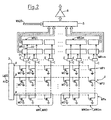
- Fig. 2 schematically shows the main circuit blocks of a page-mode memory device according to a first embodiment of the present invention.
- a memory matrix 1 of memory cells MC' is provided, the memory cells MC' being arranged in rows R and columns C.
- the memory cells MC' are for example floating-gate MOS transistors of the type conventionally used in EPROM or Flash EEPROMs devices.
- a line decoder 2 is supplied by Line address signals LADD which allow to select one row R of the memory matrix at a time. Each row R forms a memory page MP1-MPn of the memory device.
- each column C of the memory matrix 1 there is associated a respective sensing circuit 3' for reading the information content of the memory cell MC' belonging to the selected row R.
- each memory cell MC' is a four-levels memory cell, i.e. a memory cell capable of assuming four different programming states; a four-level memory cell, differently from conventional two-levels memory cells, is capable of storing two bits of information, instead of a single information bit.
- a four-level memory cell differently from conventional two-levels memory cells, is capable of storing two bits of information, instead of a single information bit.
- this is not to be intended as a limitation of the invention, the latter providing more generally for the use of multiple-level memory cells capable of storing b bits of information.
- the sensing circuits 3' differently from conventional sensing circuits used to read two-levels memory cells, must be capable of discriminating the four different programming states of the memory cells.
- Each sensing circuit 3' has two respective output signals 01 and 02, corresponding to the two bits of information that are stored in the memory cell MC' which is to be read.
- a first one 01 of the two output signals of a given sensing circuit 3' supply a respective memory unit of a memory register MR11-MR1m, and the other output signal 02 of the sensing circuit 3' supplies a respective memory unit of another memory register MR21-MR2m.
- Each memory register MR11-MR1m and MR21-MR2m has a size equal to the size of the memory words of the memory device.
- a word decoder 5, supplied with word address signals WADD, allows to select one memory word of the memory page, and to supply the selected word to output buffer circuits 6.
- the number of memory words MW1-MW2m per memory page MP1-MPn is double with respect to a conventional page-mode memory device having the same number of memory cells and the same number of sensing circuits, with a significant reduction of chip area and power consumption.
- This is made possible by the use of four-levels memory cells instead of conventional two-levels memory cells, and using sensing circuits 3' capable of discriminating the four different programming states of the four-level memory cells.
- the sensing circuits 3' are of the type described in the co-pending European Patent Application No. 95830023.8 or in the co-pending European Patent Application No. 95830110.3, both in the name of the same Applicant, the content of which is enclosed herein by reference.
- the sensing circuits 3' operate according to a serial-dichotomic sensing method which is also described in the first one of the two above-mentioned patent applications.
- the cell current is compared with a first reference current having a value comprised between a minimum and a maximum value of said set of cell current values, thus dividing said set of cell current values in two sub-sets to determine to which of the two sub-sets of cell current values the cell current belongs.
- the cell current is compared with a second reference current having a value comprised between a minimum and a maximum value of said sub-set, thus dividing the sub-set of cell current values in two further sub-sets to determine to which of said further sub-sets the cell current belongs, and so on until in the last step only two memory cell currents are left.
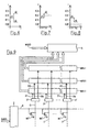
- Fig. 3 schematically shows the structure of the sensing circuits 3'.
- the circuit substantially comprises a digitally-driven variable reference current generator G for generating a variable reference current IR, a current comparator 7 for comparing the reference current IR generated by the variable reference current generator G with a current IC sunk by a memory cell MC' to be read (which is biased by a control gate voltage VG) and a successive approximation register 8 supplied by an output CMP of comparator 7.
- the successive approximation register 8 is further supplied by a preset signal PR and a timing signal CK, and generates the two output signals 01, 02 of the sensing circuit and digital control signals Q0, Q1 for the variable reference current generator G.
- Fig. 4 schematically shows the structure of the variable reference current generator G, which comprises three distinct reference current generators IR0, IR1 and Ioff.
- Ioff is an offset current generator which generates a constant current and is permanently connected to the non-inverting input of the current comparator 7.
- IR0 and IR1 can instead be selectively connected to the non-inverting input of current comparator 7 by means of respective switches SW0, SW1 respectively activated by the control signals Q0 and Q1.
- Fig. 5 is a circuit diagram of the successive approximation register 8.
- the circuit comprises two delay-type flip-flops FF0, FF1, each one having a clock input CK and a preset input PR.
- the clock inputs CK and the preset inputs PR of flip-flops FF0, FF1 are commonly connected to the timing signal CK and to the preset signal PR (more precisely, FF0 receives the logic complement of PR, as indicated by the Logic inversion dot at the input PR of FF0).
- Each flip-flop FF0, FF1 has a data input D0, D1, a "true” data output Q0, Q1 and a "logic complemented" data output Q0N, Q1N which is the logic complement of Q0, Q1, respectively.
- the true data output after a clock pulse takes the Logic value of the data input during said clock pulse.
- the data input D0 of flip-flop FF0 is supplied with the complemented data output Q0N of FF0 itself.
- the data input D1 of flip-flop FF1 is supplied with an output of a NOR gate 9 whose inputs are the output signal CMP of the current comparator 7 and and the complemented data output Q0N of flip-flop FF0.
- the output signal CMP of the current comparator 7, once complemented, is the output signal 01 of the sensing circuit 3', and forms the least significant bit of a two-bit code stored in the memory cell MC' to be sensed;
- the true data output Q1 of flip-flop FF1 is the output signal 02 of the sensing circuit 3' and forms the most significant bit of said two-bit code.
- the true data outputs Q0, Q1 of flip-flops FF0, FF1 are the control signals for the switches SW0, SW1 of the variable reference current generator G; switch SW0,SW1 closes when the respective control signal Q0, Q1 is a logic "1", otherwise switch SW0, SW1 is open.
- Fig. 6 is a diagram showing, in the ordinate axis, the distribution of current values IC for a four-levels memory cell to be sensed.
- the four different programming states correspond to four different values IC0-IC3 of the current IC sunk by the memory cell.
- Fig. 6 also shows, on branches of a decision tree, the three different values I0-I2 that can be taken by the reference current IR; it is to be noted that the reference current values I0-I2 are intermediate between successive values of the memory cell current IC.
- I0 is equal to Ioff
- I1 is equal to Ioff+IR0
- I2 is equal to Ioff+IR1.
- the most significant bit 02 of the two-bit code stored in the memory cell to be read is available after the first step of the sensing process, while the least significant bit 01 of said two-bit code is available after (3/2)T from the beginning of the sensing process, where T is the period of the timing signal CK, i.e. before the end of the second step of the sensing process.
- T is the period of the timing signal CK, i.e. before the end of the second step of the sensing process.
- the successive approximation register 8 automatically presets in the correct initial condition.
- the time needed for reading the content of the 2m memory words of a memory page is higher than that necessary to read m memory words in a conventional page-mode memory device with two-level memory cells.
- twice the number of memory words are now stored in the line buffer, so that the higher time needed to load the content of a memory page in the line buffer is compensated by the fact that there is a greater probability that a subsequent access to the memory device "hits" a memory word belonging to the same memory page.
- the higher time necessary to load a memory page in the line buffer is thus compensated by a higher probability of high-speed accesses to the line buffer.
- the sensing circuits 3' must be able of discriminating the c distinct programming states of the memory cells, and have b output signals 01-0b.
- Output signal 01 supplies a respective memory unit of a first memory register MR11
- output signal 02 supplies a respective memory unit of a memory register MR21
- output signal 0b supplying a respective memory unit of a memory register MRb1.
- the number of memory words per memory page is b times the number of memory words of a conventional page-mode memory device having the same number of memory cells and the same number of sensing circuits, with a great increase in the memory capacity without a corresponding increase of the chip area and of the power consumption.
- the sensing circuits can be advantageously of the kind suitable to implement the serial-dichotomic sensing method.
- the structure of the sensing circuits 3' can be easily derived by generalization from the structure shown in Figs. 3 to 5.
- the number of bits per memory cell is not necessarily a power of 2 (2,4,8,16... bits per memory cell), but can be any integer number.
- the line buffer (memory registers MR11-MR1m, MR21-MR2m) and the memory word selection circuit 5 could be eliminated, provided that the possibility of a random access to the memory words of a memory page is abandoned for a sequential reading of the memory words of the memory page.
- a parallel input-serial output (PISO) memory register for generating a serial stream of bits.
- the PISO registers are loaded with new memory words of the selected memory page.
Landscapes
- Engineering & Computer Science (AREA)
- Computer Hardware Design (AREA)
- Read Only Memory (AREA)
Claims (10)
- Seitenmode-Halbleitervorrichtung mit einer Matrix (1) aus Speicherzellen (MC'), die in Zeilen (R) und Spalten (C) angeordnet sind, wobei jede Zeile (R) eine Speicherseite (MP1-MPn) der Speichervorrichtung bildet und wenigstens eine Gruppe (MW1, MW2-MW2m-1, MW2m) von Speicherzellen (MC') aufweist, einer Speicherseiten-Auswahleinrichtung (2) zum Auswählen einer Zeile (R) der Matrix (1) und einer Vielzahl von Leseschaltungen (3'), von welchen jede einer jeweiligen Spalte (C) der Matrix zugeordnet ist, dadurch gekennzeichnet, dass die Speicherzellen (MC') Mehrpegel-Spelcherzellen sind, die in einer Vielzahl von c=2b, wobei b > 1 gilt, Programmierzuständen programmiert werden können, um b Informationsbits zu speichern, und dass die Leseschaltungen (3') seriellbinäre Leseschaltungen sind, die in einer Anzahl b von aufeinander folgenden Approximationsschritten die in den Speicherzellen (MC') gespeicherten b Informationsbits bestimmen können, wobei bei jedem Schritt eines der b Informationsbits bestimmt wird, wobei die wenigstens eine Gruppe (MW1, MW2-MW2m-1, MW2m) von Speicherzellen (MC') einer Zeile (R) eine Anzahl b von Speicherworten einer Speicherseite (MP1-MPn) bildet.
- Speichervorrichtung nach Anspruch 1, dadurch gekennzeichnet, dass jede Zeile (R) eine Vielzahl der Gruppen (MW1, MW2-MW2m-1, MW2m) von Speicherzellen (MC') aufweist, wobei jede Gruppe eine Anzahl b von Speicherworten bildet.
- Speichervorrichtung nach Anspruch 2, dadurch gekennzeichnet, dass sie eine Vielzahl von Speicherregistem (MR11-MR1m, MR21-MR2m; MR11-MR1b) gleich der Anzahl von Speicherworten (MW1, MW2-MW2m-1, MW2m) aufweist, die in jeder Speicherseite (MP1-MPn) enthalten sind, wobei die Vielzahl von Speicherregistern in Gruppen von b Speicherregistem aufgeteilt ist, die jeweiligen Gruppen von b Leseschaltungen (3') zugeordnet sind, wobei jede Leseschaltung (3') eine Anzahl b von Ausgangssignalen (O1, O2; O1-Ob) hat, von welchen jedes eine jeweilige Speichereinheit eines jeweiligen Speicherregisters der zugeordneten Gruppe von Speicherregistern versorgt, wobei jede Gruppe von Speicherregistern durch die in einer jeweiligen Gruppe (MW1, MW2-MW2m-1, MW2m) von Speicherzellen (MC') einer ausgewählten Zeile (R) gespeicherten b Speicherworte geladen wird.
- Speichervorrichtung nach Anspruch 3, dadurch gekennzeichnet, dass sie eine Speicherwort-Auswahleinrichtung (5) zum Auswählen eines unter der Vielzahl von Speicherregistem (MR11-MR1m, MR21-MR2m; MR11-MR1b) aufweist.
- Speichervorrichtung nach Anspruch 1, dadurch gekennzeichnet, dass ein Paralleleingabe/Seriellausgabe-Speicherregister der wenigstens einen Gruppe (MW1, MW2-MW2m-1, MW2m) zugeordnet ist, um bei jedem Approximationsschritt eines der b Speicherworte der Speicherseite zu speichern und um die Bits des Speicherworts seriell auszugeben.
- Speichervorrichtung nach Anspruch 1, dadurch gekennzeichnet, dass jede Leseschaltung (3') einen variablen Referenzstromgenerator (G) aufweist, der einen Referenzstrom (IR) erzeugt, der Werte (I0-I2) annehmen kann, die zwischen einer Vielzahl von Werten (IC0-IC3) eines Speicherzellenstroms (IC) sind, für den eine Speicherzelle (MC') eine Senke ist, welche Speicherzelle zu der der Leseschaltung zugeordneten Spalte (C) und zu der durch Speicherseiten-Auswahieinrichtung (2) ausgewählten Zeile (R) gehört, einen Stromkomparator (7) zum Vergleichen des Speicherzellenstroms (IC) mit dem Referenzstrom (IR) und ein Register für eine sukzessive Approximation (8), dem ein Ausgangssignal (CMP) des Stromkomparators (7) zugeführt wird und das Steuersignale (Q0, Q1) für den variablen Referenzstromgenerator (G) erzeugt.
- Speichervorrichtung nach Anspruch 6, dadurch gekennzeichnet, dass der variable Referenzstromgenerator (G) einen Offsetstromgenerator (loff) aufweist, der permanent mit einem Referenzeingang des Stromkomparators (7) gekoppelt ist, und eine Vielzahl von b-2 gesonderten Stromgeneratoren (IR0, IR1), die durch das Register für eine sukzessive Approximation (8) unabhängig aktivierbar sind.
- Speichervorrichtung nach Anspruch 6, dadurch gekennzeichnet, dass das Register für eine sukzessive Approximation eine sequentielle Schaltung (FF0, FF1, 9) aufweist, die sich beginnend ab einem Anfangszustand, der veranlasst, dass der variable Referenzstromgenerator (G) einen Referenzstrom (IR) mit einem Wert (11) erzeugt, der zwischen einem niedrigsten (IC0) und einem höchsten (IC3) Wert des Speicherzellenstroms (IC) liegt, und die Vielzahl von Werten des Speicherzellenstroms (IC) binarisiert, über eine Folge von Zuständen entwickelt, von welchen jeder durch den vorangehenden Zustand und durch das Ausgangssignal (CMP) des Stromkomparators (7) bestimmt wird, wobei jeder Zustand der sequentiellen Schaltung veranlasst, dass der variable Referenzstromgenerator (G) einen jeweiligen Referenzstrom (IR) mit einem Wert erzeugt, der zwischen einem minimalen Wert und einem maximalen Wert einer Untervielzahl von Speicherzellen-Stromwerten legt, zu welchem der Zellenstrom gehört und welcher im vorangehenden Schritt bestimmt worden ist.
- Speichervorrichtung nach Anspruch 8, dadurch gekennzeichnet, dass sich die sequentielle Schaltung (FF0, FF1, 9) automatisch auf den Anfangszustand voreinstellt, nachdem ein Lesen einer Speicherzelle (MC') beendet worden ist.
- Speichervorrichtung nach Anspruch 9, dadurch gekennzeichnet, dass die Speicherzellen (MC') Vlerpegel-Spelcherzellen sind, die in vier unterschiedlichen Programmierzuständen (IC0-IC3) programmierbar sind, um zwei Informationsbits zu speichern, wobei der variable Referenzstromgenerator (G) einen Offsetstromgenerator (loff) aufweist, der permanent mit einem Referenzeingang des Stromkomparators (7) gekoppelt ist, und einen ersten und einen zweiten selektiv aktivierbaren Stromgenerator (IR0, IR1), wobei die sequentielle Schaltung (FF0, FF1, 9) ein erstes Verzögerungstyp-Flip-Flop (FF0) mit einem Datenausgang, der den ersten aktivierbaren Stromgenerator (IR0) steuert, und einem Dateneingang (D0), der mit einem komplementierten Datenausgang (Q0N) des ersten Flip-Flops (FF0) verbunden ist, aufweist, und ein zweites Verzögerungstyp-Flip-Flop (FF1) mit einem Datenausgang (Q1), der den zweiten aktivierbaren Stromgenerator (IR1) steuert, und einem Dateneingang (D1), der mit einem Ausgang einer NOR-Logikeinrichtung (9) verbunden ist, der die komplementierte Datenausgabe (Q0N) des ersten Flip-Flops (FF0) und das Ausgangssignal (CMP) des Stromkomparators zugeführt wird, wobei das erste und das zweite Flip-Flop (FF0, FF1) Zeitgabe- bzw. Takteingänge (CK) haben, denen ein Zeitgabe- bzw. Taktsignal (CK) zugeführt wird.
Priority Applications (4)
| Application Number | Priority Date | Filing Date | Title |
|---|---|---|---|
| DE69626631T DE69626631T2 (de) | 1996-06-05 | 1996-06-05 | Seitenmodusspeicher mit Mehrpegelspeicherzellen |
| EP96830318A EP0811986B1 (de) | 1996-06-05 | 1996-06-05 | Seitenmodusspeicher mit Mehrpegelspeicherzellen |
| JP14388097A JPH1079198A (ja) | 1996-06-05 | 1997-06-02 | 多レベルメモリセルを有するページモードメモリ装置 |
| US08/869,208 US5757719A (en) | 1996-06-05 | 1997-06-05 | Page-mode memory device with multiple-level memory cells |
Applications Claiming Priority (1)
| Application Number | Priority Date | Filing Date | Title |
|---|---|---|---|
| EP96830318A EP0811986B1 (de) | 1996-06-05 | 1996-06-05 | Seitenmodusspeicher mit Mehrpegelspeicherzellen |
Publications (2)
| Publication Number | Publication Date |
|---|---|
| EP0811986A1 EP0811986A1 (de) | 1997-12-10 |
| EP0811986B1 true EP0811986B1 (de) | 2003-03-12 |
Family
ID=8225926
Family Applications (1)
| Application Number | Title | Priority Date | Filing Date |
|---|---|---|---|
| EP96830318A Expired - Lifetime EP0811986B1 (de) | 1996-06-05 | 1996-06-05 | Seitenmodusspeicher mit Mehrpegelspeicherzellen |
Country Status (4)
| Country | Link |
|---|---|
| US (1) | US5757719A (de) |
| EP (1) | EP0811986B1 (de) |
| JP (1) | JPH1079198A (de) |
| DE (1) | DE69626631T2 (de) |
Families Citing this family (7)
| Publication number | Priority date | Publication date | Assignee | Title |
|---|---|---|---|---|
| EP0945869B1 (de) * | 1998-03-27 | 2004-11-17 | STMicroelectronics S.r.l. | Verfahren zum Lesen einer Mehrbitspeicherzelle |
| EP1031991B1 (de) * | 1999-02-26 | 2004-04-28 | STMicroelectronics S.r.l. | Leseverfahren eines mehrwertigen, nichtflüchtigen Speichers, und mehrwertiger,nichtflüchtiger Speicher |
| US6912150B2 (en) * | 2003-05-13 | 2005-06-28 | Lionel Portman | Reference current generator, and method of programming, adjusting and/or operating same |
| US20040249848A1 (en) * | 2003-06-06 | 2004-12-09 | Carlbom Ingrid Birgitta | Method and apparatus for intelligent and automatic alert management using multimedia database system |
| TWI567742B (zh) * | 2015-04-23 | 2017-01-21 | 旺宏電子股份有限公司 | 電子裝置及非揮發性記憶體裝置與編程方法 |
| US9672930B2 (en) * | 2015-05-29 | 2017-06-06 | Silicon Storage Technology, Inc. | Low power operation for flash memory system |
| US9672878B1 (en) * | 2016-05-10 | 2017-06-06 | Dialog Semiconductor (Uk) Limited | Memory circuit |
Family Cites Families (4)
| Publication number | Priority date | Publication date | Assignee | Title |
|---|---|---|---|---|
| US4462088A (en) * | 1981-11-03 | 1984-07-24 | International Business Machines Corporation | Array design using a four state cell for double density |
| JP2632104B2 (ja) * | 1991-11-07 | 1997-07-23 | 三菱電機株式会社 | 不揮発性半導体記憶装置 |
| DE69305986T2 (de) * | 1993-07-29 | 1997-03-06 | Sgs Thomson Microelectronics | Schaltungsstruktur für Speichermatrix und entsprechende Herstellungsverfahren |
| DE69514783T2 (de) * | 1995-03-23 | 2000-06-08 | Stmicroelectronics S.R.L., Agrate Brianza | Leseschaltung für serielle dichotomische Abfühlung von mehrschichtigen nichtflüchtigen Speicherzellen |
-
1996
- 1996-06-05 EP EP96830318A patent/EP0811986B1/de not_active Expired - Lifetime
- 1996-06-05 DE DE69626631T patent/DE69626631T2/de not_active Expired - Fee Related
-
1997
- 1997-06-02 JP JP14388097A patent/JPH1079198A/ja active Pending
- 1997-06-05 US US08/869,208 patent/US5757719A/en not_active Expired - Lifetime
Also Published As
| Publication number | Publication date |
|---|---|
| US5757719A (en) | 1998-05-26 |
| DE69626631T2 (de) | 2003-11-06 |
| EP0811986A1 (de) | 1997-12-10 |
| DE69626631D1 (de) | 2003-04-17 |
| JPH1079198A (ja) | 1998-03-24 |
Similar Documents
| Publication | Publication Date | Title |
|---|---|---|
| US5781472A (en) | Bit map addressing schemes for flash/memory | |
| US7002869B2 (en) | Voltage regulator circuit | |
| CA2257740C (en) | Method and apparatus of column redundancy for non-volatile analog and multilevel memory integrated circuits | |
| US5905673A (en) | Integrated circuit for storage and retrieval of multiple digital bits per nonvolatile memory cell | |
| US4989180A (en) | Dynamic memory with logic-in-refresh | |
| US5999441A (en) | Random access memory having bit selectable mask for memory writes | |
| JP4187197B2 (ja) | 半導体メモリ装置の制御方法 | |
| US4943962A (en) | Nonvolatile semiconductor memory having page mode programming function | |
| US5835406A (en) | Apparatus and method for selecting data bits read from a multistate memory | |
| US6249449B1 (en) | Hierarchical encoder including timing and data detection devices for a content addressable memory | |
| JP2689948B2 (ja) | 多値メモリセルを有する半導体記憶装置 | |
| JP2002124093A (ja) | 不揮発性メモリ装置におけるデータの記憶及び読み出し方法 | |
| US6154390A (en) | Sensing apparatus and method for fetching multi-level cell data | |
| US4893281A (en) | Semiconductor memory system with programmable address decoder | |
| JP2000251484A (ja) | 不揮発性半導体記憶装置 | |
| EP1137011B1 (de) | Strang-programmierbarer nichtflüchtiger Speicher mit NOR-Architektur | |
| US5757719A (en) | Page-mode memory device with multiple-level memory cells | |
| US6539452B2 (en) | Semiconductor redundant memory provided in common | |
| EP0724266B1 (de) | Schnittweises Annäherungsverfahren zum Abtasten von nichtflüchtigen Mehrfachniveauspeicherzellen und dementsprechende Abtastschaltung | |
| JPH09134313A (ja) | メモリ装置 | |
| US6075721A (en) | Random access memory having bit selectable mask for memory writes | |
| US6804132B2 (en) | Circuit for multiple match hit CAM readout | |
| US6269028B1 (en) | Method and apparatus for multistage readout operation | |
| JP3580266B2 (ja) | 半導体記憶装置 |
Legal Events
| Date | Code | Title | Description |
|---|---|---|---|
| PUAI | Public reference made under article 153(3) epc to a published international application that has entered the european phase |
Free format text: ORIGINAL CODE: 0009012 |
|
| AK | Designated contracting states |
Kind code of ref document: A1 Designated state(s): DE FR GB IT |
|
| 17P | Request for examination filed |
Effective date: 19980514 |
|
| RAP3 | Party data changed (applicant data changed or rights of an application transferred) |
Owner name: STMICROELECTRONICS S.R.L. |
|
| GRAG | Despatch of communication of intention to grant |
Free format text: ORIGINAL CODE: EPIDOS AGRA |
|
| 17Q | First examination report despatched |
Effective date: 20020517 |
|
| GRAG | Despatch of communication of intention to grant |
Free format text: ORIGINAL CODE: EPIDOS AGRA |
|
| GRAH | Despatch of communication of intention to grant a patent |
Free format text: ORIGINAL CODE: EPIDOS IGRA |
|
| GRAH | Despatch of communication of intention to grant a patent |
Free format text: ORIGINAL CODE: EPIDOS IGRA |
|
| GRAA | (expected) grant |
Free format text: ORIGINAL CODE: 0009210 |
|
| AK | Designated contracting states |
Designated state(s): DE FR GB IT |
|
| REG | Reference to a national code |
Ref country code: GB Ref legal event code: FG4D |
|
| REF | Corresponds to: |
Ref document number: 69626631 Country of ref document: DE Date of ref document: 20030417 Kind code of ref document: P |
|
| ET | Fr: translation filed | ||
| PLBE | No opposition filed within time limit |
Free format text: ORIGINAL CODE: 0009261 |
|
| STAA | Information on the status of an ep patent application or granted ep patent |
Free format text: STATUS: NO OPPOSITION FILED WITHIN TIME LIMIT |
|
| 26N | No opposition filed |
Effective date: 20031215 |
|
| PGFP | Annual fee paid to national office [announced via postgrant information from national office to epo] |
Ref country code: DE Payment date: 20040526 Year of fee payment: 9 |
|
| PG25 | Lapsed in a contracting state [announced via postgrant information from national office to epo] |
Ref country code: IT Free format text: LAPSE BECAUSE OF NON-PAYMENT OF DUE FEES;WARNING: LAPSES OF ITALIAN PATENTS WITH EFFECTIVE DATE BEFORE 2007 MAY HAVE OCCURRED AT ANY TIME BEFORE 2007. THE CORRECT EFFECTIVE DATE MAY BE DIFFERENT FROM THE ONE RECORDED. Effective date: 20050605 |
|
| PG25 | Lapsed in a contracting state [announced via postgrant information from national office to epo] |
Ref country code: DE Free format text: LAPSE BECAUSE OF NON-PAYMENT OF DUE FEES Effective date: 20060103 |
|
| PGFP | Annual fee paid to national office [announced via postgrant information from national office to epo] |
Ref country code: FR Payment date: 20080630 Year of fee payment: 13 |
|
| PGFP | Annual fee paid to national office [announced via postgrant information from national office to epo] |
Ref country code: GB Payment date: 20080527 Year of fee payment: 13 |
|
| GBPC | Gb: european patent ceased through non-payment of renewal fee |
Effective date: 20090605 |
|
| REG | Reference to a national code |
Ref country code: FR Ref legal event code: ST Effective date: 20100226 |
|
| PG25 | Lapsed in a contracting state [announced via postgrant information from national office to epo] |
Ref country code: FR Free format text: LAPSE BECAUSE OF NON-PAYMENT OF DUE FEES Effective date: 20090630 |
|
| PG25 | Lapsed in a contracting state [announced via postgrant information from national office to epo] |
Ref country code: GB Free format text: LAPSE BECAUSE OF NON-PAYMENT OF DUE FEES Effective date: 20090605 |