EP0812063A2 - Verstärker mit variabler Verstärkung und geringer Gleichspannungsabweichung am Ausgang und geringen Verzerrungen - Google Patents
Verstärker mit variabler Verstärkung und geringer Gleichspannungsabweichung am Ausgang und geringen Verzerrungen Download PDFInfo
- Publication number
- EP0812063A2 EP0812063A2 EP97109134A EP97109134A EP0812063A2 EP 0812063 A2 EP0812063 A2 EP 0812063A2 EP 97109134 A EP97109134 A EP 97109134A EP 97109134 A EP97109134 A EP 97109134A EP 0812063 A2 EP0812063 A2 EP 0812063A2
- Authority
- EP
- European Patent Office
- Prior art keywords
- transistor
- gain
- transistors
- collector
- power supply
- Prior art date
- Legal status (The legal status is an assumption and is not a legal conclusion. Google has not performed a legal analysis and makes no representation as to the accuracy of the status listed.)
- Granted
Links
- 238000010586 diagram Methods 0.000 description 7
- 230000003321 amplification Effects 0.000 description 2
- 230000015556 catabolic process Effects 0.000 description 2
- 238000006731 degradation reaction Methods 0.000 description 2
- 238000004519 manufacturing process Methods 0.000 description 2
- 238000012986 modification Methods 0.000 description 2
- 230000004048 modification Effects 0.000 description 2
- 238000003199 nucleic acid amplification method Methods 0.000 description 2
- 230000003247 decreasing effect Effects 0.000 description 1
Images


Classifications
-
- H—ELECTRICITY
- H03—ELECTRONIC CIRCUITRY
- H03G—CONTROL OF AMPLIFICATION
- H03G1/00—Details of arrangements for controlling amplification
- H03G1/0005—Circuits characterised by the type of controlling devices operated by a controlling current or voltage signal
- H03G1/0017—Circuits characterised by the type of controlling devices operated by a controlling current or voltage signal the device being at least one of the amplifying solid-state elements
- H03G1/0023—Circuits characterised by the type of controlling devices operated by a controlling current or voltage signal the device being at least one of the amplifying solid-state elements in emitter-coupled or cascode amplifiers
Definitions
- the present invention relates to a gain-variable amplifier used as an automatic gain control (AGC) circuit or the like.
- AGC automatic gain control
- a first prior art gain-variable amplifier includes a first differential amplifier formed by first and second transistors having a common emitter connected a constant current source, a second differential amplifier formed by third and fourth transistors connected to the collector of the second transistor, and a third differential amplifier formed by fifth and sixth transistors having a common emitter connected to the collector of the first transistor.
- the first differential amplifier receives an input voltage.
- the collectors of the third and fourth transistors are connected to the fifth and sixth transistors, respectively.
- the second and third differential amplifiers are controlled by a gain control voltage. This will be explained later in detail.
- the gain characteristics have an inflection point, it is difficult to control the gain by the gain control voltage. Also, the phase of the output voltage V out is inverted at the inflection point. Since only half of the exploitable range of the gain control voltage is utilized, the range of the gain control voltage is substantially reduced.
- a second prior art gain-variable amplifier includes a first differential amplifier formed by first and second transistors having a common emitter connected to a first constant current source, a second differential amplifier formed by third and fourth transistors connected to the collector of the second transistor, and a third differential amplifier formed by fifth and sixth transistors having a common emitter connected to a second constant current source. Also, in this case, the first differential amplifier receives an input voltage. Also, the collectors of the third and fourth transistors are connected to the fifth and sixth transistors, respectively. The second and third differential amplifiers are controlled by a gain control voltage. This will be explained later in detail (see JP-A-3-32209).
- the gain characteristics have no inflection point, it is easy to control the gain by the gain control voltage. Also, the phase of the output voltage is never inverted. Since a full range of the exploitable range of the gain control voltage is utilized, the range of the gain control voltage is substantially increased.
- the deviation of the DC component of the output voltage depending upon the gain control voltage is large. This large deviation can become enormous in the manufacture of an integrated circuit due to deviations in the current amplification factor.
- a signal may be subjected to distortion and degradation due to the difference in collector-emitter voltage between the first and second transistors.
- the distortion appears as harmonic distortion of a transmitting/receiving frequency which degrades the operating characteristics.
- a first differential amplifier is formed by first and second transistors having a common emitter connected to a first constant current source
- a second differential amplifier is formed by third and fourth transistors having a common emitter connected to a collector of the second transistor
- a third differential amplifier is formed by fifth and sixth transistors having a common emitter. Collectors of the fifth and sixth transistors are connected to collectors of the third and fourth transistors, respectively.
- a seventh transistor is connected between the common emitter of the fifth and sixth transistors and a second constant current source.
- an eighth transistor is connected to the collector of the first transistor.
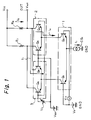
- a differential amplifier 1 is formed by two NPN type transistors Q 1 and Q 2 having a common emitter connected via a constant current source IS 1 whose current is I 1 , to a ground terminal GND.
- An AC input voltage V in is applied between bases of the transistors Q 1 and Q 2 .
- the differential amplifier 1 amplifiers the input voltage V in .
- a differential amplifier 2 is formed by two NPN type transistors Q 3 and Q 4 having a common emitter connected to the collector of the transistor Q 2 of the differential amplifier 1.
- a differential amplifier 3 is formed by two NPN type transistors Q 5 and Q 6 having a common emitter connected to the collector of the transistor Q 1 of the differential amplifier 1.
- the collectors of the transistors Q 3 and Q 4 are connected by way of a load resistor R 1 to a power supply terminal V cc , while the collectors of the transistors Q 5 and Q 6 are connected by way of a load resistor R 2 to the power supply terminal V cc .
- the AC input voltage V in is biased by a DC voltage V 0 .
- a DC bias voltage V c0 is applied to the bases of the transistors Q 3 and Q 6
- a gain control voltage V c is applied to the bases of the transistors Q 4 and Q 5 .
- the load resistor R 2 provides an output voltage V out at an output terminal OUT.
- a current I 0 flowing through the resistor R 2 is formed by a positive phase current I + flowing through the transistor Q 4 of the differential amplifier 2 and the transistor Q 2 of the differential amplifier 1 and a negative phase current I - flowing through the transistor Q 6 of the differential amplifier 3 and the transistor Q 1 of the differential amplifier 1.
- the positive phase current I + is equal to the negative phase current I - .
- the positive phase current I + offsets the negative phase current I - , so that the output voltage V OUT includes only a DC component.
- the gain of the gain-variable amplifier of Fig. 1 is minimum.
- V c V cc - V c0 .
- collector currents of the transistors Q 2 , Q 4 and Q 6 are denoted by I c2 , I c4 and I c4 , respectively, and the base currents of the transistorss Q 2 , Q 4 and Q 6 are denoted by I B2 , I B4 and I B6 , respectiverly.
- I c2 I c4 + I B4
- V out V cc - (I 1 /2 - I B2 - I B4 ) ⁇ R 2
- collector currents of the transistors Q 2 , Q 4 and Q 6 are denoted by I c2 ', I c4 'and I c4 ', respectively, and the base currents of the transistors Q 2 , Q 4 and Q 6 are denoted by I B2 ', I B4 ' and I B6 ', respectiverly.
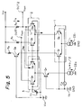
- Fig. 3 which illustrates a second prior art gain-variable amplifier (see JP-A-3-32209)
- the resistor R 1 of Fig. 1 is not present.
- the collectors of the transistors Q 1 , Q 3 and Q 5 of Fig. 1 are connected directly to the power supply terminal V cc .
- the common emitter of the transistors Q 5 and Q 6 of Fig. 1 are connected via a constant current source CS 2 whose current is I 2 , to the ground terminal GND. Note that the current ratio of I 1 to I 2 is 2.
- the load resistor R 2 also provides the output voltage V out at the output terminal OUT.
- the current I 0 flowing through the resistor R 2 is formed by a positive phase current I + flowing through the transistor Q 4 of the differential amplifier 2 and the transistor Q 2 of the differential amplifier 1 and a DC current I DC flowing through the transistor Q 6 of the differential amplifier 3 and the transistor Q 1 of the differential amplifier 1.
- the gain control voltage V c when the gain control voltage V c is negative, the DC current I DC is greater than the positive phase current I + . That is, the output voltage V out includes only a DC component. As a result, as shown in Fig. 4, the gain of the gain-variable amplifier of Fig. 3 is minimum.
- V c V cc - V c0 .
- collector currents of the transistors Q 2 , Q 4 and Q 6 are denoted by I c2 , I c4 and I c4 , respectively, and the base currents of the transistors Q 2 , Q 4 and Q 6 are denoted by I B2 , I B4 and I B6 , respectively.
- V out V cc - (I c4 + I c6 ) ⁇
- R 2 V cc - (I 1 /2 - I B4 ) ⁇ R 2
- collector currents of the transistors Q 2 , Q 4 and Q 6 are denoted by I c2 ', I c4 'and I c4 ', respectively, and the base currents of the transistorss Q 2 , Q 4 and Q 6 are denoted by I B2 ', I B4 ' and I B6 ', respectively.
- V out ' V cc - (I c4 ' + I c6 ') ⁇
- R 2 V cc - (I 1 /2 - I B6 ') ⁇ R 2 (9)
- the deviation of the DC component of the output voltage V out depending upon the gain control voltage V c is large.
- This large deviation can become enormous in the manufacture of integrated circuits due to deviations in the current amplification factor.
- the large deviation of the output DC voltage can be amplified by the downstream amplifiers which degrades various operating characteristics of the sets.
- the signal is subjected to distortion and degradation due to the difference in collector-emitter voltage V CE (V CE1 > V CE2 ) between the transistors Q 1 and Q 2 .
- V CE collector-emitter voltage
- the distortion appears as harmonic distortion of a transmitting/receiving frequency which degrades the operating characteristics.
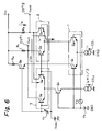
- an NPN type transistor Q 7 is interposed between the common emitter of the transistors Q 5 and Q 6 and the constant current source CS 2 of Fig. 3. Since the base of the transistor Q 7 is connected to the base of the transistor Q 1 , the transistor Q 7 corresponds to the transistor Q 1 . Also, a load resistor R 1 is interposed between the power supply terminal V cc and the collector of the transistor Q 3 of Fig. 3. The load resistor R 1 provides a negative phase output voltage V out1 at an output terminal OUT1, while the load resistor R 2 provides a positive phase output voltage V out2 at an output terminal OUT2.
- a load resistor R 3 and an NPN type transistor Q 8 are connected in series between the power supply terminal V cc and the collector of the transistor Q 1 of Fig. 3. Since the base of the transistor Q 8 is connected to the bases of the transistors Q 3 and Q 6 , the load resistor R 3 and the transistor Q 8 correspond to the load resistor R 1 and the transistor Q 3 (or Q 6 ), respectively.
- the gain characteristics of the gain-variable amplifier of Fig. 5 are the same as those of the gain-variable amplifier of Fig. 3 as shown in Fig. 4.
- collector currents of the transistors Q 2 , Q 4 , Q 6 and Q 7 are denoted by I c2 , I c4 , I c6 and I c7 , respectively
- base currents of the transistors Q 2 , Q 4 , Q 6 and Q 7 are denoted by I B2 , I B4 , I B6 and I B7 , respectively.
- V out2 V cc - (I c4 + I c6 ) ⁇
- R 2 V cc - (I 1 /2 - I B2 - I B4 ) ⁇ R 2
- collector currents of the transistors Q 2 , Q 4 , Q 6 and Q 7 are denoted by I c2 ', I c4 ', I c6 ' and I c7 ', respectively, and the base currents of the transistors Q 2 , Q 4 , Q 6 and Q 7 are denoted by I B2 ', I B4 ', I B6 ' and I B7 ' , respectively.
- V out2 ' V cc - (I c4 ' + I c6 ') ⁇ R 2
- the difference in the collector-emitter voltage V CE between the transistors Q 1 and Q 2 can be reduced by the resistor R 3 and the transistor Q 8 to minimize the distortion for the smallest gain.
- an NPN type transistor Q 7 is interposed between the common emitter of the transistors Q 5 and Q 6 and the constant current source CS 2 of Fig. 3. Since the base of the transistor Q 7 is connected to the base of the transistor Q 1 , the transistor Q 7 corresponds to the transistor Q 1 . Also, a load resistor R 1 is interposed between the power supply terminal V cc and the collector of the transistor Q 3 of Fig. 3. The load resistor R 1 provides a negative phase output voltage V out1 at an output terminal OUT1, while the load resistor R 2 provides a positive phase output voltage V out2 at an output terminal OUT2.
- a load resistor R 4 and an NPN type transistor Q 9 are connected in series between the power supply terminal V cc and the collector of the transistor Q 1 of Fig. 3. Since the base of the transistor Q 9 is connected to the base of the transistor Q 4 and Q 5 , the load resistor R 4 and the transistor Q 9 correspond to the load resistor R 2 and the transistor Q 4 (or Q 5 ), respectively.
- the gain characteristics of the gain-variable amplifier of Fig. 6 are also the same as those of the gain-variable amplifier of Fig. 3 as shown in Fig. 4.
- the DC output characteristics of the gain-variable amplifier of Fig. 6 are the same as those of the gain-variable amplifier of Fig. 5. That is, the in the gain-variable amplifier of Fig. 6, the deviation of the DC component of the output voltage V out2 depending upon the gain control voltage V c is zero.
- the difference in the collector-emitter voltage V CE between the transistors Q 1 and Q 2 can be reduced by the resistor R 4 and the transistor Q 9 to minimize the distortion for the largest gain.
- Fig. 6 which illustrates a third embodiment of the present invention
- the first embodiment as illustrated in Fig. 5 is combined with the second embodiment as illustrated in Fig. 6.
- the transistors Q 8 and Q 9 form a differential amplifier 4.
- the gain characteristics of the gain-variable amplifier of Fig. 7 are also the same as those of the gain-variable amplifier of Fig. 3 as shown in Fig. 4.
- the DC output characteristics of the gain-variable amplifier of Fig. 7 are the same as those of the gain-variable amplifier of Figs. 5 and 6. That is, the in the gain-variable amplifier of Fig. 7, the deviation of the DC component of the output voltage V out2 depending upon the gain control voltage V c is zero.
- the difference in the collector-emitter voltage V CE between the transistors Q 1 and Q 2 can be reduced by the resistors R 3 and R 4 and the transistors Q 8 and Q 9 to minimize the distortion regardless of the gain.
- the negative phase output voltage V out1 and the positive phase output voltage V out2 are both utilized.
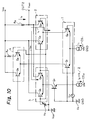
- the gain-variable amplifiers of Figs. 5, 6 and 7 can be modified into circuits as illustrated in Figs. 8, 9 and 10.
- the load resistors R 1 and R 3 of Fig. 5 are deleted; in Fig. 9, the load resistor R 1 of Fig. 6 is deleted; and in Fig. 10, the load resistors R 1 and R 3 are deleted.
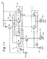
- the gain-variable amplifiers of Figs. 5, 6 and 7 can be modified into circuits as illustrated in Figs. 11, 12 and 13.
- the load resistor R 2 of Fig. 5 is deleted; in Fig. 12, the load resistors R 2 and R 4 of Fig. 6 are deleted; and in Fig. 13, the load resistors R 2 and R 4 are deleted.
- the deviation of the DC output characteristics can be reduced, and also, the distortion by the difference in the collector-emitter voltage between the input transistors can be reduced.
Landscapes
- Control Of Amplification And Gain Control (AREA)
- Amplifiers (AREA)
Applications Claiming Priority (3)
| Application Number | Priority Date | Filing Date | Title |
|---|---|---|---|
| JP168292/96 | 1996-06-07 | ||
| JP16829296 | 1996-06-07 | ||
| JP08168292A JP3097563B2 (ja) | 1996-06-07 | 1996-06-07 | 利得可変増幅器 |
Publications (3)
| Publication Number | Publication Date |
|---|---|
| EP0812063A2 true EP0812063A2 (de) | 1997-12-10 |
| EP0812063A3 EP0812063A3 (de) | 1999-06-16 |
| EP0812063B1 EP0812063B1 (de) | 2003-05-14 |
Family
ID=15865313
Family Applications (1)
| Application Number | Title | Priority Date | Filing Date |
|---|---|---|---|
| EP97109134A Expired - Lifetime EP0812063B1 (de) | 1996-06-07 | 1997-06-05 | Verstärker mit variabler Verstärkung und geringer Gleichspannungsabweichung am Ausgang und geringen Verzerrungen |
Country Status (4)
| Country | Link |
|---|---|
| US (1) | US5949285A (de) |
| EP (1) | EP0812063B1 (de) |
| JP (1) | JP3097563B2 (de) |
| DE (1) | DE69721898T2 (de) |
Families Citing this family (7)
| Publication number | Priority date | Publication date | Assignee | Title |
|---|---|---|---|---|
| EP0982848B1 (de) * | 1998-08-26 | 2002-10-30 | Nippon Telegraph and Telephone Corporation | Abgestimmter komplementärer Mischer |
| JP2000174576A (ja) * | 1998-12-08 | 2000-06-23 | Fujitsu Ltd | 可変利得増幅器 |
| US6968167B1 (en) * | 1999-10-21 | 2005-11-22 | Broadcom Corporation | Adaptive radio transceiver with calibration |
| US7555263B1 (en) * | 1999-10-21 | 2009-06-30 | Broadcom Corporation | Adaptive radio transceiver |
| US6684065B2 (en) * | 1999-12-20 | 2004-01-27 | Broadcom Corporation | Variable gain amplifier for low voltage applications |
| US6566951B1 (en) * | 2001-10-25 | 2003-05-20 | Lsi Logic Corporation | Low voltage variable gain amplifier having constant common mode DC output |
| KR100813464B1 (ko) * | 2006-11-24 | 2008-03-13 | (주)에프씨아이 | 저 전력 가변이득증폭기 |
Family Cites Families (9)
| Publication number | Priority date | Publication date | Assignee | Title |
|---|---|---|---|---|
| JPS57201311A (en) * | 1981-06-04 | 1982-12-09 | Toshiba Corp | Amplifier circuit |
| JPS59110211A (ja) * | 1982-12-15 | 1984-06-26 | Nec Corp | 利得制御回路 |
| JPS61152109A (ja) * | 1984-12-26 | 1986-07-10 | Hitachi Ltd | 制御回路 |
| JPS61157015A (ja) * | 1984-12-28 | 1986-07-16 | Mitsubishi Electric Corp | 可変利得増幅器 |
| JPS63244909A (ja) * | 1987-03-31 | 1988-10-12 | Toshiba Corp | 利得制御増幅器 |
| JPH02301307A (ja) * | 1989-05-16 | 1990-12-13 | Matsushita Electric Ind Co Ltd | ゲイン切替回路 |
| JPH077894B2 (ja) * | 1989-06-29 | 1995-01-30 | 日本電気株式会社 | 電圧制御増幅器 |
| JP3068903B2 (ja) * | 1991-08-29 | 2000-07-24 | 株式会社東芝 | ゲイン制御回路 |
| JPH0786854A (ja) * | 1993-09-17 | 1995-03-31 | Japan Radio Co Ltd | 自動利得制御増幅器 |
-
1996
- 1996-06-07 JP JP08168292A patent/JP3097563B2/ja not_active Expired - Fee Related
-
1997
- 1997-06-05 DE DE69721898T patent/DE69721898T2/de not_active Expired - Fee Related
- 1997-06-05 EP EP97109134A patent/EP0812063B1/de not_active Expired - Lifetime
- 1997-06-05 US US08/869,909 patent/US5949285A/en not_active Expired - Fee Related
Also Published As
| Publication number | Publication date |
|---|---|
| EP0812063A3 (de) | 1999-06-16 |
| DE69721898T2 (de) | 2004-05-19 |
| JPH09331220A (ja) | 1997-12-22 |
| US5949285A (en) | 1999-09-07 |
| JP3097563B2 (ja) | 2000-10-10 |
| EP0812063B1 (de) | 2003-05-14 |
| DE69721898D1 (de) | 2003-06-18 |
Similar Documents
| Publication | Publication Date | Title |
|---|---|---|
| JP2001358544A (ja) | 増幅回路 | |
| EP0812063A2 (de) | Verstärker mit variabler Verstärkung und geringer Gleichspannungsabweichung am Ausgang und geringen Verzerrungen | |
| US5682119A (en) | Variable gain circuit | |
| US20210218377A1 (en) | Amplifier with input bias current cancellation | |
| WO2004021560A1 (en) | System and method for establishing a bias current using a feedback loop | |
| WO2004021562A2 (en) | System and method for establishing the input impedance of an amplifier in a stacked configuration | |
| US5382919A (en) | Wideband constant impedance amplifiers | |
| US5357188A (en) | Current mirror circuit operable with a low power supply voltage | |
| JPS6117373B2 (de) | ||
| US6639469B2 (en) | Variable-gain amplifier circuit | |
| US6278299B1 (en) | Voltage to current converter | |
| CA1312359C (en) | Operational amplifier stages | |
| KR960004317B1 (ko) | Fm 수신기 | |
| EP1067677B1 (de) | Rundfunkfrequenzverstärker | |
| US5914637A (en) | Gain-variable amplifier with wide control range | |
| US6404285B1 (en) | Transistor amplifier that accommodates large input signals | |
| US6980052B1 (en) | Low-voltage pre-distortion circuit for linear-in-dB variable-gain cells | |
| US4167708A (en) | Transistor amplifier | |
| JPH045949B2 (de) | ||
| US20020097093A1 (en) | Compact variable gain amplifier | |
| US4330755A (en) | Power-amplifying circuit | |
| US20060049877A1 (en) | High frequency amplifier in an integrated circuit | |
| KR830001979B1 (ko) | 전력 증폭 회로 | |
| SU1713083A1 (ru) | Выходной каскад усилител мощности | |
| JPS6121857Y2 (de) |
Legal Events
| Date | Code | Title | Description |
|---|---|---|---|
| PUAI | Public reference made under article 153(3) epc to a published international application that has entered the european phase |
Free format text: ORIGINAL CODE: 0009012 |
|
| AK | Designated contracting states |
Kind code of ref document: A2 Designated state(s): DE GB |
|
| PUAL | Search report despatched |
Free format text: ORIGINAL CODE: 0009013 |
|
| AK | Designated contracting states |
Kind code of ref document: A3 Designated state(s): AT BE CH DE DK ES FI FR GB GR IE IT LI LU MC NL PT SE |
|
| 17P | Request for examination filed |
Effective date: 19990526 |
|
| AKX | Designation fees paid | ||
| RBV | Designated contracting states (corrected) |
Designated state(s): DE GB |
|
| REG | Reference to a national code |
Ref country code: DE Ref legal event code: 8566 |
|
| 17Q | First examination report despatched |
Effective date: 20010606 |
|
| GRAH | Despatch of communication of intention to grant a patent |
Free format text: ORIGINAL CODE: EPIDOS IGRA |
|
| GRAH | Despatch of communication of intention to grant a patent |
Free format text: ORIGINAL CODE: EPIDOS IGRA |
|
| GRAA | (expected) grant |
Free format text: ORIGINAL CODE: 0009210 |
|
| RAP1 | Party data changed (applicant data changed or rights of an application transferred) |
Owner name: NEC ELECTRONICS CORPORATION |
|
| AK | Designated contracting states |
Designated state(s): DE GB |
|
| REG | Reference to a national code |
Ref country code: GB Ref legal event code: FG4D |
|
| REF | Corresponds to: |
Ref document number: 69721898 Country of ref document: DE Date of ref document: 20030618 Kind code of ref document: P |
|
| PLBE | No opposition filed within time limit |
Free format text: ORIGINAL CODE: 0009261 |
|
| STAA | Information on the status of an ep patent application or granted ep patent |
Free format text: STATUS: NO OPPOSITION FILED WITHIN TIME LIMIT |
|
| 26N | No opposition filed |
Effective date: 20040217 |
|
| PGFP | Annual fee paid to national office [announced via postgrant information from national office to epo] |
Ref country code: DE Payment date: 20070531 Year of fee payment: 11 |
|
| PGFP | Annual fee paid to national office [announced via postgrant information from national office to epo] |
Ref country code: GB Payment date: 20070530 Year of fee payment: 11 |
|
| GBPC | Gb: european patent ceased through non-payment of renewal fee |
Effective date: 20080605 |
|
| PG25 | Lapsed in a contracting state [announced via postgrant information from national office to epo] |
Ref country code: DE Free format text: LAPSE BECAUSE OF NON-PAYMENT OF DUE FEES Effective date: 20090101 |
|
| PG25 | Lapsed in a contracting state [announced via postgrant information from national office to epo] |
Ref country code: GB Free format text: LAPSE BECAUSE OF NON-PAYMENT OF DUE FEES Effective date: 20080605 |