EP0812490B1 - Spannungsgesteuerter oszillator für hohe leistungen mit niedrigem rauschen - Google Patents
Spannungsgesteuerter oszillator für hohe leistungen mit niedrigem rauschen Download PDFInfo
- Publication number
- EP0812490B1 EP0812490B1 EP96908485A EP96908485A EP0812490B1 EP 0812490 B1 EP0812490 B1 EP 0812490B1 EP 96908485 A EP96908485 A EP 96908485A EP 96908485 A EP96908485 A EP 96908485A EP 0812490 B1 EP0812490 B1 EP 0812490B1
- Authority
- EP
- European Patent Office
- Prior art keywords
- vco
- active part
- noise
- buffer amplifier
- transistor
- Prior art date
- Legal status (The legal status is an assumption and is not a legal conclusion. Google has not performed a legal analysis and makes no representation as to the accuracy of the status listed.)
- Expired - Lifetime
Links
- 230000010355 oscillation Effects 0.000 claims abstract description 13
- 230000008878 coupling Effects 0.000 claims abstract description 7
- 238000010168 coupling process Methods 0.000 claims abstract description 7
- 238000005859 coupling reaction Methods 0.000 claims abstract description 7
- 230000002708 enhancing effect Effects 0.000 claims 2
- 230000001413 cellular effect Effects 0.000 abstract description 9
- 238000010897 surface acoustic wave method Methods 0.000 abstract description 7
- 238000001228 spectrum Methods 0.000 description 8
- 238000004891 communication Methods 0.000 description 6
- 239000000919 ceramic Substances 0.000 description 4
- 238000004088 simulation Methods 0.000 description 4
- 230000005540 biological transmission Effects 0.000 description 3
- 239000000969 carrier Substances 0.000 description 3
- 230000008901 benefit Effects 0.000 description 2
- 239000003990 capacitor Substances 0.000 description 2
- 230000010267 cellular communication Effects 0.000 description 2
- 238000010586 diagram Methods 0.000 description 2
- 230000000694 effects Effects 0.000 description 2
- 238000005516 engineering process Methods 0.000 description 2
- 230000006872 improvement Effects 0.000 description 2
- JBRZTFJDHDCESZ-UHFFFAOYSA-N AsGa Chemical compound [As]#[Ga] JBRZTFJDHDCESZ-UHFFFAOYSA-N 0.000 description 1
- 229910001218 Gallium arsenide Inorganic materials 0.000 description 1
- 230000018199 S phase Effects 0.000 description 1
- XUIMIQQOPSSXEZ-UHFFFAOYSA-N Silicon Chemical compound [Si] XUIMIQQOPSSXEZ-UHFFFAOYSA-N 0.000 description 1
- 238000006243 chemical reaction Methods 0.000 description 1
- 230000003247 decreasing effect Effects 0.000 description 1
- 230000008030 elimination Effects 0.000 description 1
- 238000003379 elimination reaction Methods 0.000 description 1
- 230000005669 field effect Effects 0.000 description 1
- 238000004519 manufacturing process Methods 0.000 description 1
- 238000010295 mobile communication Methods 0.000 description 1
- 238000012986 modification Methods 0.000 description 1
- 230000004048 modification Effects 0.000 description 1
- 230000004044 response Effects 0.000 description 1
- 229910052710 silicon Inorganic materials 0.000 description 1
- 239000010703 silicon Substances 0.000 description 1
- 230000003595 spectral effect Effects 0.000 description 1
Images



Classifications
-
- H—ELECTRICITY
- H03—ELECTRONIC CIRCUITRY
- H03B—GENERATION OF OSCILLATIONS, DIRECTLY OR BY FREQUENCY-CHANGING, BY CIRCUITS EMPLOYING ACTIVE ELEMENTS WHICH OPERATE IN A NON-SWITCHING MANNER; GENERATION OF NOISE BY SUCH CIRCUITS
- H03B5/00—Generation of oscillations using amplifier with regenerative feedback from output to input
- H03B5/18—Generation of oscillations using amplifier with regenerative feedback from output to input with frequency-determining element comprising distributed inductance and capacitance
-
- H—ELECTRICITY
- H03—ELECTRONIC CIRCUITRY
- H03B—GENERATION OF OSCILLATIONS, DIRECTLY OR BY FREQUENCY-CHANGING, BY CIRCUITS EMPLOYING ACTIVE ELEMENTS WHICH OPERATE IN A NON-SWITCHING MANNER; GENERATION OF NOISE BY SUCH CIRCUITS
- H03B5/00—Generation of oscillations using amplifier with regenerative feedback from output to input
- H03B5/18—Generation of oscillations using amplifier with regenerative feedback from output to input with frequency-determining element comprising distributed inductance and capacitance
- H03B5/1841—Generation of oscillations using amplifier with regenerative feedback from output to input with frequency-determining element comprising distributed inductance and capacitance the frequency-determining element being a strip line resonator
- H03B5/1847—Generation of oscillations using amplifier with regenerative feedback from output to input with frequency-determining element comprising distributed inductance and capacitance the frequency-determining element being a strip line resonator the active element in the amplifier being a semiconductor device
-
- H—ELECTRICITY
- H03—ELECTRONIC CIRCUITRY
- H03B—GENERATION OF OSCILLATIONS, DIRECTLY OR BY FREQUENCY-CHANGING, BY CIRCUITS EMPLOYING ACTIVE ELEMENTS WHICH OPERATE IN A NON-SWITCHING MANNER; GENERATION OF NOISE BY SUCH CIRCUITS
- H03B5/00—Generation of oscillations using amplifier with regenerative feedback from output to input
- H03B5/08—Generation of oscillations using amplifier with regenerative feedback from output to input with frequency-determining element comprising lumped inductance and capacitance
- H03B5/12—Generation of oscillations using amplifier with regenerative feedback from output to input with frequency-determining element comprising lumped inductance and capacitance active element in amplifier being semiconductor device
- H03B5/1203—Generation of oscillations using amplifier with regenerative feedback from output to input with frequency-determining element comprising lumped inductance and capacitance active element in amplifier being semiconductor device the amplifier being a single transistor
-
- H—ELECTRICITY
- H03—ELECTRONIC CIRCUITRY
- H03B—GENERATION OF OSCILLATIONS, DIRECTLY OR BY FREQUENCY-CHANGING, BY CIRCUITS EMPLOYING ACTIVE ELEMENTS WHICH OPERATE IN A NON-SWITCHING MANNER; GENERATION OF NOISE BY SUCH CIRCUITS
- H03B5/00—Generation of oscillations using amplifier with regenerative feedback from output to input
- H03B5/08—Generation of oscillations using amplifier with regenerative feedback from output to input with frequency-determining element comprising lumped inductance and capacitance
- H03B5/12—Generation of oscillations using amplifier with regenerative feedback from output to input with frequency-determining element comprising lumped inductance and capacitance active element in amplifier being semiconductor device
- H03B5/1231—Generation of oscillations using amplifier with regenerative feedback from output to input with frequency-determining element comprising lumped inductance and capacitance active element in amplifier being semiconductor device the amplifier comprising one or more bipolar transistors
-
- H—ELECTRICITY
- H03—ELECTRONIC CIRCUITRY
- H03B—GENERATION OF OSCILLATIONS, DIRECTLY OR BY FREQUENCY-CHANGING, BY CIRCUITS EMPLOYING ACTIVE ELEMENTS WHICH OPERATE IN A NON-SWITCHING MANNER; GENERATION OF NOISE BY SUCH CIRCUITS
- H03B5/00—Generation of oscillations using amplifier with regenerative feedback from output to input
- H03B5/08—Generation of oscillations using amplifier with regenerative feedback from output to input with frequency-determining element comprising lumped inductance and capacitance
- H03B5/12—Generation of oscillations using amplifier with regenerative feedback from output to input with frequency-determining element comprising lumped inductance and capacitance active element in amplifier being semiconductor device
- H03B5/1237—Generation of oscillations using amplifier with regenerative feedback from output to input with frequency-determining element comprising lumped inductance and capacitance active element in amplifier being semiconductor device comprising means for varying the frequency of the generator
- H03B5/124—Generation of oscillations using amplifier with regenerative feedback from output to input with frequency-determining element comprising lumped inductance and capacitance active element in amplifier being semiconductor device comprising means for varying the frequency of the generator the means comprising a voltage dependent capacitance
- H03B5/1243—Generation of oscillations using amplifier with regenerative feedback from output to input with frequency-determining element comprising lumped inductance and capacitance active element in amplifier being semiconductor device comprising means for varying the frequency of the generator the means comprising a voltage dependent capacitance the means comprising voltage variable capacitance diodes
-
- H—ELECTRICITY
- H03—ELECTRONIC CIRCUITRY
- H03B—GENERATION OF OSCILLATIONS, DIRECTLY OR BY FREQUENCY-CHANGING, BY CIRCUITS EMPLOYING ACTIVE ELEMENTS WHICH OPERATE IN A NON-SWITCHING MANNER; GENERATION OF NOISE BY SUCH CIRCUITS
- H03B2202/00—Aspects of oscillators relating to reduction of undesired oscillations
- H03B2202/03—Reduction of undesired oscillations originated from internal parasitic couplings, i.e. parasitic couplings within the oscillator itself
Definitions
- Applicant's invention relates to electronic oscillators and voltage-controlled oscillators.
- a voltage-controlled oscillator is a device for generating a signal having a frequency that can be varied in response to a control signal. Besides serving as stand-alone devices, VCOs are often components of phase-locked loops, voltage-to-frequency converters, etc.
- UK Patent Application GB-A-2 274 033 describes a voltage-controlled Colpitts oscillation circuit that includes a power supply terminal for supplying power to an oscillation stage, a buffer stage, and an output matching stage. Connected between the power supply terminal and ground is a high frequency bypass capacitor for bypassing electrical noise superimposed on the power supply to ground. A voltage feedback resistor is connected in series in a power supply line connected to the power supply terminal. The bypass capacitor and feedback resistor constitute a low-pass filter and have values determined so that the filter's cutoff frequency is at most a frequency f 0 .
- a conventional transmitter used in a cellular radio telephone or a portable terminal typically includes a VCO for generating a low-power carrier signal, a drive-stage amplifier, an inter-stage filter that may be either a ceramic or a surface-acoustic-wave (SAW) device, and a power amplifier for boosting the power of the carrier to the appropriate level.
- the drive-stage amplifier is needed to raise the VCO's low power output (typically 0 dBm or less) to a level appropriate for the power amplifier
- the inter-stage filter is needed to remove the noise produced by the drive-stage amplifier outside the spectral band of interest.
- the out-of-band noise power generated by the drive-stage amplifier is usually relatively high. If this noise power were to pass through the power amplifier, the amplified out-of-band noise power would be almost impossible to remove with commercially available filters that meet the requirements of the Electronic Industries Association (EIA). Hence, inter-stage filters are necessary in current, typical transmitters.
- EIA Electronic Industries Association
- Ceramic or SAW inter-stage filters are costly parts and are not suited for fabrication by current integrated circuit (IC) technology.
- IC integrated circuit
- a cellular transmitter can be implemented on a single IC chip, except for the ceramic or SAW inter-stage filter. Therefore, to reduce the transmitter's cost and to integrate the whole transmitter on a single IC chip, it is desirable to eliminate the inter-stage filter.
- One way to eliminate the inter-stage filter is to use a VCO having a higher power output.
- using a high-power VCO also permits elimination of the drive-stage amplifier, provided the noise power output of the high-power VCO is low.
- a VCO's noise power output is largely the result of two components: phase noise and amplitude noise.
- the noise far from the carrier is usually treated as amplitude-modulation (AM) noise.
- AM amplitude-modulation
- phase noise One of the most important characteristics of a VCO is the short-term frequency stability, or phase noise.
- noise sources that dominate the phase noise performance of a VCO are flicker noise, shot noise, and thermal noise of the VCO's active devices.
- the low-frequency noise, or 1/f noise modulates the signal generated by the VCO, forming noise side-bands that are spectrally very close to the carrier signal's frequency.
- the thermal noise contributes to the phase noise through a conversion from AM to phase modulation.
- VCOs are typically used for generating carrier signals in radio telephony.
- One current standards for cellular mobile telephone systems using analog frequency modulation (FM) of a radio-frequency (RF) carrier signal is the Advanced Mobile Phone Service (AMPS) system in the U.S. that uses wideband FM having a spacing of 30 KHz between carrier signals having frequencies around 900 MHz.
- AMPS Advanced Mobile Phone Service
- D-AMPS digital AMPS
- Some of the characteristics of the AMPS system are specified by the EIA/TIA-553 standard published by the Electronic Industries Association and Telecommunications Industry Association (EIA/TIA).
- a third analog-FM standard is the Total Access Communications System (TACS) in the United Kingdom that uses spacings of 25 KHz between carrier signals having frequencies around 900 MHz.
- a third analog-FM standard is the Nordic Mobile Telephone (NMT) system in Scandinavia that uses FM having spacings of 12.5 KHz between carriers in the 450-MHz and 900-MHz bands.
- a channel spacing of 10 KHz is achieved by splitting each 30-KHz-wide radio channel of an AMPS system into three parts.
- a radio channel is a bi-directional radio transmission path between two transceivers, and thus the channel comprises two carriers having different frequencies, one for uplink communication (mobile station to base station) and one for downlink communication (base station to mobile station).
- the frequency spacing between the two carriers of any radio channel is 45 MHz.
- D-AMPS digital AMPS
- TDMA time-division multiple access
- ADC American Digital Cellular System
- GSM Global System for Mobile Communications
- CDMA code division multiple access
- a circuit topology that results in a VCO having high output power and low noise using a low-Q resonator.
- a VCO comprises a resonant circuit; an active part that is connected to the resonant circuit and that includes at least one transistor connected in a Colpitts configuration; and a buffer amplifier, connected to the active part, for isolating the VCO from a load connected to the buffer amplifier.
- the active part includes capacitances connected in parallel with junction capacitances of the transistor, each capacitance having a value that is greater than a value of the respective junction capacitance with which it is connected in parallel, and a first resistance for providing negative feedback at low frequencies. Two of the capacitances enhance feedback in the active part at high frequencies and compensate for changes in the junction capacitances.
- the active part may include a plurality of transistors connected in parallel in a Colpitts configuration for reducing a value of a d.c. current passing through each respective transistor.
- the active part may further include a second resistance for reducing a gain of the active part when oscillation starts.
- the buffer amplifier is a linear amplifier including a transistor, and the active part and the buffer amplifier are connected by a capacitance for reducing coupling between the active part and the buffer amplifier.
- a VCO comprises a resonant circuit; an active part that is connected to the resonant circuit and that includes at least one transistor connected in a Colpitts configuration; a linear buffer amplifier, including a transistor, for isolating the VCO from a load connected to the buffer amplifier; and a capacitance for connecting the active part and the linear buffer amplifier and for reducing coupling between the active part and the buffer amplifier.
- the active part includes capacitances connected in parallel with junction capacitances of the transistor, each capacitance having a value that is greater than a value of the respective junction capacitance with which it is connected in parallel; a first resistance for providing negative feedback at low frequencies; and a second resistance for reducing a gain of the active part when oscillation starts.
- the active part may include a plurality of transistors connected in parallel in a Colpitts configuration for reducing a value of a d.c. current passing through each respective transistor.
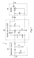
- FIG. 1 is an electrical schematic diagram of a VCO 1 in accordance with Applicant's invention that has a common, low-Q resonator for providing gain at the resonant frequency to an active part of the VCO.
- the VCO 1 comprises a resonator 10, an active part 20, and a buffer amplifier stage 30.
- the active part 20 is similar in some respects to a Colpitts oscillator, but the circuit 20 has significant additional components: capacitances C 3 , C 4 and resistance R 2 . The importance of these components and the advantages provided by them are explained below.
- phase noise dominates, while at frequencies very far from the output signal's frequency, AM noise dominates.
- AM noise dominates.
- the VCO's noise spectrum is a combination of phase noise and AM noise; which one is higher depends on the noise characteristics of the VCO's active and passive components, on how non-linear is the operation of the active devices, and on the circuit topology.
- the phase noise arises from low-frequency modulation of the output signal arising from the non-linear transconductance, g m , and non-linear junction capacitances, C bc , C bc , C ce , of the active part's transistor Q 1 . If the non-linear modulation on these non-linear elements is reduced, the phase noise is reduced accordingly.
- the active part 20 includes capacitances C 3 , C 4 that are connected in parallel with each non-linear junction capacitance.
- the linear capacitances C 3 , C 4 as well as conventional capacitance C 1 , reduce the non-linear modulation. To thieve optimum results, these capacitances should be selected such that C 3 > C bc and C 4 > C ce .
- “high” frequencies are frequencies that are at least approximately equal to the frequency of the carrier signal, i.e., the output signal generated by the VCO.
- “Low” frequencies are frequencies between d.c. (0 Hz) and about 100 KHz, for bipolar junction transistors (BJTs), or between d.c. and about 100 MHz, for field effect transistors (FETs).
- capacitances C 3 , C 4 Another benefit of using capacitances C 3 , C 4 is the improvement of pushing effect and temperature stability of the VCO 1 because the capacitances C 3 , C 4 reduce the effect of device capacitance changes with variation of supply voltage as well as variation of temperature.
- the VCO's performance may be further improved, if necessary, by selecting the Q-factor of the conventional resonator 10 to reduce the phase noise appropriately.
- the resonator 10 typically would have a Q-factor that is selected to be just sufficient for meeting the desired noise performance. It is believed a resonator 10 having a Q-factor of only about 100 is suitable for cellular telephony as described below.
- Resonator 10 can be constructed from a microstrip line 11 and a commercially available, low-cost varactor 12, such as those from Toko, Toshiba, and Alpha.
- the microstrip line can be replaced by a coaxial inductor, such as those that are commercially available from Trans-Tech.
- the bias voltage applied across the varactor 12, for example via a control signal terminal 13, can be used to control the frequency of the signal generated by the VCO 1, as can changes in the parameters of element 12. It will be appreciated that the coupling between the resonator 10 and the active part 20 should be reduced in order to increase the resonator's Q-factor.
- the active part 20 includes a resistance R 1 for introducing negative feedback at low frequencies to suppress the gain and noise at low frequencies while a capacitance C 2 maintains the gain at high frequencies, i.e., near the carrier frequency.
- a resistance R 1 for introducing negative feedback at low frequencies to suppress the gain and noise at low frequencies while a capacitance C 2 maintains the gain at high frequencies, i.e., near the carrier frequency.
- a low-noise VCO usually requires low d.c. bias current, so the VCO's output power is also low, and high-current operation for high output power results in high phase noise and AM noise.
- the transistor Q 1 may be implemented as two or more transistors connected in parallel. In this way, the d.c. current passing through each transistor is reduced (by half, if a pair of transistors are used), and as a result, the total noise level is lower than that of a single transistor Q 1 operating at the same output power level.
- BJTs such as silicon BJTs and gallium arsenide HBTs have lower 1/f noise than FETs such as MESFETs and HEMTs.
- FETs such as MESFETs and HEMTs.
- An application like a cellular radiotelephone transmitter might use two BJTs or three FETs.
- the resistance R 2 in conjunction with the other elements, such as capacitances C 3 , C 4 , C 2 , and C 1 reduces the gain at the moment oscillation starts.
- Applicant's VCO 1 also includes a buffer amplifier stage 30 for isolating the VCO from loading by the next stage connected to the buffer's output terminal 31, thereby avoiding any output signal frequency pulling due to changes in load impedance.
- the buffer amplifier 30 should operate as linearly as possible in order to avoid added noise from intermodulation arising in the buffer stage. It will be understood that the linear operation of the buffer amplifier 30 is determined by the operating point of the buffer's transistor Q2, and that operating point is determined by the transistor's d.c. bias and load impedance.
- the active part 20 and the buffer stage 30 are connected by a small capacitance C 6 having a capacitance value such that the coupling between the active part and the buffer stage is reduced and load-induced frequency pulling is reduced.
- VCO 1 has been simulated with a commercially available microwave/RF circuit simulator, HP-EEsof's J-Omega simulator, in conjunction with an HBT non-linear device model available from RF Micro Devices.
- the resonator circuit in the simulation had a loaded Q-factor (50-ohm load) of approximately 100.
- the simulation met expectations regarding output power level and phase noise near the carrier as well as the total noise power level in the receive band, 45 MHz away from the carrier. These expectations could not be met using conventional circuit topologies with the same resonator circuit.
- the simulated circuit provided more than 10 dB improvement in noise performance compared to conventional VCO circuits.
- the noise performance of a conventional VCO is usually specified only for close-in phase noise, i.e., phase noise at frequencies 25-30 KHz away from the carrier, depending on system bandwidth. Since Applicant's high power, low noise VCO eliminates the costly, bulky inter-stage filter, the VCO's noise performance must meet a further specification: noise power in the receive band.
- resistance R 1 could have a value between about 30 ohms and about 200 ohms
- resistance R 2 could have a value between about 2 ohms and about 10 ohms
- the d.c. current through transistor Q 1 could have a value between about 10 milliamps and 20 milliamps
- the d.c. current through transistor Q 2 could have a value between about 20 milliamps and 40 milliamps.
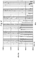
- Figure 2 shows the output power spectrum of the simulation.
- the output power level was +15.3 dBm at the fundamental frequency of the carrier, which was about 843 MHz, and was only about +0.9 dBm at the first harmonic (1686 MHz) of the carrier.
- Figure 3 shows the phase noise power spectrum of the simulation, where phase noise power level is plotted as a function of the logarithm of the frequency offset from the carrier signal's frequency. At 32 KHz away from the carrier, the phase noise power was less than -122.7 dBc/Hz, which is considerably better than the maximum acceptable phase noise level of -95 dBc/Hz. At 16 KHz frequency offset from the carrier, the phase noise power was -116.3 dBc/Hz. In addition, Figure 3 shows the phase noise level at 20 MHz away from the carrier was approximately -175 dBc/Hz, which is considerably better than the maximum acceptable phase noise level of -163 dBc/Hz in a GSM-standard cellular telephone system.
- Figure 4 shows the AM noise spectrum of the simulated VCO, where AM noise power level is plotted as a function of the logarithm of the frequency offset from the carrier signal's frequency. Comparing Figures 3 and 4 indicates the relative noise contributions from phase noise and AM noise.
- Figure 4 shows the AM noise power was -147.9 dBc/Hz at a 32 KHz frequency offset from the carrier, and -174.1 dBc/Hz at 44 MHz from the carrier.
- Figure 5 shows the combined phase-and-AM noise spectrum of the simulated VCO, where the combined noise power level is plotted as a function of the logarithm of the frequency offset from the carrier signal's frequency.
- Figure 5 shows that this noise power level was -163.1 dBm/Hz at 44 MHz frequency offset from the carrier, which is less than the maximum level of -160 dBm/Hz permitted by the AMPS specification.
- the best receive-band noise power level reached by simulating conventional VCO circuits was -150 dBm/Hz.
- Applicant's invention provides a new circuit topology for a high-power, low-noise VCO that can replace the driver-stage amplifier and the costly, high quality ceramic filter or SAW filter in a transmitter circuit. Because of its simplicity and the absence of a bulky filter, a VCO in accordance with Applicant's invention is easy to fabricate with a power amplifier on a single IC chip. Fabricating the VCO with the power amplifier on a single chip can significantly reduce product cost.
Landscapes
- Inductance-Capacitance Distribution Constants And Capacitance-Resistance Oscillators (AREA)
- Amplifiers (AREA)
Claims (8)
- Spannungsgesteuerter Oszillator (VCO) (1) mit hoher Leistung und mit niedrigem Rauschen, umfassend:wobei der aktive Teil Kapazitäten (C3, C4) enthält, die parallel geschaltet sind mit den Übergangskapazitäten (Cbc, Cce) des zumindest einen Transistors, wobei die Kapazitäten die Rückkopplung bei hohen Frequenzen verbessern, und jede Kapazität einen Wert hat, der größer ist als ein Wert der jeweiligen Übergangskapazität, mit welcher sie parallel geschaltet ist, und einen ersten Widerstand (R1) zur Bereitstellung einer negativen Rückkopplung, um die Verstärkung und ein Rauschen bei niedrigen Frequenzen zu unterdrücken, wobei die niedrigen Frequenzen weit entfernt liegen von der Oszillationsfrequenz des spannungsgesteuerten Oszillators.eine Resonanzschaltung (10, 11, 12);einen aktiven Teil (20), welcher mit der Resonanzschaltung verbunden ist, und welcher zumindest einen Transistor (Q1) umfaßt, der in einer Colpitts-Konfiguration angeschlossen ist; undeinen Pufferverstärker (30), der mit dem aktiven Teil verbunden ist, zur Isolierung des spannungsgesteuerten Oszillators von einer mit dem Pufferverstärker verbundenen Last;
- Spannungsgesteuerter Oszillator nach Anspruch 1, wobei zumindest zwei der Kapazitäten (C3, C4) Veränderungen in den Übergangskapazitäten (Cbc, Cce) kompensieren.
- Spannungsgesteuerter Oszillator nach Anspruch 1, wobei der aktive Teil (20) eine Vielzahl von Transistoren (Q1) umfaßt, die parallel in einer Colpitts-Konfiguration verbunden sind, zur Verringerung eines Wertes eines Gleichstroms, der durch jeden der Vielzahl der Transistoren fließt.
- Spannungsgesteuerter Oszillator nach Anspruch 1, wobei der aktive Teil (20) weiterhin einen zweiten Widerstand (R2) enthält, zur Verringerung einer Verstärkung des aktiven Teils, wenn die Oszillation beginnt.
- Spannungsgesteuerter Oszillator nach Anspruch 1, wobei der Pufferverstärker (30) ein linearer Verstärker ist, der einen Transistor (Q2) enthält.
- Spannungsgesteuerter Oszillator nach Anspruch 1, wobei der aktive Teil (20) und der Pufferverstärker (30) durch eine Kapazität (C6) verbunden sind, zur Verringerung der Kopplung zwischen dem aktiven Teil und dem Pufferverstärker.
- Spannungsgesteuerter Oszillator (1), umfassend:wobei der aktive Teil Kapazitäten (C3, C4) enthält, die parallel geschaltet sind mit Übergangskapazitäten (Cbc, Cce) des zumindest einen Transistors, wobei die Kapazitäten die Rückkopplung bei hohen Frequenzen verbessern, und jede Kapazität einen Wert hat, der größer ist als ein Wert der jeweiligen Übergangskapazität, mit welcher sie parallelgeschaltet ist; einen ersten Widerstand (R1) zur Bereitstellung einer negativen Rückkopplung, um die Verstärkung und das Rauschen bei niedrigen Frequenzen zu unterdrücken, wobei die niedrigen Frequenzen weit entfernt sind von der Oszillationsfrequenz des spannungsgesteuerten Oszillators, und einen zweiten Widersstand (R2) zur Verringerung einer Verstärkung des aktiven Teils, wenn die Oszillation beginnt.eine Resonanzschaltung (10, 11, 12);einen aktiven Teil (20), welcher mit der Resonanzschaltung verbunden ist, und welcher zumindest einen Transistor (Q1) enthält, der in einer Colpitts-Konfiguration angeschlossen ist;einen linearen Pufferverstärker (30), der einen Transistor (Q2) zur Isolierung des spannungsgesteuerten Oszillators von einer mit dem Pufferverstärker verbundenen Last enhält; undeine Kapazität (C6) zur Verbindung des aktiven Teils und des linearen Pufferverstärkers, und zur Verringerung der Kopplung zwischen dem aktiven Teil und dem Pufferverstärker;
- Spannungsgesteuerter Oszillator nach Anspruch 7, wobei der aktive Teil (20) eine Vielzahl von Transistoren (Q1) enthält, die parallel in einer Colpitts-Konfiguration geschaltet sind, zur Verringerung eines Wertes eines Gleichstroms, der durch jeden jeweiligen Transistor läuft.
Applications Claiming Priority (3)
| Application Number | Priority Date | Filing Date | Title |
|---|---|---|---|
| US395882 | 1995-02-28 | ||
| US08/395,882 US5714914A (en) | 1995-02-28 | 1995-02-28 | High-power low-noise voltage-controlled oscillator |
| PCT/US1996/002284 WO1996027234A1 (en) | 1995-02-28 | 1996-02-27 | High-power low-noise voltage-controlled oscillator |
Publications (2)
| Publication Number | Publication Date |
|---|---|
| EP0812490A1 EP0812490A1 (de) | 1997-12-17 |
| EP0812490B1 true EP0812490B1 (de) | 2000-04-19 |
Family
ID=23564934
Family Applications (1)
| Application Number | Title | Priority Date | Filing Date |
|---|---|---|---|
| EP96908485A Expired - Lifetime EP0812490B1 (de) | 1995-02-28 | 1996-02-27 | Spannungsgesteuerter oszillator für hohe leistungen mit niedrigem rauschen |
Country Status (10)
| Country | Link |
|---|---|
| US (1) | US5714914A (de) |
| EP (1) | EP0812490B1 (de) |
| JP (1) | JPH11502379A (de) |
| KR (1) | KR100355478B1 (de) |
| CN (1) | CN1068157C (de) |
| AU (1) | AU703377B2 (de) |
| BR (1) | BR9607059A (de) |
| CA (1) | CA2212752A1 (de) |
| DE (1) | DE69607834T2 (de) |
| WO (1) | WO1996027234A1 (de) |
Families Citing this family (22)
| Publication number | Priority date | Publication date | Assignee | Title |
|---|---|---|---|---|
| JP2001196854A (ja) * | 2000-01-07 | 2001-07-19 | Alps Electric Co Ltd | 電圧制御発振器 |
| KR100759508B1 (ko) | 2000-08-01 | 2007-09-18 | 정연문 | 귀환루프를 갖는 고주파 발진 회로 |
| US6549083B2 (en) * | 2000-08-11 | 2003-04-15 | Nihon Dempa Kogyo Co., Ltd. | High-frequency crystal oscillator outputting a harmonic component |
| US6462627B1 (en) * | 2000-08-25 | 2002-10-08 | Tropian Inc. | Oscillator circuit having reduced phase noise |
| US6545555B1 (en) | 2000-10-12 | 2003-04-08 | Telefonaktiebolaget, Lm Ericsson | Voltage controlled oscillator having a phase noise reduction device |
| US6661297B2 (en) * | 2000-12-20 | 2003-12-09 | Tektronix, Inc. | Multi-octave wideband voltage controlled oscillator |
| US6864758B2 (en) * | 2002-04-30 | 2005-03-08 | Freescale Semiconductor, Inc. | Apparatus and resonant circuit employing a varactor diode in parallel with a transmission line and method thereof |
| US7107261B2 (en) * | 2002-05-22 | 2006-09-12 | International Business Machines Corporation | Search engine providing match and alternative answer |
| US7068115B2 (en) * | 2002-09-13 | 2006-06-27 | Tlc Precision Wafer Technology, Inc. | Monolithic microwave integrated circuit voltage controlled coupled feedback oscillator |
| EP1418668A1 (de) * | 2002-11-07 | 2004-05-12 | Dialog Semiconductor GmbH | Hochgeschwindigkeitspufferverstärker mit hoher Isolation |
| JP2004236111A (ja) * | 2003-01-31 | 2004-08-19 | Murata Mfg Co Ltd | 電圧制御発振器、複合モジュールおよび通信装置 |
| US6967540B2 (en) * | 2003-03-06 | 2005-11-22 | Paratek Microwave, Inc. | Synthesizers incorporating parascan TM varactors |
| US20090093223A1 (en) * | 2007-10-05 | 2009-04-09 | Matsushita Electric Industrial Co., Ltd. | Methods and apparatus for reducing radiated field feedback in radio frequency transmitters |
| US8830007B1 (en) | 2012-03-19 | 2014-09-09 | Scientific Components Corporation | Ultra-low noise VCO |
| US8912854B2 (en) | 2013-01-04 | 2014-12-16 | International Business Machines Corporation | Structure for an inductor-capacitor voltage-controlled oscillator |
| US9917547B2 (en) * | 2013-01-09 | 2018-03-13 | Nxp Usa, Inc. | Voltage controlled oscillator |
| CN108667428B (zh) * | 2018-08-14 | 2024-07-23 | 广东工业大学 | 一种宽带压控振荡器 |
| CN110417352B (zh) * | 2019-08-26 | 2024-04-30 | 厦门英诺迅科技有限公司 | 一种稳定恒流偏置cascode mmic vco |
| WO2021183329A1 (en) * | 2020-03-11 | 2021-09-16 | Leco Corporation | Voltage stabilizer for sources with unacceptable output variation |
| CN112994617A (zh) * | 2021-04-13 | 2021-06-18 | 苏州英诺迅科技股份有限公司 | 一种改善频率温漂特性的振荡器电路结构 |
| CN114047796B (zh) * | 2022-01-12 | 2022-04-05 | 北京晨晶精仪电子有限公司 | 控温电路、恒温晶振电路及恒温晶体振荡器 |
| CN117713812B (zh) * | 2024-02-04 | 2024-04-26 | 安徽矽磊电子科技有限公司 | 一种用于锁相环的宽带振荡器 |
Family Cites Families (11)
| Publication number | Priority date | Publication date | Assignee | Title |
|---|---|---|---|---|
| US4134085A (en) * | 1977-05-31 | 1979-01-09 | Driscoll Michael M | Narrow deviation voltage controlled crystal oscillator for mobile radio |
| JPS58200606A (ja) * | 1982-05-17 | 1983-11-22 | Sharp Corp | 発振回路 |
| US4511861A (en) * | 1982-11-15 | 1985-04-16 | General Electric Company | VCO Having field effect and bipolar transistors in parallel |
| JPS60190004A (ja) * | 1984-03-09 | 1985-09-27 | Matsushita Electric Ind Co Ltd | 発振回路 |
| US4571557A (en) * | 1984-03-26 | 1986-02-18 | Randy Brandt | Wide band transistor oscillator |
| US4795988A (en) * | 1986-11-18 | 1989-01-03 | Britz William J | Low distortion oscillator |
| US5122763A (en) * | 1989-08-25 | 1992-06-16 | Anritsu Corporation | Frequency snythesizer for implementing generator of highly pure signals and circuit devices, such as vcq, bll and sg, used therein |
| US5130674A (en) * | 1991-09-30 | 1992-07-14 | Motorola, Inc. | Voltage controlled oscilator having controlled bias voltage, AGC and output amplifier |
| US5144264A (en) * | 1991-11-01 | 1992-09-01 | Motorola, Inc. | Wideband voltage controlled oscillator having open loop gain compensation |
| US5352993A (en) * | 1992-09-30 | 1994-10-04 | Telefonaktiebolaget L M Ericsson | Voltage controlled saw oscillator |
| JPH06188729A (ja) * | 1992-12-16 | 1994-07-08 | Murata Mfg Co Ltd | ノイズ除去回路および電圧制御形発振回路 |
-
1995
- 1995-02-28 US US08/395,882 patent/US5714914A/en not_active Expired - Lifetime
-
1996
- 1996-02-27 EP EP96908485A patent/EP0812490B1/de not_active Expired - Lifetime
- 1996-02-27 AU AU51709/96A patent/AU703377B2/en not_active Ceased
- 1996-02-27 CA CA002212752A patent/CA2212752A1/en not_active Abandoned
- 1996-02-27 CN CN96192228A patent/CN1068157C/zh not_active Expired - Fee Related
- 1996-02-27 WO PCT/US1996/002284 patent/WO1996027234A1/en not_active Ceased
- 1996-02-27 BR BR9607059A patent/BR9607059A/pt not_active IP Right Cessation
- 1996-02-27 KR KR1019970705961A patent/KR100355478B1/ko not_active Expired - Fee Related
- 1996-02-27 JP JP8526314A patent/JPH11502379A/ja not_active Ceased
- 1996-02-27 DE DE69607834T patent/DE69607834T2/de not_active Expired - Fee Related
Also Published As
| Publication number | Publication date |
|---|---|
| JPH11502379A (ja) | 1999-02-23 |
| MX9706312A (es) | 1997-11-29 |
| DE69607834D1 (de) | 2000-05-25 |
| DE69607834T2 (de) | 2000-10-19 |
| US5714914A (en) | 1998-02-03 |
| KR100355478B1 (ko) | 2002-11-18 |
| AU703377B2 (en) | 1999-03-25 |
| WO1996027234A1 (en) | 1996-09-06 |
| AU5170996A (en) | 1996-09-18 |
| CN1176711A (zh) | 1998-03-18 |
| EP0812490A1 (de) | 1997-12-17 |
| BR9607059A (pt) | 1998-06-09 |
| CN1068157C (zh) | 2001-07-04 |
| KR19980702555A (ko) | 1998-07-15 |
| CA2212752A1 (en) | 1996-09-06 |
Similar Documents
| Publication | Publication Date | Title |
|---|---|---|
| EP0812490B1 (de) | Spannungsgesteuerter oszillator für hohe leistungen mit niedrigem rauschen | |
| US6731182B2 (en) | Voltage-controlled oscillator and communication apparatus employing the same | |
| US6259901B1 (en) | Radio-frequency power amplifier of mobile communication equipment | |
| US6680657B2 (en) | Cross-coupled voltage controlled oscillator with improved phase noise performance | |
| US6833769B2 (en) | Voltage controlled capacitive elements having a biasing network | |
| US8618884B2 (en) | High-frequency signal processing device | |
| WO2003005568A1 (en) | Radio frequency power amplifier for cellular telephones | |
| US20030045252A1 (en) | Power amplifier | |
| JPH05275924A (ja) | 高周波発振回路 | |
| US6784753B2 (en) | Method for modulating an output voltage of a RF transmitter circuit, and RF transmitter circuit | |
| CN115088191A (zh) | 功率放大电路、高频电路以及通信装置 | |
| US6577189B2 (en) | Scheme for reducing transmit-band noise floor and adjacent channel power with power backoff | |
| US5621362A (en) | Cascode oscillator having optimum phase noise and bandwidth performance | |
| US6271737B1 (en) | Communication device with feedback for cancellation of perturbations | |
| US6593819B2 (en) | Low phase noise dual band voltage controlled oscillator | |
| US5859573A (en) | Circuit for separating the output of an oscillator from the other parts of a mobile communication system | |
| Woo et al. | A fully integrated transceiver chip for the 900 MHz communication bands | |
| Han et al. | A fully integrated receiver front-end reconfigured by PLL | |
| JP2001267845A (ja) | 電圧制御発振器 | |
| JP2006166089A (ja) | 高周波電力増幅器 | |
| JPH11331297A (ja) | ディジタル信号変調装置 | |
| MXPA97006312A (en) | Oscillator controlled by voltage, low noise, and high poten | |
| CA2533623A1 (en) | Tunable oscillator |
Legal Events
| Date | Code | Title | Description |
|---|---|---|---|
| PUAI | Public reference made under article 153(3) epc to a published international application that has entered the european phase |
Free format text: ORIGINAL CODE: 0009012 |
|
| 17P | Request for examination filed |
Effective date: 19970716 |
|
| AK | Designated contracting states |
Kind code of ref document: A1 Designated state(s): DE FR GB IT SE |
|
| GRAG | Despatch of communication of intention to grant |
Free format text: ORIGINAL CODE: EPIDOS AGRA |
|
| 17Q | First examination report despatched |
Effective date: 19990505 |
|
| GRAG | Despatch of communication of intention to grant |
Free format text: ORIGINAL CODE: EPIDOS AGRA |
|
| GRAH | Despatch of communication of intention to grant a patent |
Free format text: ORIGINAL CODE: EPIDOS IGRA |
|
| GRAH | Despatch of communication of intention to grant a patent |
Free format text: ORIGINAL CODE: EPIDOS IGRA |
|
| GRAA | (expected) grant |
Free format text: ORIGINAL CODE: 0009210 |
|
| AK | Designated contracting states |
Kind code of ref document: B1 Designated state(s): DE FR GB IT SE |
|
| REF | Corresponds to: |
Ref document number: 69607834 Country of ref document: DE Date of ref document: 20000525 |
|
| ET | Fr: translation filed | ||
| ITF | It: translation for a ep patent filed | ||
| PLBE | No opposition filed within time limit |
Free format text: ORIGINAL CODE: 0009261 |
|
| STAA | Information on the status of an ep patent application or granted ep patent |
Free format text: STATUS: NO OPPOSITION FILED WITHIN TIME LIMIT |
|
| 26N | No opposition filed | ||
| REG | Reference to a national code |
Ref country code: GB Ref legal event code: IF02 |
|
| PGFP | Annual fee paid to national office [announced via postgrant information from national office to epo] |
Ref country code: FR Payment date: 20060217 Year of fee payment: 11 |
|
| PG25 | Lapsed in a contracting state [announced via postgrant information from national office to epo] |
Ref country code: SE Free format text: LAPSE BECAUSE OF NON-PAYMENT OF DUE FEES Effective date: 20070228 |
|
| EUG | Se: european patent has lapsed | ||
| REG | Reference to a national code |
Ref country code: FR Ref legal event code: ST Effective date: 20071030 |
|
| PGFP | Annual fee paid to national office [announced via postgrant information from national office to epo] |
Ref country code: SE Payment date: 20060227 Year of fee payment: 11 |
|
| PG25 | Lapsed in a contracting state [announced via postgrant information from national office to epo] |
Ref country code: FR Free format text: LAPSE BECAUSE OF NON-PAYMENT OF DUE FEES Effective date: 20070228 |
|
| PGFP | Annual fee paid to national office [announced via postgrant information from national office to epo] |
Ref country code: IT Payment date: 20080227 Year of fee payment: 13 |
|
| PGFP | Annual fee paid to national office [announced via postgrant information from national office to epo] |
Ref country code: GB Payment date: 20090227 Year of fee payment: 14 |
|
| PGFP | Annual fee paid to national office [announced via postgrant information from national office to epo] |
Ref country code: DE Payment date: 20090331 Year of fee payment: 14 |
|
| GBPC | Gb: european patent ceased through non-payment of renewal fee |
Effective date: 20100227 |
|
| PG25 | Lapsed in a contracting state [announced via postgrant information from national office to epo] |
Ref country code: DE Free format text: LAPSE BECAUSE OF NON-PAYMENT OF DUE FEES Effective date: 20100901 |
|
| PG25 | Lapsed in a contracting state [announced via postgrant information from national office to epo] |
Ref country code: IT Free format text: LAPSE BECAUSE OF NON-PAYMENT OF DUE FEES Effective date: 20090227 Ref country code: GB Free format text: LAPSE BECAUSE OF NON-PAYMENT OF DUE FEES Effective date: 20100227 |