EP0813093B1 - Optische Wellenleitervorrichtung - Google Patents
Optische Wellenleitervorrichtung Download PDFInfo
- Publication number
- EP0813093B1 EP0813093B1 EP97304044A EP97304044A EP0813093B1 EP 0813093 B1 EP0813093 B1 EP 0813093B1 EP 97304044 A EP97304044 A EP 97304044A EP 97304044 A EP97304044 A EP 97304044A EP 0813093 B1 EP0813093 B1 EP 0813093B1
- Authority
- EP
- European Patent Office
- Prior art keywords
- optical waveguide
- antistatic film
- substrate
- waveguide device
- electrode
- Prior art date
- Legal status (The legal status is an assumption and is not a legal conclusion. Google has not performed a legal analysis and makes no representation as to the accuracy of the status listed.)
- Expired - Lifetime
Links
- 230000003287 optical effect Effects 0.000 title claims description 70
- 239000000758 substrate Substances 0.000 claims description 42
- 230000008646 thermal stress Effects 0.000 claims description 16
- 239000010936 titanium Substances 0.000 claims description 14
- 239000000463 material Substances 0.000 claims description 11
- 229910052719 titanium Inorganic materials 0.000 claims description 7
- 238000009792 diffusion process Methods 0.000 claims description 6
- 230000005693 optoelectronics Effects 0.000 claims description 6
- 230000010287 polarization Effects 0.000 claims description 6
- RTAQQCXQSZGOHL-UHFFFAOYSA-N Titanium Chemical compound [Ti] RTAQQCXQSZGOHL-UHFFFAOYSA-N 0.000 claims description 4
- 229910052782 aluminium Inorganic materials 0.000 claims description 3
- 229910052787 antimony Inorganic materials 0.000 claims description 3
- 229910052785 arsenic Inorganic materials 0.000 claims description 3
- 229910052796 boron Inorganic materials 0.000 claims description 3
- 150000001875 compounds Chemical class 0.000 claims description 3
- 229910052733 gallium Inorganic materials 0.000 claims description 3
- 229910052732 germanium Inorganic materials 0.000 claims description 3
- 229910052738 indium Inorganic materials 0.000 claims description 3
- 229910052710 silicon Inorganic materials 0.000 claims description 3
- 229910052718 tin Inorganic materials 0.000 claims description 3
- GQYHUHYESMUTHG-UHFFFAOYSA-N lithium niobate Chemical compound [Li+].[O-][Nb](=O)=O GQYHUHYESMUTHG-UHFFFAOYSA-N 0.000 claims description 2
- 230000008859 change Effects 0.000 description 20
- 230000005684 electric field Effects 0.000 description 13
- 230000035882 stress Effects 0.000 description 8
- 238000000034 method Methods 0.000 description 6
- 230000000694 effects Effects 0.000 description 5
- VYPSYNLAJGMNEJ-UHFFFAOYSA-N Silicium dioxide Chemical compound O=[Si]=O VYPSYNLAJGMNEJ-UHFFFAOYSA-N 0.000 description 4
- 230000008569 process Effects 0.000 description 4
- 230000009467 reduction Effects 0.000 description 4
- 229910003327 LiNbO3 Inorganic materials 0.000 description 3
- 230000005540 biological transmission Effects 0.000 description 3
- 238000009713 electroplating Methods 0.000 description 3
- 238000004519 manufacturing process Methods 0.000 description 3
- 229920002120 photoresistant polymer Polymers 0.000 description 3
- 230000015572 biosynthetic process Effects 0.000 description 2
- 229910052681 coesite Inorganic materials 0.000 description 2
- 238000004891 communication Methods 0.000 description 2
- 229910052906 cristobalite Inorganic materials 0.000 description 2
- 239000013078 crystal Substances 0.000 description 2
- 230000003247 decreasing effect Effects 0.000 description 2
- 229910052737 gold Inorganic materials 0.000 description 2
- 239000012535 impurity Substances 0.000 description 2
- 229910052751 metal Inorganic materials 0.000 description 2
- 239000002184 metal Substances 0.000 description 2
- 238000000059 patterning Methods 0.000 description 2
- 239000000377 silicon dioxide Substances 0.000 description 2
- 238000004544 sputter deposition Methods 0.000 description 2
- 229910052682 stishovite Inorganic materials 0.000 description 2
- 229910052905 tridymite Inorganic materials 0.000 description 2
- 238000010521 absorption reaction Methods 0.000 description 1
- 239000000853 adhesive Substances 0.000 description 1
- 230000001070 adhesive effect Effects 0.000 description 1
- 230000002411 adverse Effects 0.000 description 1
- 238000003486 chemical etching Methods 0.000 description 1
- 238000010668 complexation reaction Methods 0.000 description 1
- 230000006835 compression Effects 0.000 description 1
- 238000007906 compression Methods 0.000 description 1
- 230000001276 controlling effect Effects 0.000 description 1
- 238000010586 diagram Methods 0.000 description 1
- 238000001312 dry etching Methods 0.000 description 1
- 239000000835 fiber Substances 0.000 description 1
- 239000003292 glue Substances 0.000 description 1
- 230000010365 information processing Effects 0.000 description 1
- 230000010354 integration Effects 0.000 description 1
- 238000011835 investigation Methods 0.000 description 1
- 230000007246 mechanism Effects 0.000 description 1
- 238000012986 modification Methods 0.000 description 1
- 230000004048 modification Effects 0.000 description 1
- 239000013307 optical fiber Substances 0.000 description 1
- 239000003960 organic solvent Substances 0.000 description 1
- 230000001105 regulatory effect Effects 0.000 description 1
- 230000000087 stabilizing effect Effects 0.000 description 1
Images




Classifications
-
- G—PHYSICS
- G02—OPTICS
- G02F—OPTICAL DEVICES OR ARRANGEMENTS FOR THE CONTROL OF LIGHT BY MODIFICATION OF THE OPTICAL PROPERTIES OF THE MEDIA OF THE ELEMENTS INVOLVED THEREIN; NON-LINEAR OPTICS; FREQUENCY-CHANGING OF LIGHT; OPTICAL LOGIC ELEMENTS; OPTICAL ANALOGUE/DIGITAL CONVERTERS
- G02F1/00—Devices or arrangements for the control of the intensity, colour, phase, polarisation or direction of light arriving from an independent light source, e.g. switching, gating or modulating; Non-linear optics
- G02F1/01—Devices or arrangements for the control of the intensity, colour, phase, polarisation or direction of light arriving from an independent light source, e.g. switching, gating or modulating; Non-linear optics for the control of the intensity, phase, polarisation or colour
- G02F1/03—Devices or arrangements for the control of the intensity, colour, phase, polarisation or direction of light arriving from an independent light source, e.g. switching, gating or modulating; Non-linear optics for the control of the intensity, phase, polarisation or colour based on ceramics or electro-optical crystals, e.g. exhibiting Pockels effect or Kerr effect
- G02F1/035—Devices or arrangements for the control of the intensity, colour, phase, polarisation or direction of light arriving from an independent light source, e.g. switching, gating or modulating; Non-linear optics for the control of the intensity, phase, polarisation or colour based on ceramics or electro-optical crystals, e.g. exhibiting Pockels effect or Kerr effect in an optical waveguide structure
- G02F1/0356—Devices or arrangements for the control of the intensity, colour, phase, polarisation or direction of light arriving from an independent light source, e.g. switching, gating or modulating; Non-linear optics for the control of the intensity, phase, polarisation or colour based on ceramics or electro-optical crystals, e.g. exhibiting Pockels effect or Kerr effect in an optical waveguide structure controlled by a high-frequency electromagnetic wave component in an electric waveguide structure
-
- G—PHYSICS
- G02—OPTICS
- G02F—OPTICAL DEVICES OR ARRANGEMENTS FOR THE CONTROL OF LIGHT BY MODIFICATION OF THE OPTICAL PROPERTIES OF THE MEDIA OF THE ELEMENTS INVOLVED THEREIN; NON-LINEAR OPTICS; FREQUENCY-CHANGING OF LIGHT; OPTICAL LOGIC ELEMENTS; OPTICAL ANALOGUE/DIGITAL CONVERTERS
- G02F2203/00—Function characteristic
- G02F2203/21—Thermal instability, i.e. DC drift, of an optical modulator; Arrangements or methods for the reduction thereof
Definitions
- the present invention relates to an optical waveguide device having an optical waveguide and electrodes for controlling a guided lightwave which are formed on a surface of a substrate which has an electrooptical effect, and more particularly to an improved optical waveguide device which can be operated stably against an ambient temperature change and the properties of the optical modulator are not affected by unevenness in electric conductivity of antistatic films for preventing unstable operation by pyroelectrically induced charge or the like.
- the present invention also relates to an optical waveguide device which is capable of a high speed operation and utilizes a substrate with an electrooptical effect, more specifically to a constitution for optical intensity modulators, optical phase modulators, polarization scramblers or the like which improves properties of long-distance optical fiber transmission.
- optical waveguide devices are studied as the key device. Since a lightwave is confined in a waveguide in an optical waveguide device, a high speed operation is possible and miniaturization, integration, complexation and the like can be easily attained. Furthermore, it has also been investigated to apply an optical waveguide device to optical measuring instruments, optical information processing or the like.
- optical waveguide devices those having an optical waveguide formed by effecting a thermal diffusion of titanium (Ti) into a ferroelectric substrate such as LiNbO 3 (hereinafter simply referred to as LN) which has a large electrooptical effect are known and various investigations have been made on them.
- LN ferroelectric substrate
- the optical modulator For an optical modulator utilizing such LN waveguide, it is relatively easy to suppress optical losses.
- the optical modulator would have a modulation bandwidth of 10 GHz or more by constituting a hot electrode as a traveling-wave type electrode and thus, it is considered as a key device for realizing an super-high speed optical communication system.
- Fig. 4 of the accompanying drawings is a perspective view showing a waveguide-type optical phase modulator as an example of Ti-diffused, LN waveguide-type optical modulators.
- Ti is diffused into a surface of Z-cut LN substrate and traveling-wave type electrodes are formed thereon.
- a buffer layer which is, for example, composed of SiO 2 is formed between a waveguide and the electrodes in order to prevent a guided lightwave from being absorbed in the metal electrodes.
- an incident lightwave is polarized only in one direction using a laminated micropolarizer lamipole (11), since the LN substrate is a large anisotropic crystal.
- the guided lightwave interacts with an electric field occurring due to a microwave (electric signals) applied by a signal source (7), thereby changing the phase of guided lightwave.
- the electrodes are generally formed as a thick film in those modulators having traveling-wave type electrodes.
- broadening of the bandwidth is attained by matching the propagation velocity of the guided lightwave with the velocity of the microwave traveling across the electrodes, namely by velocity matching between the guided lightwave and the microwave.
- thick film electrodes are formed by an electroplating process.
- waveguide-type optical phase modulators In addition to waveguide-type optical phase modulators, one example of which has been explained so far, mention may be made of branched interferometric-type optical intensity modulators in which two Y-branch waveguides are combined, as well as to polarization scramblers wherein a polarizer is arranged on the incident side of the optical phase modulator at an angle of 45 degrees with respect to the crystallographic axis.
- ferroelectric material Since a ferroelectric material is used as the substrate in these devices, they are likely to be pyroelectrically charged due to ambient temperature change, and operation of the device becomes unstable because of such pyroelectrically induced charge.
- Fig. 5a there is shown a structure in which no antistatic film is formed.
- an electric field caused by induced charges on the surface of a substrate (6) changes the refractive index of a waveguide (3), and thus properties of the modulator become unstable with respect to ambient temperature change.
- the above-mentioned two constitutions have such a common feature that the antistatic film (5) is always in contact with both of the hot electrode (1) and the ground electrode (2).
- This feature is aimed to uniformly distribute the charges induced in the surface of the substrate between the electrodes, and is considered to be necessary for preventing unstableness in operation of the device.
- the pyroelectric charge is not the only cause for unstableness in operation of the device.
- the electrode films which are formed thickly for broadening the bandwidth of the device have a quite large stress. Since this stress fluctuates in accordance with temperature change, an operating point of the device may be shifted via the photoelastic effect of the LN substrate.
- other stresses such as thermal stress of the buffer layer formed on the surface of the substrate also act on the waveguide through the photoelastic effect of the substrate, thereby shifting the operating point. Accordingly, even a constitution in which an antistatic film is formed all over the surface of the substrate involves such a problem that the device cannot be operated stably against the ambient temperature change.
- ITO and Si are generally used for the antistatic film (5), but the electric conductivity of these materials is greatly affected by a very small difference in contained impurities or manufacturing conditions (it easily changes by several hundred times to several thousand times). Since such film is in contact with both the hot electrode (1) and the ground electrode (2), the resistance between the electrodes of the modulator may be greatly changed, thereby causing fluctuations in electrical properties.
- An object of the present invention is to solve the above-mentioned problems and to provide an optical waveguide device with excellent temperature properties wherein fluctuations in electrical properties of the modulator as well as reduction of electric field by applied microwave are effectively suppressed.
- an optical waveguide device which comprises: an optical waveguide for guiding a lightwave; at least a pair of electrodes composed of a hot electrode and a ground electrode which control a guided lightwave; a buffer layer formed between the electrodes and the optical waveguide, on a surface of a substrate having an electrooptical effect; and an antistatic film formed on an upper surface of the buffer layer such that it comes into contact with the hot electrode.
- the substrate, on which the optical waveguide is formed is made of lithium niobate (LiNbO 3 ) and the optical waveguide is formed by effecting a thermal diffusion of titanium (Ti).
- LiNbO 3 lithium niobate
- Ti titanium
- the antistatic film which is in contact with the hot electrode, is preferably composed of a semiconductive material.
- the antistatic film is made of a material selected from the group consisting of Ga, In, As, Al, B, Ge, Si, Sn and Sb or a compound thereof.
- the gap (g) between the antistatic film and the ground electrode is preferably set at such a value that is larger than zero and smaller than a distance (S) between the electrodes.
- the optical waveguide device according to the present invention is characterized in that the gap (g) between the antistatic film and the ground electrode is regulated such that it is possible to compensate a shift of operating point due to the thermal stress of the optical waveguide device with a shift of operating point due to an electric charge induced in a region of the substrate located right under the gap (g).
- the optical waveguide device is preferably an intensity modulator or a phase modulator or a polarization scrambler.
- the antistatic film (5) comes into contact only with the hot electrode (1) and is not in contact with the ground electrode (2). In addition, there is absolutely no antistatic film (5) between the ground electrode (2) and the buffer layer (4).
- the gap (g) between the antistatic film (5) and the ground electrode (2) is adjusted so that it is possible to compensate a shift of operating point due to the thermal stress of the optical waveguide device with a shift of operating point due to an electric charge induced in a region of the substrate (6) located right under the gap (g) in the optical waveguide device according to the present invention.
- the device of the present invention is different from the conventional devices in that the antistatic film (5) neither comes into contact with both of the hot electrode (1) and the ground electrode (2) nor exists on the entire surface between the electrodes (1), (2) and the buffer layer (4) and the gap (g) between the antistatic film (5) and the ground electrode (2) is adjusted to as to compensate a shift of operating point due to the thermal stress of the device with a shift of operating point due to an electric charge induced in a region of the substrate (6) located under the gap (g).
- the antistatic film (5) whose electric conductivity is greatly affected by a very small difference in contained impurities or manufacturing conditions, may cause fluctuations in electrical properties of the optical modulators.
- the antistatic film (5) may be arranged such that it does not extend so far as to contact with the ground electrode (2) as shown in Fig. 1. Due to such a constitution, in other words, since the antistatic film (5) is not in contacted state between the hot electrode (1) and the ground electrode (2), the resistance between the electrodes of the optical modulator is remarkably more stable and thus the electrical properties thereof are less influenced when compared with the case where the antistatic film (5) is in contact with both the hot electrode (1) and the ground electrode (2) even when the electric conductivity of the antistatic film (5) fluctuates.
- the present invention solves this problem by constituting the optical waveguide device such that the shift of operating point due to the thermal stress and the shift of operating point due to the electric charge would compensate each other.
- Fig. 6 there are shown respective examples of shifting of the operation point due to thermal stress occurred in accordance with the temperature change and the shifting of the operation point due to electric charge induced in accordance with the temperature change.
- Magnitude and direction (whether it shifts toward the plus direction or toward the minus direction) of the shifting of the operating point caused by the thermal stress may change depending on thickness of the thickly formed electrode, degree of the stresses of the buffer layer or the like formed on the surface of the substrate, kind of such stresses, i.e. whether it is a compression stress or a tensile stress, material which is used for mounting the substrate (6), mounting method employed therefor and the like.
- the thickly formed electrode film has the greatest influence among them and thus, the magnitude and direction of the shifting of the operating point due to the thermal stress may change in accordance with the thickness of the electrode film.
- magnitude and direction of the shifting of the operating point caused by the electric charge may change depending on the gap (g) between the antistatic film (5) and the ground electrode (2), relative positions of the waveguide (3) and the gap (g), polarity of the used substrate (6) (for example, whether it is a +Z surface or -Z surface) and the like.
- the gap (g) has the greatest influence, and thus the magnitude and direction of the shifting of the operating point due to the electric charge may change in accordance with the magnitude of the gap (g).
- the greatness of the gap (g), relative positions of the waveguide (3) and the gap (g),and the polarity of the used substrate (6) are adjusted so that the shift of operating point due to the electric charge induced in a region of the substrate located right under said gap (g) would head in the plus direction by the same magnitude as that of the shift due to the thermal stress.
- the respective shifts of the operating point due to temperature change may be compensated by each other, thereby enabling the device to be operated stably against the ambient temperature change.
- adjustment of the gap (g) between the antistatic film (5) and the ground electrode (2) is more preferable than adjustment of relative positions of the waveguide (3) and the gap (g), because it can be easily adjusted by designing a photomask and has good reproducibility as well as a large adjustment range.
- the optical waveguide device such that the antistatic film (5) comes into contact only with the hot electrode (1) and is not in contact with the ground electrode (2); that there is absolutely no antistatic film between the ground electrode (2) and the buffer layer (4); and that the gap (g) between the antistatic film (5) and the ground electrode (2) is adjusted so that a shift of operating point due to the thermal stress is compensated with a shift of operating point due to an electric charge induced in a region of the substrate (6) right under the gap (g), fluctuations in electrical properties of the device and reduction of electric field by applied microwave can be effectively suppressed, thereby stabilizing the operation of the device against the temperature change.
- Fig. 6 is a diagram illustrating a shift of the operating point due to thermal stress in accordance with temperature change and a shift of operating point due to electric charge in accordance with temperature change.
- FIG. 1 there is shown a structure of the optical waveguide modulator according to an embodiment of the present invention.
- a waveguide-type optical phase modulator having a waveguide (3) which is formed by effecting a thermal diffusion of Ti into a Z-cut LiNbO 3 substrate (hereinafter simply referred to as LN substrate) (6).
- a waveguide (3) is formed by effecting a patterning of a Ti-deposited layer having a thickness of 800 ⁇ and a width of 8 ⁇ m in a predetermined position on the LN substrate (6) and then heated for 10 hours at a temperature of 1000°C to effect a thermal diffusion of the titanium into the substrate.
- a SiO 2 buffer layer (4) having a thickness of 0.5 ⁇ m is formed all over the substrate by a sputtering process for preventing a guided lightwave from being absorbed in a metal electrode.
- an antistatic film (5) having a width that does not come into contact with a ground electrode (2) and leaves a gap (g) of 5 ⁇ m between the antistatic film (5) and the ground electrode (2)
- a patterning by photoresist is effected on the LN substrate (6) with the buffer layer, and after forming a film of Si thereon as the antistatic film by 1000 ⁇ sputtering process, a lift-off process is conducted.
- the gap (g) may be set at such a value that is larger than zero and smaller than the distance (S) between the electrodes so that the antistatic film (5) would not come into contact with the ground electrode (2).
- Si is used for the antistatic film in the above-explained embodiment, any material having a function of preventing pyroelectric charge can be used therefor.
- the film when Sn is used for the antistatic film (5), the film may be formed to have a larger thickness of 2000 ⁇ , because the electric conductivity of Sn is lower than that of Si.
- Semiconductive materials especially those selected from the group consisting of Ga, In, As, Al, B, Ge, Si, Sn and Sb as well as compounds thereof are preferable, since their electric conductivity can be greatly changed by varying combination or composition thereof, and they are easily formed into a film and widely used as semiconductive materials.
- the thickness of the antistatic film may be adjusted mainly in accordance with its electric conductivity. However, it is preferable for the film to have a thickness larger than 100 ⁇ , because the continuity of the film may be deteriorated when the film is formed thinner than such value. On the other hand, when the film is formed too thick, the absorption of the electric filed by applied microwave may unfavorably increase. Accordingly, the antistatic film may preferably be formed not to have a thickness larger than about 2 ⁇ m.
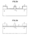
- Ti and Au are vapor deposited all over the surface of the substrate in order to form the hot electrode (1) and the ground electrode (2) by electroplating in the shape of thick films.
- Ti is not shown in the figure, it is used as glue for heightening the adhesive force of the Au electrode.
- the hot electrode (1) and the ground electrode (2) in the form of a thick film having a thickness of 15 ⁇ m are formed on the substrate covered with the vapor deposited Ti and Au.
- excess Ti and Au are removed by dry etching or chemical etching.
- the antistatic film (5) arranged between the hot electrode (1) and the ground electrode (2) comes into contact only with the hot electrode (1) and is not in contact with the ground electrode (2). Accordingly, even when the electric conductivity of the antistatic film (5) fluctuates, the resistance between the electrodes of the modulator can stay unchanged, thereby not affecting the electrical properties of the modulator.
- Fig. 2 there is illustrated a structure of the optical waveguide device according to another embodiment of the present invention.
- This device is a waveguide-type optical intensity modulator (Mach-Zehnder type) and can be produced in the same manner as explained in the case of the optical phase modulator.
- the intensity modulator of this type two Y-branched waveguides are combined such that the lightwave is modulated through branching, phase modulation and combined interference.
- any substrate can be used in the present invention as long as it has an electrooptical effect, and it is evident that the present invention does not rely on the method for forming the waveguide or the crystal orientation of the substrate.
- the present invention is applicable to polarization scramblers and the like.
- an optical waveguide device wherein fluctuations in electrical modulation characteristics of the device are effectively suppressed, thereby realizing excellent temperature properties and suppressed reduction in electric field by applied microwave.
Landscapes
- Physics & Mathematics (AREA)
- Nonlinear Science (AREA)
- Electromagnetism (AREA)
- Chemical & Material Sciences (AREA)
- Engineering & Computer Science (AREA)
- Ceramic Engineering (AREA)
- Crystallography & Structural Chemistry (AREA)
- General Physics & Mathematics (AREA)
- Optics & Photonics (AREA)
- Optical Modulation, Optical Deflection, Nonlinear Optics, Optical Demodulation, Optical Logic Elements (AREA)
- Optical Integrated Circuits (AREA)
Claims (6)
- Optische Wellenleitereinrichtung, umfassend ein Substrat (6) mit einem elektrooptischen Effekt und, gebildet auf einer Oberfläche des Substrats (6), einen optischen Wellenleiter (3) zum Führen einer Lichtwelle, wenigstens ein Paar von Elektroden, die aus einer energieführenden Elektrode (1) und einer Masseelektrode (2) gebildet sind, die eine geführte Lichtwelle steuern, eine Pufferschicht (4), die zwischen den Elektroden und dem optischen Wellenleiter gebildet ist, und ferner umfassend einen antistatischen Film (5), der auf einer oberen Oberfläche der Pufferschicht derart gebildet ist, dass er nur im Kontakt mit der energieführenden Elektrode kommt, dadurch gekennzeichnet, dass ein Spalt (g) zwischen dem antistatischen Film (5) und der Masseelektrode (2) so gewählt wird, dass es möglich ist, eine Verschiebung eines Arbeitspunkts als Folge der thermischen Spannung der optischen Wellenleitereinrichtung mit einer Verschiebung des Arbeitspunkts als Folge einer elektrischen Ladung, die in einem Bereich des Substrats (6) hervorgerufen wird, der direkt unter dem Spalt (6) ist, zu kompensieren.
- Optische Wellenleitereinrichtung nach Anspruch 1, dadurch gekennzeichnet, dass das Substrat (6), auf dem der optische Wellenleiter (3) gebildet ist, aus Lithium-niobat gebildet ist und der optische Wellenleiter durch Bewirken einer thermischen Diffusion von Titan (Ti) gebildet ist.
- Optische Wellenleitereinrichtung nach Anspruch 1 oder 2, dadurch gekennzeichnet, dass der antistatische Film (5), der in Kontakt mit der energieführenden Elektrode (1) ist, aus einem halbleitenden Material gebildet ist
- Optische Wellenleitereinrichtung nach Anspruch 1 oder 2, dadurch gekennzeichnet, dass der antistatische Film (5) aus einem Material gebildet ist, das aus der Gruppe gewählt ist, die aus Ga, In, As, Al, B, Ge, Si, Sn und Sb oder einer Verbindung davon besteht.
- Optische Wellenleitereinrichtung nach irgendeinem der Ansprüche 1 bis 4, dadurch gekennzeichnet, dass der Spalt (g) zwischen dem antistatischen Film (5) und der Masseelektrode (2) als ein derartiger Wert gesetzt ist, der größer als null und kleiner als ein Abstand (S) zwischen den Elektroden (1, 2) ist.
- Optische Wellenleitereinrichtung nach irgendeinem der Ansprüche 1 bis 5, dadurch gekennzeichnet, dass die optische Wellenleitereinrichtung ein Intensitätsmodulator oder ein Phasenmodulator oder ein Polarisations-Scrambler ist.
Applications Claiming Priority (3)
| Application Number | Priority Date | Filing Date | Title |
|---|---|---|---|
| JP154029/96 | 1996-06-14 | ||
| JP8154029A JP2873203B2 (ja) | 1996-06-14 | 1996-06-14 | 導波路型光デバイス |
| JP15402996 | 1996-06-14 |
Publications (2)
| Publication Number | Publication Date |
|---|---|
| EP0813093A1 EP0813093A1 (de) | 1997-12-17 |
| EP0813093B1 true EP0813093B1 (de) | 2004-10-20 |
Family
ID=15575360
Family Applications (1)
| Application Number | Title | Priority Date | Filing Date |
|---|---|---|---|
| EP97304044A Expired - Lifetime EP0813093B1 (de) | 1996-06-14 | 1997-06-10 | Optische Wellenleitervorrichtung |
Country Status (5)
| Country | Link |
|---|---|
| US (1) | US5982958A (de) |
| EP (1) | EP0813093B1 (de) |
| JP (1) | JP2873203B2 (de) |
| CA (1) | CA2207712C (de) |
| DE (1) | DE69731254T2 (de) |
Families Citing this family (14)
| Publication number | Priority date | Publication date | Assignee | Title |
|---|---|---|---|---|
| US6198855B1 (en) * | 1996-07-19 | 2001-03-06 | Jds Uniphase Corporation | Velocity-matched, traveling-wave electro-optical devices using non-conductive and conductive polymer buffer layers |
| US6584239B1 (en) | 1998-05-22 | 2003-06-24 | Bookham Technology Plc | Electro optic modulator |
| JP4471520B2 (ja) * | 2000-09-22 | 2010-06-02 | 日本碍子株式会社 | 進行波形光変調器 |
| WO2002097521A1 (fr) | 2001-05-25 | 2002-12-05 | Anritsu Corporation | Dispositif de modulation optique presentant d'excellentes caracteristiques electriques grace a une restriction efficace du transfert de chaleur |
| US7408693B2 (en) | 2004-07-27 | 2008-08-05 | Jds Uniphase Corporation | Electro-optic device |
| JP2007322599A (ja) | 2006-05-31 | 2007-12-13 | Fujitsu Ltd | 光デバイス |
| US7529433B2 (en) | 2007-01-12 | 2009-05-05 | Jds Uniphase Corporation | Humidity tolerant electro-optic device |
| JP5056040B2 (ja) * | 2007-02-08 | 2012-10-24 | 富士通株式会社 | 光変調器 |
| JP5418222B2 (ja) | 2007-03-27 | 2014-02-19 | 富士通株式会社 | 光デバイス |
| JP2009145816A (ja) * | 2007-12-18 | 2009-07-02 | Ngk Insulators Ltd | 光変調器 |
| US8173045B2 (en) | 2008-05-28 | 2012-05-08 | University Of Washington | Diels-Alder crosslinkable dendritic nonlinear optic chromophores and polymer composites |
| JP2013037243A (ja) * | 2011-08-09 | 2013-02-21 | Fujitsu Optical Components Ltd | 光変調器 |
| JP6578995B2 (ja) * | 2016-03-07 | 2019-09-25 | 住友大阪セメント株式会社 | 導波路型光素子 |
| KR102802802B1 (ko) * | 2023-12-20 | 2025-04-30 | (재)한국나노기술원 | 하이브리드 전광 광변조기 제조방법 및 그 하이브리드 전광 광변조기 그리고 이를 이용한 광신호 위상제어방법 |
Family Cites Families (25)
| Publication number | Priority date | Publication date | Assignee | Title |
|---|---|---|---|---|
| JPS6273207A (ja) * | 1985-09-27 | 1987-04-03 | Fujitsu Ltd | 導波路光デイバイス |
| NL8600782A (nl) * | 1986-03-26 | 1987-10-16 | Nederlanden Staat | Elektro-optisch geinduceerde optische golfgeleider, en actieve inrichtingen waarvan zulk een golfgeleider deel uitmaakt. |
| SE457253B (sv) * | 1987-04-14 | 1988-12-12 | Ericsson Telefon Ab L M | Elektrodanordning foer optoelektroniska organ |
| JPS6457207A (en) * | 1987-08-28 | 1989-03-03 | Hitachi Ltd | Waveguide type optical device |
| US5015053A (en) * | 1989-04-25 | 1991-05-14 | Massachusetts Institute Of Technology | Reduction of modulator non-linearities with independent bias angle control |
| US5061030A (en) * | 1989-08-15 | 1991-10-29 | Optical Measurement Technology Development Co., Ltd. | Optical integrated modulator |
| JP2867560B2 (ja) * | 1990-03-02 | 1999-03-08 | 富士通株式会社 | 光導波路デバイス |
| US5050948A (en) * | 1990-08-23 | 1991-09-24 | Tektronix, Inc. | Traveling wave electro-optic modulator |
| JPH04110831A (ja) * | 1990-08-31 | 1992-04-13 | Nec Corp | 光制御デバイス |
| US5185823A (en) * | 1990-12-13 | 1993-02-09 | Japan Aviation Electronics Industry Limited | Waveguide type optical device |
| FR2672398B1 (fr) * | 1991-02-01 | 1993-11-19 | Alcatel Nv | Dispositif electro-optique a guide d'onde. |
| JPH0561009A (ja) * | 1991-09-04 | 1993-03-12 | Hikari Keisoku Gijutsu Kaihatsu Kk | 光導波路素子 |
| JPH0811664B2 (ja) * | 1991-09-18 | 1996-02-07 | 村田機械株式会社 | 解舒補助装置の制御方法 |
| JPH0588125A (ja) * | 1991-09-26 | 1993-04-09 | Sumitomo Cement Co Ltd | 光導波路及びその作製方法 |
| DE69226761T2 (de) * | 1991-12-27 | 1999-01-14 | Fujitsu Ltd., Kawasaki, Kanagawa | Optische Wellenleiteranordnung mit reduzierter DC-Drift |
| JP2981334B2 (ja) * | 1992-02-17 | 1999-11-22 | 住友大阪セメント株式会社 | 電荷分散用導電膜の形成方法 |
| US5291565A (en) * | 1992-06-30 | 1994-03-01 | Hughes Aircraft Company | Broad band, low power electro-optic modulator apparatus and method with segmented electrodes |
| SE500991C2 (sv) * | 1992-08-17 | 1994-10-17 | Ericsson Telefon Ab L M | Anordning för anpassning av hastigheten för optiska och elektriska signaler i en vågutbredningsstruktur samt dess användning i fiberoptiska system |
| US5621839A (en) * | 1993-08-26 | 1997-04-15 | Ngk Insulators, Ltd. | Optical waveguide device having substrate made of ferroelectric crystals |
| JP2555942B2 (ja) * | 1993-08-27 | 1996-11-20 | 日本電気株式会社 | 光制御デバイス |
| JP3628342B2 (ja) * | 1993-09-17 | 2005-03-09 | 富士通株式会社 | 誘電体光導波路デバイス |
| CA2133300C (en) * | 1993-11-01 | 1999-04-27 | Hirotoshi Nagata | Optical waveguide device |
| JP3231190B2 (ja) * | 1994-08-09 | 2001-11-19 | 住友大阪セメント株式会社 | 導波路型光素子 |
| JP2894961B2 (ja) * | 1994-11-18 | 1999-05-24 | 日本電気株式会社 | 光制御デバイス |
| JPH09269469A (ja) * | 1996-03-29 | 1997-10-14 | Kyocera Corp | 光導波路デバイス |
-
1996
- 1996-06-14 JP JP8154029A patent/JP2873203B2/ja not_active Expired - Fee Related
-
1997
- 1997-05-30 US US08/865,683 patent/US5982958A/en not_active Expired - Lifetime
- 1997-06-10 EP EP97304044A patent/EP0813093B1/de not_active Expired - Lifetime
- 1997-06-10 DE DE69731254T patent/DE69731254T2/de not_active Expired - Fee Related
- 1997-06-13 CA CA002207712A patent/CA2207712C/en not_active Expired - Fee Related
Also Published As
| Publication number | Publication date |
|---|---|
| CA2207712A1 (en) | 1997-12-14 |
| EP0813093A1 (de) | 1997-12-17 |
| US5982958A (en) | 1999-11-09 |
| DE69731254D1 (de) | 2004-11-25 |
| DE69731254T2 (de) | 2005-10-13 |
| CA2207712C (en) | 2005-05-03 |
| JPH103064A (ja) | 1998-01-06 |
| JP2873203B2 (ja) | 1999-03-24 |
Similar Documents
| Publication | Publication Date | Title |
|---|---|---|
| EP0813093B1 (de) | Optische Wellenleitervorrichtung | |
| US7088875B2 (en) | Optical modulator | |
| KR0162755B1 (ko) | 고분자 도파로형 광 세기 변조기 | |
| EP0817988B1 (de) | Polarisationsunabhängiger elektrooptischer modulator | |
| US6721085B2 (en) | Optical modulator and design method therefor | |
| EP2545408B1 (de) | Optische modulatoren mit steuerbarer frequenzmodulation | |
| US20090067770A1 (en) | Lithium niobate optical modulator | |
| EP1020754B1 (de) | Lichtmodulator vom wellenleitertyp | |
| JP2001154164A (ja) | 光変調器および光変調方法 | |
| CA2118272A1 (en) | Electrooptic device structure and method for reducing thermal effects in optical waveguide modulators | |
| US5283842A (en) | Operating point trimming method for optical waveguide modulator and switch | |
| EP0343939B1 (de) | Elektro-optische Vorrichtung | |
| EP2131230A1 (de) | Optische einrichtung | |
| US7088874B2 (en) | Electro-optic devices, including modulators and switches | |
| US7627200B2 (en) | Optical device | |
| US5103491A (en) | Waveguide type optical circuit element | |
| HK1003664A (en) | Optical waveguide device | |
| JPH0816746B2 (ja) | 光導波路素子及びその製造方法 | |
| JPH08160368A (ja) | 半導体光強度変調装置及び半導体光装置 | |
| US5815609A (en) | Waveguide type optical external modulator | |
| JP2800792B2 (ja) | 導波路型偏波スクランブラ | |
| JP2848455B2 (ja) | 導波型光デバイス | |
| JPH06281897A (ja) | 光強度変調器 | |
| JP2814967B2 (ja) | 導波路型光デバイス | |
| JP2606552B2 (ja) | 光制御デバイス |
Legal Events
| Date | Code | Title | Description |
|---|---|---|---|
| PUAI | Public reference made under article 153(3) epc to a published international application that has entered the european phase |
Free format text: ORIGINAL CODE: 0009012 |
|
| AK | Designated contracting states |
Kind code of ref document: A1 Designated state(s): DE FR GB IT |
|
| 17P | Request for examination filed |
Effective date: 19971128 |
|
| AKX | Designation fees paid |
Free format text: DE FR GB IT |
|
| RBV | Designated contracting states (corrected) |
Designated state(s): DE FR GB IT |
|
| 17Q | First examination report despatched |
Effective date: 20030626 |
|
| GRAP | Despatch of communication of intention to grant a patent |
Free format text: ORIGINAL CODE: EPIDOSNIGR1 |
|
| GRAS | Grant fee paid |
Free format text: ORIGINAL CODE: EPIDOSNIGR3 |
|
| GRAA | (expected) grant |
Free format text: ORIGINAL CODE: 0009210 |
|
| AK | Designated contracting states |
Kind code of ref document: B1 Designated state(s): DE FR GB IT |
|
| REG | Reference to a national code |
Ref country code: GB Ref legal event code: FG4D |
|
| REF | Corresponds to: |
Ref document number: 69731254 Country of ref document: DE Date of ref document: 20041125 Kind code of ref document: P |
|
| REG | Reference to a national code |
Ref country code: HK Ref legal event code: WD Ref document number: 1003664 Country of ref document: HK |
|
| PLBE | No opposition filed within time limit |
Free format text: ORIGINAL CODE: 0009261 |
|
| STAA | Information on the status of an ep patent application or granted ep patent |
Free format text: STATUS: NO OPPOSITION FILED WITHIN TIME LIMIT |
|
| ET | Fr: translation filed | ||
| 26N | No opposition filed |
Effective date: 20050721 |
|
| PGFP | Annual fee paid to national office [announced via postgrant information from national office to epo] |
Ref country code: IT Payment date: 20090617 Year of fee payment: 13 |
|
| PGFP | Annual fee paid to national office [announced via postgrant information from national office to epo] |
Ref country code: GB Payment date: 20090610 Year of fee payment: 13 Ref country code: DE Payment date: 20090604 Year of fee payment: 13 |
|
| GBPC | Gb: european patent ceased through non-payment of renewal fee |
Effective date: 20100610 |
|
| REG | Reference to a national code |
Ref country code: FR Ref legal event code: ST Effective date: 20110228 |
|
| PG25 | Lapsed in a contracting state [announced via postgrant information from national office to epo] |
Ref country code: IT Free format text: LAPSE BECAUSE OF NON-PAYMENT OF DUE FEES Effective date: 20100610 |
|
| PG25 | Lapsed in a contracting state [announced via postgrant information from national office to epo] |
Ref country code: DE Free format text: LAPSE BECAUSE OF NON-PAYMENT OF DUE FEES Effective date: 20110101 |
|
| PG25 | Lapsed in a contracting state [announced via postgrant information from national office to epo] |
Ref country code: FR Free format text: LAPSE BECAUSE OF NON-PAYMENT OF DUE FEES Effective date: 20100630 |
|
| PG25 | Lapsed in a contracting state [announced via postgrant information from national office to epo] |
Ref country code: GB Free format text: LAPSE BECAUSE OF NON-PAYMENT OF DUE FEES Effective date: 20100610 |
|
| PGFP | Annual fee paid to national office [announced via postgrant information from national office to epo] |
Ref country code: FR Payment date: 20090611 Year of fee payment: 13 |