EP0813292A2 - Onduleur de puissance avec au moins trois unités onduleur de puissance commandées en parallèle par modulation de largeur d'impulsion - Google Patents
Onduleur de puissance avec au moins trois unités onduleur de puissance commandées en parallèle par modulation de largeur d'impulsion Download PDFInfo
- Publication number
- EP0813292A2 EP0813292A2 EP97109484A EP97109484A EP0813292A2 EP 0813292 A2 EP0813292 A2 EP 0813292A2 EP 97109484 A EP97109484 A EP 97109484A EP 97109484 A EP97109484 A EP 97109484A EP 0813292 A2 EP0813292 A2 EP 0813292A2
- Authority
- EP
- European Patent Office
- Prior art keywords
- pwm
- phase
- inverting units
- juxtaposed
- type
- Prior art date
- Legal status (The legal status is an assumption and is not a legal conclusion. Google has not performed a legal analysis and makes no representation as to the accuracy of the status listed.)
- Withdrawn
Links
Images




Classifications
-
- H—ELECTRICITY
- H02—GENERATION; CONVERSION OR DISTRIBUTION OF ELECTRIC POWER
- H02M—APPARATUS FOR CONVERSION BETWEEN AC AND AC, BETWEEN AC AND DC, OR BETWEEN DC AND DC, AND FOR USE WITH MAINS OR SIMILAR POWER SUPPLY SYSTEMS; CONVERSION OF DC OR AC INPUT POWER INTO SURGE OUTPUT POWER; CONTROL OR REGULATION THEREOF
- H02M7/00—Conversion of AC power input into DC power output; Conversion of DC power input into AC power output
- H02M7/42—Conversion of DC power input into AC power output without possibility of reversal
- H02M7/44—Conversion of DC power input into AC power output without possibility of reversal by static converters
- H02M7/48—Conversion of DC power input into AC power output without possibility of reversal by static converters using discharge tubes with control electrode or semiconductor devices with control electrode
- H02M7/505—Conversion of DC power input into AC power output without possibility of reversal by static converters using discharge tubes with control electrode or semiconductor devices with control electrode using devices of a thyratron or thyristor type requiring extinguishing means
- H02M7/515—Conversion of DC power input into AC power output without possibility of reversal by static converters using discharge tubes with control electrode or semiconductor devices with control electrode using devices of a thyratron or thyristor type requiring extinguishing means using semiconductor devices only
- H02M7/525—Conversion of DC power input into AC power output without possibility of reversal by static converters using discharge tubes with control electrode or semiconductor devices with control electrode using devices of a thyratron or thyristor type requiring extinguishing means using semiconductor devices only with automatic control of output waveform or frequency
- H02M7/527—Conversion of DC power input into AC power output without possibility of reversal by static converters using discharge tubes with control electrode or semiconductor devices with control electrode using devices of a thyratron or thyristor type requiring extinguishing means using semiconductor devices only with automatic control of output waveform or frequency by pulse width modulation
-
- H—ELECTRICITY
- H02—GENERATION; CONVERSION OR DISTRIBUTION OF ELECTRIC POWER
- H02M—APPARATUS FOR CONVERSION BETWEEN AC AND AC, BETWEEN AC AND DC, OR BETWEEN DC AND DC, AND FOR USE WITH MAINS OR SIMILAR POWER SUPPLY SYSTEMS; CONVERSION OF DC OR AC INPUT POWER INTO SURGE OUTPUT POWER; CONTROL OR REGULATION THEREOF
- H02M7/00—Conversion of AC power input into DC power output; Conversion of DC power input into AC power output
- H02M7/42—Conversion of DC power input into AC power output without possibility of reversal
- H02M7/44—Conversion of DC power input into AC power output without possibility of reversal by static converters
- H02M7/48—Conversion of DC power input into AC power output without possibility of reversal by static converters using discharge tubes with control electrode or semiconductor devices with control electrode
- H02M7/493—Conversion of DC power input into AC power output without possibility of reversal by static converters using discharge tubes with control electrode or semiconductor devices with control electrode the static converters being arranged for operation in parallel
-
- H—ELECTRICITY
- H02—GENERATION; CONVERSION OR DISTRIBUTION OF ELECTRIC POWER
- H02M—APPARATUS FOR CONVERSION BETWEEN AC AND AC, BETWEEN AC AND DC, OR BETWEEN DC AND DC, AND FOR USE WITH MAINS OR SIMILAR POWER SUPPLY SYSTEMS; CONVERSION OF DC OR AC INPUT POWER INTO SURGE OUTPUT POWER; CONTROL OR REGULATION THEREOF
- H02M7/00—Conversion of AC power input into DC power output; Conversion of DC power input into AC power output
- H02M7/42—Conversion of DC power input into AC power output without possibility of reversal
- H02M7/44—Conversion of DC power input into AC power output without possibility of reversal by static converters
- H02M7/48—Conversion of DC power input into AC power output without possibility of reversal by static converters using discharge tubes with control electrode or semiconductor devices with control electrode
Definitions
- the present invention relates to a power inverter having three or more parallel driven PWM-type power inverting units so as to extend an output capacity thereof.
- the present invention more particularly, relates to the power inverter which controls its output voltage according to a switching control method of a, so-called, PWM (Pulse Width Modulation) method using power switching devices such as bipolar transistors or IGBTs (Insulated Gate Bipolar Transistors) in which an output current balance between the respective PWM-type inverting units and in which an output current balance between output currents from the respective PWM-type inverting units is taken.
- PWM Pulse Width Modulation
- a power inverter serves to invert a DC voltage into a corresponding AC voltage by turning on and off the DC voltage using the switching devices in a time division manner.
- a United States Patent No. 5,253,155 issued on October 12, 1993 (which corresponds to a Japanese Patent Application First Publication No. Heisei 5-30661 published on February 5, 1993 and corresponds to a European Patent No. EP 0 524 398 B1 published on August 21, 1996) exemplifies another method of extending the capacity of the power inverter in which two PWM-type inverting units are parallel driven.
- a power inverter comprising:
- a power inverter comprising:
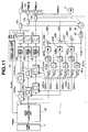
- Fig. 1 is a circuit block diagram of a power inverter in a first preferred embodiment according to the present invention in which three power inverting units are driven in parallel.
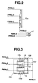
- Fig. 2 is a wiring diagram of a U-phase (representative) integrated interphase reactor shown in Fig. 1.
- Fig. 3 is an explanatory view of a first example of a structure of the U-phase interphase reactor shown in Fig. 2.
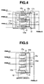
- Fig. 4 is an explanatory view of a second example of the structure of the U-phase interphase reactor shown in Fig. 2.
- Fig. 5 is an explanatory view of a second example of the structure of the U-phase interphase reactor shown in Fig. 2.
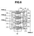
- Fig. 6 is an explanatory view of a third example of the structure of the U-phase interphase reactor shown in Fig. 2.
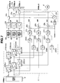
- Fig. 7 is a circuit block diagram of a current balance controller shown in Fig. 1.
- Figs. 8A, 8B, 8C, 8D, and 8E are integrally a timing chart for explaining an operation of the current balance controller shown in Fig. 7.
- Fig. 9 is a circuit block diagram of the current balance controller in a second preferred embodiment of the power inverter according to the present invention.
- Figs. 10A, 10B, 10C, 10D, and 10E are integrally a timing chart for explaining an operation of the current balance controller shown in Fig. 9.
- Fig. 11 is a circuit block diagram of the current balance controller in a third preferred embodiment according to the present invention.
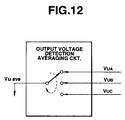
- Fig. 12 is a functional block diagram of a voltage detection and averaging circuit used in each embodiment of the current balance controller.
- Figs. 13A, 13B, 13C, 13D, and 13E are integrally a timing chart for explaining an operation of the voltage detection and averaging circuit shown in Fig. 12.
- Fig. 1 shows a circuit block diagram of a power inverter in a first preferred embodiment according to the present invention.
- the power inverter includes three PWM-type power inverting units parallel driven.
- the present invention is applicable to the power inverter in which four or more PWM-type power inverting units can be driven in parallel.
- a PWM generator 5 in response to an inputted voltage instruction and a frequency instruction, generates and outputs a PWM (Pulse Width Modulation) pulse to each phase line thereof, a period and width being dependent upon the voltage instruction and the frequency instruction.
- PWM Pulse Width Modulation
- a three-phase AC power supply is connected across a power converter 1 which corresponds to the AC power supply into a corresponding DC power supply.
- An electrostatic capacitor is connected across both terminals of the AC-DC converter and both bias terminals of three-phase three PWM-type power inverting units 2A, 2B, and 2C is connected in parallel to each other across the electrostatic capacitor.
- Each PWM-type power inverting unit 2A, 2B, and 2C includes serially connected U-phase transistors, serially connected V-phase transistors, and serially connected W-phase transistors. Each junction of the serially connected transistors is connected as a phase output of each PMW-type power inverting unit 2A, 2B, and 2C via a corresponding one of the three interphase reactors 10u, 10v, and 10w to a load such as a three-phase induction motor 4.
- Each gate (or base) end of the totally eighteen (6 x 3) serially connected transistors in the respective PWM-type power inverting units 2A, 2B, and 2C is connected to a drive circuit having a dead time compensation circuit (dead time ckt.) 6A, 6B, and 6C.
- Each phase output end of each of the PWM-type power inverting units 2A, 2B, and 2C is connected to a corresponding one of current detectors (constituted by, for example, a current transformer) 12u, 12v, 12w, 13u, 13v, 13w, 14u, 14v, and 14w to detect each phase output current of each of the power inverting units 2A, 2B, and 2C.
- phase output currents 1uA, 1vA, 1wA, 1uB, 1vB, 1wB, 1uC, 1vC, and 1wC of each of the three PWM-type power inverting units 2A, 2B, and 2C is inputted to a current balance controller 11.
- Each input end of the integrated interphase reactors 10u, 10v, and 10w having the same instantaneous magnetic polarity indicating dot marks is connected to each corresponding phase output end of the respective PWM-type inverting units 2A, 2B, and 2C.
- Each output end of the integrated interphase reactors 10u, 10v, and 10w is interconnected to the load 4.
- the three-phase current balance controller 11 fetches phase output currents of the respective PWM-type power inverting units IuA, IvA, IwA, IuB, IvB, IwB, IuC, IvC, and IwC thereinto, carries out a current balancing correction for the inputted PWM waveform from the PWM generator 5, and provides the current balance corrected PWM waveform for the respective gate drive circuits 6A, 6B, and 6C.
- FIG. 2 shows a first example of one of the integrated interphase reactors as the U-phase integrated interphase reactor 10u.
- each dot marked input end of each coil in the U-phase integrated interphase reactor 10u is connected to the corresponding U-phase output ends of PWMu-A, PWMv-B, and PWMw-C of the respective three PWM-type power inverting units 2A, 2B, and 2C.
- the respective three coils of the U-phase integrated interphase reactor 10u are magnetically coupled with the iron core and are formed in a star connection whose neutral point serves as a synthesized output end.
- the respective three coils of the respresentative U-phase integrated interphase reactor 10u are magnetically coupled with the iron core and are formed in a star connection whose neutral point serves as a synthesized output end.
- a structure of each interphase reactor is constituted by a magnetic core member made of an iron and having a plurality of juxtaposed leg portions extended integrally from a connection leg portion and the plurality of coils each having the same number of windings and each wound around a corresponding one of the juxtaposed leg portions so as to interlink to the corresponding one of the juxtaposed leg portions.
- the number of the coils in each integrated interphase reactor is N (N denotes the number of the parallel driven PWM-type power inverting units).
- Each winding start end of the coils 15u, 15v, and 15w in the U-phase integrated interphase reactor 10u is connected to each U-phase output end PWMu-A, PWMu-B, and PWMu-C of the three power inverting units 2A, 2B, and 2C.
- Each winding end of the respective coils 15u, 15v, and 15w in the U-phase integrated interphase reactor 10u is connected together to a corresponding one PWMu-O of the phase input ends of the induction motor 4.
- the iron core is of a three leg iron core type having a connection leg portion 16A and is provided with another iron core 16B with a gap G against each free end of the juxtaposed leg portions.
- the power inverter in the first embodiment includes the three PWM-type power inverting units 2A, 2B, and 2C parallel connected via the three integrated interphase reactors, one of which is shown in Fig. 3, in order to extend furthermore the capacity of the power inverter. Consequently, the above-described inductance effect can be achieved and can be applied to the power inverter having the two or more power inverting units.
- Fig. 4 shows a second example of the structure of the U-phase integrated interphase reactor 10u.
- the magnetic core member includes three letter U-shaped iron cores (so-called, two-leg iron cores) 17 2 , 17 3 , and 17 4A , small-sized two of the letter U-shaped iron cores 17 2 and 17 3 being juxtaposed to each other and the remaining letter U-shaped iron core 17 4A being arranged so as to enclose the small-sized juxtaposed two U-shaped iron cores 17 2 and 17 3 .
- One of the three coils 15u, 15v, and 15w which is for the U-phase output end PWMu-A of a first of the three power inverting units 2A is wound on the juxtaposed leg portions of the remaining letter U-shaped iron core 17 4A and one of the two letter U-shaped iron cores 17 2 .
- One of the three coils 15u, 15v, and 15w which is for the U-phase output end PWMu-B of a second of the three power inverting units 2B is wound on the juxtaposed leg portions of the two small-sized letter U-shaped iron cores 17 2 and 17 3 .
- the remaining one of the three coils 15u, 15v, and 15w which is for the U-phase output end PWMu-C of a third of the three power inverting units 2C is wound on the remaining juxtaposed leg portion of the remaining large-sized U-shaped iron core and the remaining juxtaposed leg portion of the small-sized U-shaped iron core 17 3 .
- Three other iron cores 17 1 are faced against free ends of the respective three letter U-shaped iron cores 172, 173, and 174 with the same distances of the gaps.
- connection of the winding ends of the respective coils 15u, 15v, and 15w are the same as those shown in Fig. 8.
- the same structure as shown in Fig. 4 applies equally well to the V-phase and W-phase integrated interphase reactors 10v and 10w.
- Fig. 5 shows a third example of the structure of the U-phase integrated interphase reactor 10u.
- the number of the juxtaposed leg portions of the integrated iron core 16A is increased by one as compared with Fig. 3 (N + 1).
- a short-circuited coil 18 is wound in the same direction as each of the three coils 15u, 15v, and 15w on the newly added leg portion of the iron core 16A.
- the other iron core 16B is faced against a free end of the newly added leg portion of the iron core 16A.
- the short-circuited coil 18 acts to suppress the variation in the interlinkage magnetic fluxes around the three coils 15u, 15v, and 15w and operates in response to a transient variation in the magnetic fluxes as if an extra leg on which the short-circuit coil 18 is wound were not present.
- Fig. 6 shows a fourth example of the structure of the U-phase integrated interphase reactor 10u.
- the short-circuited coil 18 is wound on the remaining juxtaposed leg portions of one 17 3 of the small-sized U-shaped iron core 17 1 .
- the small-sized U-shaped iron cores are three 17 2 , 17 3 , and 17 4 in the case of Fig. 6.
- the other structure is generally the same as that shown in Fig. 4.
- Fig. 7 shows the detailed circuit block diagram of the current balance controller 11 in the first embodiment shown in Fig. 1, particularly describing the U-phase current balance controller.
- the above-described three integrated interphase reactors 10u, 10v, and 10w are utilized to constitute the parallel connected three PWM-type power inverting units 2A, 2B, and 2C.
- each integrated interphase reactor 10u, 10v, and 10w can suppress the variation in the transverse currents generated due to the variations in the magnetic fluxes generated due to the difference in magnitudes of the corresponding phase output currents, each integrated interphase reactor 10u, 10v, and 10w cannot suppress those in DC components.
- Fig. 7 shows the U-phase related power inverting units 2A, 2B, and 2C and the U-phase related current balance controller 11.
- a rise time of each PWM pulse PWMu* derived from the PWM generator 5 is delayed by means of each rise time corrector 20Aup, 20Bup, and 20Cup for the corresponding one of the power inverting units 2A, 2B, and 2C.
- a fall time of each PWM pulse PWMu* derived from the PWM generator 5 is delayed by means of each fall time corrector 21Adown, 21Bdown, and 21Cdown.
- Each delay time set by the corresponding one of the rise time correctors 20Aup, 20Bup, and 20Cup is controlled by a corresponding one of respective positive polarity amplifiers 22Ap, 22Bp, and 22Cp.
- each delay time set by the corresponding one of the respective fall time correctors 21Adown, 21Bdown, and 21Cdown is controlled by a corresponding one of respective negative polarity amplifiers 23AN, 23BN, and 23CN.
- Input signals of these amplifiers 22Ap, 22Bp, 22Cp, 23BN, and 23CN are derived according to the deviation between each one of the detected U-phase output currents IAU, IBU, and ICU and the average U-phase current Iuave and the polarity of the deviation (namely, whether the result of the subtraction indicates positive or negative).
- Each deviation calculator 26A, 26B, and 26C serves to derive a deviation between each U-phase output current IAU, IBU, and ICU and the average U-phase current Iuave and its polarity (plus or minus).
- Each deviation control amplifier 27A, 27B, and 27C calculates a proportional-integration (P-I) using a proportional coefficient (correction gain) Kp from the corresponding one of the deviation calculators 26A, 26B, and 26C.
- P-I proportional-integration
- Kp proportional coefficient
- the result of the P-I calculation of each deviation control amplifier 27A, 27B, and 27C is inputted into the corresponding two of the respective polarity amplifiers 22Ap, 22Bp, 22Cp and 23AN, 23BN, and 23CN.
- the corresponding PWM pulse PWMu* in the corresponding one of the rise time correctors 20Aup, 20Bup, and 20Cup is delayed according to the deviation via the corresponding one of the positive polarity amplifiers 22Ap, 22Bp, and 22Cp.
- the corresponding PWM pulse OPWMu* in the corresponding one of the fall time correctors 21Adown, 21Bdown, and 21Cdown is delayed accoring to the deviation via the corresponding one of the negative polarity amplifiers 23AN, 23BN, and 23CN.
- Figs. 8A, 8B, 8C, 8D, and 8E integrally show a signal timing chart of each signal at parts of the power inverter shown in Figs. 1 and 7.
- the PWM instruction shown in Fig. 8A corresponds to PWMu* shown in Fig. 7.
- the PWMu-A, PWMu-B, and PWMu-C shown in Figs. 8B, 8C, and 8D corresponds to those respective U-phase output signals from the respective power inverting units 2A, 2B, and 2C shown in Figs. 1 and 7.
- the synthesized output voltage shown in Fig. 8E corresponds to PWMu-O shown in Fig. 7.
- Portions in Fig. 8B denoted by oblique lines corresponds to time domains in which the current balance controller 11 carries out the current balance controller 11 carries out the current balance corrections for the PWMu-A pulse, for the PWMu-B pulse , and for the PWMu-C pulse, respectively.
- each leading edge of the PWMu-A and PWMu-C pulse for the first and third power inverting units 2A and 2C is delayed and each trailing edge of the PWMu-B pulse for the second power inverting unit 2B is delayed.
- These corrective controls can achieve the current balance by retarding the rise time or the fall time of each PWM waveform of the same phases which is unbalanced in the output currents in the same phases of the respective three power inverting units 2A, 2B, and 2C.
- the rise time and/or the fall time of any one, any two, or all of the output PWMu, PWMv, and PWMw pulses of the respective three power inverting units 2A, 2B, and 2C is delayed during and according to the development in the corresponding current unbalanced state.
- a switching delay timing of the output voltage derived from each of the power inverting units and synthesized by each corresponding integrated interphase reactor is 10u, 10v, and 10w is varied according to a current unbalanced quantity.
- Fig. 9 shows a second preferred embodiment of the power inverter in which the current balance controller 11 is designed to suppress the variation of the above-described switching delay timing.
- a constant delay time duration Tbo is added to each set delay time in each corresponding one of the rise time and fall time correctors 20Aup, 20Bup, 20Cup, 21Adown, 21Bdown, and 21Cdown and the positive and negative values of the respective delay times derived according to the deviation between each pulse current output of the corresponding one of the power inverting units 2A, 2B, and 2C and its average current value are added to the constant delay time deviation Tbo.
- the above-described function of the current balance controller 11 corresponds to limiters 30ApL, 30BpL, and 30CpL, 31ANL, 31BNL, and 31CNL and adders 32ApA, 32BpA, 32CpA, and 33ANA, 33BNA, and 33CAN as shown in Fig. 9.
- Each limiter 30ApL, 30BpL, and 30CpL has a positive limit value and a negative limit value, above of both limit values of which the delay control signal from the corresponding one of the deviation control amplifiers 27 A , 27 B , and 27 C is limited to provide a corresponding limited delay control signal.
- the limited delay control signal passed through the corresponding one of the limiters 30ApL, 30BpL, and 30CpL is added to an offset signal corresponding to the constant delay time duration Tbo by means of the corresponding one of the adders 33ApA, 33BpA, and 33CpA to provide the delay control signal. Consequently, the delay correction signal is supplied to the corresponding one of the rise time correctors 20Aup, 20Bup, and 20Cup.
- Each limiter 31ANL, 31BNL, and 31CNL has negative limit value and the positive limit value as reversed from each limiter 30ApL, 30BpL, and 30CpL, above of both limit values of which the delay control signal from the corresponding one of the deviation control amplifiers 27A, 27B, and 27C is limited to provide the corresponding delay control signal having the polarity opposite to the corresponding delay control signal derived from the corresponding one of the limiters 30ApL, 30BpL, and 30CpL.
- the delay control signal derived from the corresponding one of the limiters 27A, 27B, and 27C is added to the offset signal corresponding to the constant time duration Tbo by means of the corresponding one of the adders 33ANA, 33BNA, and 33CAN to provide the delay correction signal.
- the delay correction signal derived from the corresponding one of the adders 33ANA, 33BNA, and 33CAN is supplied to the corresponding one of the fall time correctors 21Adown, 21Bdown, and 21Cdown.
- Figs. 10 A, 10B, 10C, 10D, and 10E integrally show the signal timing chart in the power inverter in the case of the second embodiment shown in Fig. 9.
- Each of the oblique lines shown in Fig. 10B, Fig. 10C, and Fig. 10D denotes the time domain in which the delay time set in the corresponding one of the rise time and fall time correctors 20Aup to 21Cdown from which or to which the constant delay time duration Tbo is subtracted or added.
- each leading edge of the corresponding PWM waveforms PWMu-A and PWMu-B of the first and third power inverting units 2A and 2C are delayed with the control time duration Tbo added and each trailing edge of the corresponding PWM waveforms PWMu-A and PWMu-C of the first and third power inverting units 2A and 2C is delayed with the constant time duration Tbo added in the opposite direction.
- the trailing edge of the PWM pulse waveform PWMu-B of the second power inverting unit 2B is delayed by the time corresponding to the offset signal of the constant time duration Tbo and the leading edge thereof is delayed by the delayed time substracted from the offset signal of the constant delay time duration Tbo.
- the dead time compensation circuit provided in each of the gate drive circuits 6A, 6B, and 6C serves to derive a dead time compensated PWM waveform output by comparing the PWM waveform output by comparing the PWM waveform delayed by means of the current balance controller 11 shown in Fig. 7 or Fig. 9 as a reference with a corresponding output voltage phase of the respective three power inverting units 2A, 2B, and 2C. It is noted that variations in switching times of the respective switching devices (power transistors) in the respective power inverting units 2A, 2B, and 2C can be compensated for by the dead time compensation circuits provided in the respective gate circuits 6A, 6B, and 6C.
- Fig. 11 shows a third preferred embodiment of the power inverter in which a detection of voltage used to compensate for the dead time and for the switching time variation described above is achieved with the current balance controller 11 used for the N (N ⁇ 3) parallel driven power inverting units.
- the individual dead time compensation circuits provided in the respective gate drive circuits 6A, 6B, and 6C are moved as a single (U-phase purpose) dead time compensation circuit 35 installed at a preceding stage to the current balance controller 11 and a compensation value of the dead time compensation circuit 35 is derived from an output voltage averaging circuit 36.
- the output voltage averaging curcuit 36 sequentially fetches each of the output voltage VuA, VuB, and VuC of the respective U-phase sided power inverting units 2A, 2B, and 2C thereinto for each period of a basic clock installed in the current balance controller 11 in a time division manner and derives an average value Vuave of these fetched output voltages VuA, VuB, and VuC, as typically shown in Fig. 12.
- Figs. 13A, 13B, 13C, and 13D integrally show an operation timing chart of the output voltage averaging circuit 36.
- Fig. 13A shows a selection signal based on the basic clock.
- the time division processing permits the derivation of the averaged output voltage equivalent to the average output voltage of each power inverting unit 2A, 2B, and 2C even if the output voltage waveforms of the respective power inverting units 2A, 2B, and 2C are different from each other.
- Figs. 7 through 13 show only the U-phase related circuitry, the same circuit structure is applied to the V-phase and W-phase related circuitry.
- PWMu* is changed to PWMv* and PWMw*, IUA to IVA and IWA, IUB to IVB and IWB, IUC to IVC and IWC, Iuave to Ivave and Iwave, PWMu-A to PWMv-A and PWMw-A, PWMu-B to PWMv-B and PWMv-C, PWMu-C to PWMv-C and PWMw-C, 12u to 12v and 12w, 13u to 13v and 13w, 14u to 14v and 14w, PWMu-0 to PWMv-0 and PWMw-0, and Vuave to Vvave and Vwave.
- the number of turns of the short-circuited coil 18 may be arbitrary but the winding direction of the short-circuited coil 18 is the same as that of each of the other coils.
Landscapes
- Engineering & Computer Science (AREA)
- Power Engineering (AREA)
- Inverter Devices (AREA)
- Supply And Distribution Of Alternating Current (AREA)
Applications Claiming Priority (2)
| Application Number | Priority Date | Filing Date | Title |
|---|---|---|---|
| JP8150529A JPH09331682A (ja) | 1996-06-12 | 1996-06-12 | 電力変換器 |
| JP150529/96 | 1996-06-12 |
Publications (2)
| Publication Number | Publication Date |
|---|---|
| EP0813292A2 true EP0813292A2 (fr) | 1997-12-17 |
| EP0813292A3 EP0813292A3 (fr) | 1999-05-19 |
Family
ID=15498873
Family Applications (1)
| Application Number | Title | Priority Date | Filing Date |
|---|---|---|---|
| EP97109484A Withdrawn EP0813292A3 (fr) | 1996-06-12 | 1997-06-11 | Onduleur de puissance avec au moins trois unités onduleur de puissance commandées en parallèle par modulation de largeur d'impulsion |
Country Status (5)
| Country | Link |
|---|---|
| US (1) | US5852554A (fr) |
| EP (1) | EP0813292A3 (fr) |
| JP (1) | JPH09331682A (fr) |
| KR (1) | KR100276545B1 (fr) |
| CN (1) | CN1067188C (fr) |
Cited By (6)
| Publication number | Priority date | Publication date | Assignee | Title |
|---|---|---|---|---|
| CN100337379C (zh) * | 2005-11-17 | 2007-09-12 | 上海思源电气股份有限公司 | 基于磁控电抗器的电压无功综合控制装置 |
| AT502269B1 (de) * | 2000-08-28 | 2008-12-15 | Thomas M Wolbank | Verfahren zur erkennung von asymmetrien in umrichtergespeisten drehfeldmaschinen während des betriebes durch auswertung von transienten stromänderungen |
| DE102007063434A1 (de) | 2007-06-29 | 2009-01-02 | Enasys Gmbh | Wechselrichtersystem und Steuerverfahren |
| EP2980975A1 (fr) * | 2014-08-01 | 2016-02-03 | General Electric Company | Systèmes et procédés de diagnostics avancés dans des convertisseurs de puissance modulaire |
| EP2725701B1 (fr) | 2012-09-14 | 2021-09-01 | General Electric Company | Commande d'équilibrage de courant dans un convertisseur pour système de turbine éolienne avec générateur d'induction à alimentation double |
| EP4429099A1 (fr) * | 2023-03-10 | 2024-09-11 | Abb Schweiz Ag | Agencement pour le partage de courant d'onduleurs connectés en parallèle |
Families Citing this family (45)
| Publication number | Priority date | Publication date | Assignee | Title |
|---|---|---|---|---|
| GB2330254B (en) | 1997-10-09 | 2000-10-18 | Toshiba Kk | Multiple inverter system |
| KR100319932B1 (ko) * | 1998-10-07 | 2002-04-22 | 장병우 | 전동기의과전압방지장치 |
| US6111329A (en) | 1999-03-29 | 2000-08-29 | Graham; Gregory S. | Armature for an electromotive device |
| US6377478B1 (en) | 1999-05-28 | 2002-04-23 | Toshiba International Corporation | Inverter device |
| US6731524B2 (en) * | 2001-05-21 | 2004-05-04 | Marconi Communications, Inc. | Parallel connected DC regulators with power factor corrected rectifier inputs |
| CN1170354C (zh) * | 2001-12-25 | 2004-10-06 | 艾默生网络能源有限公司 | 并联逆变器系统 |
| FI113720B (fi) * | 2002-06-13 | 2004-05-31 | Abb Oy | Menetelmä suuntaajasiltojen yhteydessä |
| US6535402B1 (en) * | 2002-07-12 | 2003-03-18 | Delta Electronics Inc. | Adaptive compensation of dead time for inverter and converter |
| US20040071003A1 (en) * | 2002-09-04 | 2004-04-15 | G & G Technology, Inc. | Split phase polyphase inverter |
| JP4112930B2 (ja) * | 2002-09-04 | 2008-07-02 | 東芝三菱電機産業システム株式会社 | インバータ装置 |
| CN1312645C (zh) * | 2002-11-14 | 2007-04-25 | 新巨企业股份有限公司 | 压电式转换驱动装置 |
| JP4581574B2 (ja) * | 2004-09-08 | 2010-11-17 | 株式会社ジェイテクト | モータ制御装置及び電動パワーステアリング装置 |
| JP4742989B2 (ja) * | 2006-05-26 | 2011-08-10 | 株式会社日立製作所 | モータ駆動用半導体装置とそれを有するモータ及びモータ駆動装置並びに空調機 |
| US7692938B2 (en) * | 2006-09-06 | 2010-04-06 | Northern Power Systems, Inc. | Multiphase power converters and multiphase power converting methods |
| GB2449427B (en) * | 2007-05-19 | 2012-09-26 | Converteam Technology Ltd | Control methods for the synchronisation and phase shift of the pulse width modulation (PWM) strategy of power converters |
| WO2009094589A1 (fr) * | 2008-01-24 | 2009-07-30 | Birnbach Curtis A | Onduleur haute tension |
| US8036004B2 (en) * | 2008-10-01 | 2011-10-11 | Toshiba International Corporation | Uninterruptible power supply with total isolation |
| US9059603B2 (en) * | 2008-12-11 | 2015-06-16 | Sunline Jamaica Limited | Solar powered electrical energy generating device |
| DE102009018143A1 (de) * | 2009-04-08 | 2010-10-14 | Aesculap Ag | Chirurgische Motorsteuerungs- und/oder -regelungsvorrichtung, chirurgisches Antriebssystem und Verfahren zum Steuern und/oder Regeln einer chirurgischen Antriebseinheit |
| JP5162703B2 (ja) * | 2009-05-07 | 2013-03-13 | シーメンス アクチエンゲゼルシヤフト | 電力変換装置および電力供給装置 |
| KR20120060271A (ko) * | 2010-12-01 | 2012-06-12 | 한국전기연구원 | 전류 밸런서를 이용한 인버터 병렬운전 풍력발전 시스템 |
| US10757830B1 (en) * | 2011-03-11 | 2020-08-25 | Lex Products Corp | Power management and distribution system and method |
| KR101590211B1 (ko) * | 2011-04-01 | 2016-01-29 | 엘에스산전 주식회사 | 고압 인버터 시스템 |
| JP5745931B2 (ja) * | 2011-05-17 | 2015-07-08 | 本田技研工業株式会社 | インバータ発電機の制御装置 |
| RU2518905C2 (ru) * | 2011-05-17 | 2014-06-10 | Хонда Мотор Ко., Лтд. | Управляющее устройство обеспечения параллельной работы для инверторного генератора |
| RU2515474C2 (ru) * | 2011-05-17 | 2014-05-10 | Хонда Мотор Ко., Лтд. | Инверторный генератор |
| RU2540416C2 (ru) * | 2011-05-17 | 2015-02-10 | Хонда Мотор Ко., Лтд. | Инверторный генератор |
| CN103312187B (zh) * | 2012-03-09 | 2016-02-03 | 台达电子工业股份有限公司 | 一种变流器系统 |
| CN104221271B (zh) * | 2012-03-30 | 2017-10-24 | 东芝三菱电机产业系统株式会社 | 功率转换装置 |
| US10698430B2 (en) | 2012-12-19 | 2020-06-30 | Intel Corporation | Method and apparatus of current balancing for multiple phase power converter |
| CN103475248B (zh) | 2013-08-30 | 2016-12-07 | 华为技术有限公司 | 功率变换电路和功率变换系统 |
| DK178199B1 (en) * | 2013-10-23 | 2015-08-03 | Wind Solutions As Kk | Method for controlling the shape of the rising and falling edges of an output voltage pulse of a PWM converter |
| KR101610469B1 (ko) | 2014-05-15 | 2016-04-07 | 현대자동차주식회사 | 다상 인터리브 컨버터 및 이의 제어 방법 |
| WO2016037623A1 (fr) * | 2014-09-12 | 2016-03-17 | Vestas Wind Systems A/S | Bobine d'arrêt pour commutation entrelacée |
| KR101695546B1 (ko) * | 2015-06-01 | 2017-01-12 | 엘에스산전 주식회사 | 인버터 병렬 운전 시스템 |
| US9991778B2 (en) * | 2016-02-29 | 2018-06-05 | The Boeing Company | Balancing current within a modular converter system |
| CN109716641B (zh) * | 2016-09-14 | 2021-05-04 | 国立大学法人横滨国立大学 | 电力供给系统 |
| CN106684907B (zh) * | 2016-11-28 | 2019-06-18 | 国网青海省电力公司 | 提高并网逆变器弱电网暂态运行下系统动态响应的控制方法 |
| US10050531B1 (en) | 2017-01-24 | 2018-08-14 | General Electric Company | Direct flux control power converter |
| CN110463028B (zh) | 2017-01-30 | 2023-04-28 | 开利公司 | 对采用和不采用交织并联无源前端整流器进行控制的方法 |
| WO2018140744A1 (fr) | 2017-01-30 | 2018-08-02 | Carrier Corporation | Redresseurs frontaux passifs en parallèle avec et sans entrelacement |
| US11128212B1 (en) * | 2020-03-02 | 2021-09-21 | The Boeing Company | Current ripple reduction for a direct current source powering an alternating current load |
| US11374501B1 (en) * | 2021-03-26 | 2022-06-28 | Product Development Associates, Inc. | Phase balancer including power conversion circuits |
| EP4106178A1 (fr) | 2021-06-16 | 2022-12-21 | Goodrich Control Systems | Technique de compensation de commandes de moteur parallèles |
| GB202307717D0 (en) * | 2023-05-23 | 2023-07-05 | Tdk Lambda Uk Ltd | Controller for a multi-phase power converter, multi-phase power converter, multi-phase power converter and method |
Family Cites Families (8)
| Publication number | Priority date | Publication date | Assignee | Title |
|---|---|---|---|---|
| DE2843886C2 (de) * | 1978-10-07 | 1982-06-09 | Licentia Patent-Verwaltungs-Gmbh, 6000 Frankfurt | Schaltungsanordnung mit einem Stromteiler für parallelbetriebene Wechselrichter |
| JP2515903B2 (ja) * | 1990-03-02 | 1996-07-10 | 株式会社日立製作所 | 交流電動機駆動システムとその制御方法 |
| DE4111733C1 (en) * | 1991-04-08 | 1992-09-17 | Licentia Patent-Verwaltungs-Gmbh, 6000 Frankfurt, De | Universal symmetrising method for current distribution in parallel three=phase inverters - controlling pulse formation w.r.t. shunt or zero current thresholds by supplying corresp. null vectors |
| JP3185257B2 (ja) * | 1991-07-23 | 2001-07-09 | 株式会社明電舎 | 電力変換ユニットの並列運転装置 |
| US5245525A (en) * | 1991-10-24 | 1993-09-14 | Sundstrand Corporation | DC current control through an interphase transformer using differential current sensing |
| JP2846203B2 (ja) * | 1992-12-09 | 1999-01-13 | 三菱電機株式会社 | 並列多重インバータ装置 |
| EP0697763B1 (fr) * | 1994-03-02 | 2001-06-20 | Kabushiki Kaisha Yaskawa Denki | Convertisseur de courant a couplage multiple et son systeme de regulation |
| US5705909A (en) * | 1995-12-14 | 1998-01-06 | General Motors Corporation | Control for AC motor having parallel sets of three-phase windings with only one current sensor per set |
-
1996
- 1996-06-12 JP JP8150529A patent/JPH09331682A/ja active Pending
-
1997
- 1997-06-11 EP EP97109484A patent/EP0813292A3/fr not_active Withdrawn
- 1997-06-12 CN CN97113217A patent/CN1067188C/zh not_active Expired - Fee Related
- 1997-06-12 KR KR1019970024390A patent/KR100276545B1/ko not_active Expired - Fee Related
- 1997-06-12 US US08/873,923 patent/US5852554A/en not_active Expired - Fee Related
Cited By (7)
| Publication number | Priority date | Publication date | Assignee | Title |
|---|---|---|---|---|
| AT502269B1 (de) * | 2000-08-28 | 2008-12-15 | Thomas M Wolbank | Verfahren zur erkennung von asymmetrien in umrichtergespeisten drehfeldmaschinen während des betriebes durch auswertung von transienten stromänderungen |
| CN100337379C (zh) * | 2005-11-17 | 2007-09-12 | 上海思源电气股份有限公司 | 基于磁控电抗器的电压无功综合控制装置 |
| DE102007063434A1 (de) | 2007-06-29 | 2009-01-02 | Enasys Gmbh | Wechselrichtersystem und Steuerverfahren |
| EP2725701B1 (fr) | 2012-09-14 | 2021-09-01 | General Electric Company | Commande d'équilibrage de courant dans un convertisseur pour système de turbine éolienne avec générateur d'induction à alimentation double |
| EP2980975A1 (fr) * | 2014-08-01 | 2016-02-03 | General Electric Company | Systèmes et procédés de diagnostics avancés dans des convertisseurs de puissance modulaire |
| US9857812B2 (en) | 2014-08-01 | 2018-01-02 | General Electric Company | Systems and methods for advanced diagnostic in modular power converters |
| EP4429099A1 (fr) * | 2023-03-10 | 2024-09-11 | Abb Schweiz Ag | Agencement pour le partage de courant d'onduleurs connectés en parallèle |
Also Published As
| Publication number | Publication date |
|---|---|
| KR100276545B1 (ko) | 2000-12-15 |
| EP0813292A3 (fr) | 1999-05-19 |
| CN1067188C (zh) | 2001-06-13 |
| KR980006770A (ko) | 1998-03-30 |
| US5852554A (en) | 1998-12-22 |
| JPH09331682A (ja) | 1997-12-22 |
| CN1169610A (zh) | 1998-01-07 |
Similar Documents
| Publication | Publication Date | Title |
|---|---|---|
| US5852554A (en) | Power inverter having three or more parallel driven PWM-type power inverting units | |
| KR0179872B1 (ko) | 모터구동 인버터의 데드타임 보상방법 | |
| US4767976A (en) | Control system for PWM inverter | |
| US8164297B2 (en) | Power converter and motor driving system | |
| EP0672317B1 (fr) | Inverseur de modulateur d'impulsions en largeur a boucle fermee a commande de retour weber | |
| US5390102A (en) | Parallel running control apparatus for PWM inverters | |
| US4800327A (en) | Three-phase induction motor control method | |
| KR100491437B1 (ko) | 다중권선전동기의 제어장치 | |
| KR100355736B1 (ko) | 분압 변압기와 다중화된 전압 변환 시스템, 전압 변압기 및 그 시스템을 제어하는 컨트롤러 | |
| KR20060119925A (ko) | 전동 파워 스티어링 장치의 제어 장치 | |
| US5436823A (en) | Parallel operation controller for power converters | |
| WO2019097605A1 (fr) | Systeme convertisseur de puissance | |
| JPH05308799A (ja) | 定周波電源装置 | |
| EP0634833B1 (fr) | Système de réglage pour un convertisseur de puissance | |
| WO2005018080A1 (fr) | Procede de commande d'un inverseur de source de tension | |
| US5621633A (en) | Apparatus for controlling converter having self-arc-extinction elements | |
| US7327134B1 (en) | Method and system for transformer control | |
| US5734251A (en) | Control apparatus for AC motor | |
| JP3329831B2 (ja) | 電力変換装置、交流モータ制御装置、及びそれらの制御方法 | |
| JP3161904B2 (ja) | 誘導電動機のベクトル制御方法及びその装置 | |
| KR19990062203A (ko) | 유도전동기의 데드타임 및 전류 오프셋 보상장치 및 방법 | |
| EP4290755B1 (fr) | Dispositif de conversion de puissance | |
| JP3302854B2 (ja) | 誘導電動機の制御装置 | |
| JP2003259650A (ja) | 変圧器の励磁電流検出装置およびそれを用いた自励式変換器の制御装置 | |
| JPS6022800Y2 (ja) | 誘導電動機制御装置 |
Legal Events
| Date | Code | Title | Description |
|---|---|---|---|
| PUAI | Public reference made under article 153(3) epc to a published international application that has entered the european phase |
Free format text: ORIGINAL CODE: 0009012 |
|
| 17P | Request for examination filed |
Effective date: 19970611 |
|
| AK | Designated contracting states |
Kind code of ref document: A2 Designated state(s): BE GB |
|
| PUAL | Search report despatched |
Free format text: ORIGINAL CODE: 0009013 |
|
| AK | Designated contracting states |
Kind code of ref document: A3 Designated state(s): AT BE CH DE DK ES FI FR GB GR IE IT LI LU MC NL PT SE |
|
| AKX | Designation fees paid |
Free format text: BE GB |
|
| REG | Reference to a national code |
Ref country code: DE Ref legal event code: 8566 |
|
| 17Q | First examination report despatched |
Effective date: 20060714 |
|
| STAA | Information on the status of an ep patent application or granted ep patent |
Free format text: STATUS: THE APPLICATION IS DEEMED TO BE WITHDRAWN |
|
| 18D | Application deemed to be withdrawn |
Effective date: 20061125 |