EP0813321A2 - Méthode et système de commande pour la transmission de données numérique - Google Patents
Méthode et système de commande pour la transmission de données numérique Download PDFInfo
- Publication number
- EP0813321A2 EP0813321A2 EP97108850A EP97108850A EP0813321A2 EP 0813321 A2 EP0813321 A2 EP 0813321A2 EP 97108850 A EP97108850 A EP 97108850A EP 97108850 A EP97108850 A EP 97108850A EP 0813321 A2 EP0813321 A2 EP 0813321A2
- Authority
- EP
- European Patent Office
- Prior art keywords
- clock
- pulse
- value
- data
- oscillator
- Prior art date
- Legal status (The legal status is an assumption and is not a legal conclusion. Google has not performed a legal analysis and makes no representation as to the accuracy of the status listed.)
- Withdrawn
Links
Images




Classifications
-
- H—ELECTRICITY
- H04—ELECTRIC COMMUNICATION TECHNIQUE
- H04L—TRANSMISSION OF DIGITAL INFORMATION, e.g. TELEGRAPHIC COMMUNICATION
- H04L7/00—Arrangements for synchronising receiver with transmitter
- H04L7/04—Speed or phase control by synchronisation signals
- H04L7/06—Speed or phase control by synchronisation signals the synchronisation signals differing from the information signals in amplitude, polarity or frequency or length
-
- H—ELECTRICITY
- H04—ELECTRIC COMMUNICATION TECHNIQUE
- H04L—TRANSMISSION OF DIGITAL INFORMATION, e.g. TELEGRAPHIC COMMUNICATION
- H04L25/00—Baseband systems
- H04L25/38—Synchronous or start-stop systems, e.g. for Baudot code
- H04L25/40—Transmitting circuits; Receiving circuits
- H04L25/49—Transmitting circuits; Receiving circuits using code conversion at the transmitter; using predistortion; using insertion of idle bits for obtaining a desired frequency spectrum; using three or more amplitude levels ; Baseband coding techniques specific to data transmission systems
- H04L25/4902—Pulse width modulation; Pulse position modulation
-
- B—PERFORMING OPERATIONS; TRANSPORTING
- B60—VEHICLES IN GENERAL
- B60R—VEHICLES, VEHICLE FITTINGS, OR VEHICLE PARTS, NOT OTHERWISE PROVIDED FOR
- B60R16/00—Electric or fluid circuits specially adapted for vehicles and not otherwise provided for; Arrangement of elements of electric or fluid circuits specially adapted for vehicles and not otherwise provided for
- B60R16/02—Electric or fluid circuits specially adapted for vehicles and not otherwise provided for; Arrangement of elements of electric or fluid circuits specially adapted for vehicles and not otherwise provided for electric constitutive elements
- B60R16/03—Electric or fluid circuits specially adapted for vehicles and not otherwise provided for; Arrangement of elements of electric or fluid circuits specially adapted for vehicles and not otherwise provided for electric constitutive elements for supply of electrical power to vehicle subsystems or for
- B60R16/0315—Electric or fluid circuits specially adapted for vehicles and not otherwise provided for; Arrangement of elements of electric or fluid circuits specially adapted for vehicles and not otherwise provided for electric constitutive elements for supply of electrical power to vehicle subsystems or for using multiplexing techniques
-
- B—PERFORMING OPERATIONS; TRANSPORTING
- B60—VEHICLES IN GENERAL
- B60R—VEHICLES, VEHICLE FITTINGS, OR VEHICLE PARTS, NOT OTHERWISE PROVIDED FOR
- B60R21/00—Arrangements or fittings on vehicles for protecting or preventing injuries to occupants or pedestrians in case of accidents or other traffic risks
- B60R21/01—Electrical circuits for triggering passive safety arrangements, e.g. airbags, safety belt tighteners, in case of vehicle accidents or impending vehicle accidents
- B60R2021/0104—Communication circuits for data transmission
- B60R2021/01047—Architecture
- B60R2021/01054—Bus
- B60R2021/01075—Bus between the airbag control unit and pyrotechnic fuses or equivalent actuators
-
- B—PERFORMING OPERATIONS; TRANSPORTING
- B60—VEHICLES IN GENERAL
- B60R—VEHICLES, VEHICLE FITTINGS, OR VEHICLE PARTS, NOT OTHERWISE PROVIDED FOR
- B60R21/00—Arrangements or fittings on vehicles for protecting or preventing injuries to occupants or pedestrians in case of accidents or other traffic risks
- B60R21/01—Electrical circuits for triggering passive safety arrangements, e.g. airbags, safety belt tighteners, in case of vehicle accidents or impending vehicle accidents
- B60R2021/0104—Communication circuits for data transmission
- B60R2021/01102—Transmission method
- B60R2021/01115—Transmission method specific data frames
-
- H—ELECTRICITY
- H04—ELECTRIC COMMUNICATION TECHNIQUE
- H04L—TRANSMISSION OF DIGITAL INFORMATION, e.g. TELEGRAPHIC COMMUNICATION
- H04L7/00—Arrangements for synchronising receiver with transmitter
- H04L7/02—Speed or phase control by the received code signals, the signals containing no special synchronisation information
- H04L7/033—Speed or phase control by the received code signals, the signals containing no special synchronisation information using the transitions of the received signal to control the phase of the synchronising-signal-generating means, e.g. using a phase-locked loop
- H04L7/0331—Speed or phase control by the received code signals, the signals containing no special synchronisation information using the transitions of the received signal to control the phase of the synchronising-signal-generating means, e.g. using a phase-locked loop with a digital phase-locked loop [PLL] processing binary samples, e.g. add/subtract logic for correction of receiver clock
-
- H—ELECTRICITY
- H04—ELECTRIC COMMUNICATION TECHNIQUE
- H04L—TRANSMISSION OF DIGITAL INFORMATION, e.g. TELEGRAPHIC COMMUNICATION
- H04L7/00—Arrangements for synchronising receiver with transmitter
- H04L7/04—Speed or phase control by synchronisation signals
- H04L7/041—Speed or phase control by synchronisation signals using special codes as synchronising signal
- H04L7/044—Speed or phase control by synchronisation signals using special codes as synchronising signal using a single bit, e.g. start stop bit
-
- H—ELECTRICITY
- H04—ELECTRIC COMMUNICATION TECHNIQUE
- H04L—TRANSMISSION OF DIGITAL INFORMATION, e.g. TELEGRAPHIC COMMUNICATION
- H04L7/00—Arrangements for synchronising receiver with transmitter
- H04L7/04—Speed or phase control by synchronisation signals
- H04L7/041—Speed or phase control by synchronisation signals using special codes as synchronising signal
- H04L7/046—Speed or phase control by synchronisation signals using special codes as synchronising signal using a dotting sequence
Definitions
- the invention relates to a method for transmitting digital data and a control system for carrying it out.
- a central unit for example a central processing unit or a central control unit
- Bus systems are usually used for this purpose, via which the individual data are sent at a specific clock frequency. So that a peripheral module can correctly recognize the digital data sent by the central unit, it is necessary for the peripheral module to take over the incoming data with the same clock frequency with which they were sent.
- clock signal generators with a coordinated clock frequency both in the central unit and in the peripheral modules, in order to ensure that the central unit and the peripheral modules work for data exchange at the same clock frequency.
- clock signal generators of this type require precision components, such as quartz oscillators, in order to be able to keep the clock frequency constant very precisely even over a long period of time. Such clock signal generators are therefore relatively complex and expensive.
- DE 26 57 365 and US 4,988,989 methods for synchronizing the data transfer or pulse frame clock are known, in which a synchronization pulse or a synchronization pulse sequence of known form, for example with known level changes, is periodically sent to synchronize the transmission and reception clock .
- a master-slave communication device is known in which an initializing data signal activates a separate timer in the slave. This makes a time-synchronous It is possible to scan the data subsequently sent.
- DE 26 57 365 B1 shows a method for frame synchronization of a time-division multiplex system, in which the counters are correspondingly reset with respect to a synchronization detection signal and synchronization is achieved. The use of a synchronization word consisting of several low and high levels.
- clock-recoverable coding methods for example the Manchester method, are known.
- Another possibility of ensuring the same clock frequency in the central unit and in the peripheral modules is to connect the peripheral modules to the central unit via an additional clock line.
- ensuring a common synchronous system clock with such additional clock lines is extremely complex.
- the object of the invention is to provide a method for transmitting digital data which, in particular, enables the peripheral modules of a system to work with a system clock generated by the central unit, at least during data exchange, without the need for complex technical measures.
- Synchronization pulse sequence consisting of at least one synchronization pulse, transmitted, from the receiving end of both the synchronization time and a clock frequency information containing the transmission clock is determined.
- a data transfer clock synchronous with the transmission clock is then derived from this clock frequency information by adapting a data transfer clock generator which is controllable in its clock frequency.
- a relatively simple oscillator e.g. B. an RC oscillator with a resistor and a capacitor can be used because its temperature and age-dependent changes in the oscillation frequency are compensated for each reception. If, for example, the clock rate of the oscillator increases as a result of the heating of the device, the clock frequency information is recorded on the one hand with this increased clock rate and, on the other hand, the data transfer clock is also generated, so that there is no significant deviation in reality.
- the central unit can send the data to be transmitted with different transmission clocks.
- this makes it possible to transmit triggering information for activating the individual security devices, for example with a fast transmission clock, while, for example, self-test information can be exchanged with a relatively slow transmission clock.
- the information transmission and processing when monitoring the peripheral modules can be simplified without the triggering speed of the safety devices being impaired.
- the clock frequency of the data transfer clock is derived from the time duration of at least one synchronization pulse.
- the clock frequency information can be deduced in a simple manner, for the frequency from the duration virtually via the reciprocal.
- the duration of the synchronization pulse corresponds in each case to the duration of a data pulse, so that the simplest form of a data transfer clock can be derived directly from the duration of the synchronization pulse, since the data transfer clock interval corresponds exactly to the duration.
- other options for deriving are generally also conceivable, for example an integer multiple or an integer divisor of the time period and the subtraction of certain values. The simplest measures make it possible to adapt to specific individual cases without deviating from the inventive principle.
- the synchronization pulses are constructed in accordance with a data pulse to be transmitted, they can be generated in the same way as the data to be transmitted, so that no special devices for transmitting the transmission clock information are required.
- the synchronization pulses can be stored as a synchronization word similar to a data word. Like a data word used for information transmission, the synchronization word can therefore be called up and sent from a memory.
- the data pulses are preferably summarized according to claim 5 in the form of data words with a predetermined number of pulses or bits. A pulse can assume exactly two binary states, so both a high and a low state are permissible.
- corresponding level changes are to be provided, preferably a sequence of several synchronization pulses with an alternating level.
- the data transmission can be interrupted by a dead time after each data word, the length of the dead time preferably being chosen to be greater than the length of a data word. Data will only be transferred if there is a need for it.
- the next level change can be recognized immediately as a synchronization pulse after a dead time, which advantageously follows in accordance with claim 8. If no dead time is provided, the end of the data word and the beginning of the next synchronization pulse can be determined by counting the data pulses already transmitted within the data word.
- the method according to the invention can also be used for pulse-width-modulated (PWM) signals, since the synchronization pulse is the same in those the clock frequency information can be derived by this in turn contains the duration of the synchronization pulse. Due to the requirements for the recovery of the clock instants, level changes must be provided between the individual PWM words. This is preferably done by encoding the information about the duration of the application of a first signal level within a fixed pulse frame, the first level being present for at least a short period of time. At the end of a PWM word, the signal assumes the second signal level for at least a defined period of time, as a result of which a level change occurs at the beginning of the next PWM data word.
- the duration of the individual synchronization pulses is compared with an oscillator frequency generated at the receiving end, so that the duration of the pulses is recorded as a count of the number of oscillator clocks during a synchronization pulse.
- the oscillator frequency according to claim 10 must be significantly larger, preferably a multiple, of the pulse duration. The error is ⁇ 10% at a 10-fold higher oscillator frequency and ⁇ 1% at a 100-fold higher.
- the current value of the distance to the subsequent system clock can be derived either directly (by equation) or indirectly (by subtraction and / or division), depending on whether the length of the synchronization pulse matches a data pulse or not.
- Claims 11 to 13 describe particularly advantageous further developments in which the risk of recognition errors is reduced by multiple detection and / or comparison with a permissible range of values.
- auxiliary value is in each case half, preferably a quarter of the range of values customary in normal operation, has the particular advantage that the receiving side is very quickly ready to receive new data again and preferably to an emergency frequency agreed on the transmitting side accelerated data transmission is adjusted, regardless of whether a corresponding synchronization pulse is detected has been. The detection of an emergency signal is always ensured.
- Claim 14 teaches, based on the determined current value of the system clock interval, the generation of the system clock by the overflow counter principle, in that a system clock is generated at the latest when the first data pulse begins and the number of oscillator clocks is counted again until the current value of the system clock interval is reached then a system clock is generated again and the counting of the oscillator clocks is started again.
- the inventive basic principle described can be applied in an equivalent manner, in which the duration of the synchronization pulse is recorded via the number of oscillator clocks and the data transfer clock is derived therefrom.
- sampling must be carried out correspondingly more frequently, so that the count value of the oscillator clocks initially only indicates the current value of the pulse frame clock width.
- a system clock in the case of the pulse frame clock, is generated by counting the number of oscillator clocks at least synchronously with the first data word and when the current one is reached Value of the pulse frame width the next pulse frame clock is generated.
- the following data words can do without synchronization pulses in the PWM by also determining the duration of the current data word, since the PWM in each case prescribes a defined level change at the beginning of each data word.
- the current value of the pulse frame width is always adapted in accordance with the previous data word width or the counter value determined in the process (in particular in the case of fluctuations in the oscillator frequency) if the determined value lies in a permissible value range.
- the data word with a frequency change is to be equated to a synchronization pulse.
- the loss of the data information cannot be avoided, but can already be taken into account on the transmission side by sending an uncritical information during the frequency change.
- the data transfer clock is now out of phase with the system clock by setting a data transfer clock counter to a value smaller than the current value of the system clock interval and the counting of the oscillator clocks after the overflow is only started when the next system clock is reached.
- the sampling in the middle of the data pulse is particularly advantageous in that the overflow end of the data transfer clock is set to the next integer half of the current value of the system clock level, since the influence of the signal attenuation is weakest and weakest in the middle of the data pulse the signal level is most clear.
- other sampling times within the data pulse can also be realized by correspondingly different values of the overflow end.
- Claim 23 thus first defines a sampling time window consisting of a time difference from the start of the data pulse and a subsequent sampling period, which is of course shorter than the system pitch.
- the sampling period must be selected as a multiple of the oscillator oscillation period. However, this can also be guaranteed at any time due to the high oscillator frequency that has already been described.
- a sampling range of approx. 50% and a delay time of 25% of the system clock spacing are preferred, as a result of which the sampling time window lies in the middle of the data pulse and thus, besides dirty edge increases during level changes, for example due to the damping of the high-frequency Shares, including interference pulses, for example in the supply voltage network, have no influence on the level detection.
- the oversampling within the time window now takes place according to claim 27, preferably by conjunctively linking the data pulse level with the oscillator clocks over the duration of the sampling period.
- the oversampling within a time window is also particularly advantageous because it is extremely simple to acquire the PWM data word information in a manner to be described in more detail.
- the first method for sampling the PWM values is to generate the data transfer clock from the pulse frame clock.
- the basic concept according to the invention is to be further developed in such a way that the fixed level time periods are first subtracted from the current pulse frame width and then divided by the number of data pulses within the PWM word.
- the data transfer clock is then generated again out of phase, preferably in the middle of the data pulse, initially with a delay time from the pulse frame clock. which depends on the first fixed level duration and the desired position in the data pulse, 50% in the preferred central sampling, a data transfer clock is generated and this is repeated by means of an overflow counter according to the currently determined duration of a data pulse.
- first counter for phase shift, second counter as pulse generator so that all possible signal forms can be processed by simple hardware adjustments.
- That can also be special preferred methods of oversampling the signal level within a time window according to claims 34 to 39 are used for PWM data words.
- the sampling period Ta is determined by means of a threshold value and the latter is reset when the second counter overflows.
- the signal level is conjunctively linked again on the oscillator clock and the number of sampling pulses is counted and the count value is then compared with the corresponding threshold value.
- a third development according to claim 40 is particularly suitable for scanning the PWM word in that the oversampling is not related to a bit-wise time window but to a time window over the entire duration of a PWM data word.
- each oscillator clock is conjunctively compared with the applied signal level for a PWM sampling period and the number of sampling pulses is counted.
- the sample counter value is compared with a number of thresholds, which are preferably defined as mean values between the target values of the possible levels. This method is particularly easy to implement because it is directly linked to the pulse frame clock and can be implemented with the same components.
- Claim 40 teaches the basic structure of a control system for performing the method.
- a clock frequency information acquisition circuit which is clocked by an oscillator.
- the clock frequency information is detected with the clock of the oscillator.
- This clock frequency information is then forwarded to a data transfer clock generator which can be changed in its clock frequency and which in turn generates a data transfer clock clocked by the same oscillator.
- the double reference to the clock of the oscillator gate almost completely eliminates errors due to the change or the deviation of the clock frequency of the oscillator.
- the demands on the long-term clock accuracy of the oscillator can already be met by simple RC oscillators.
- the Transmitter-side change of the clock frequency by means of the clock frequency information and the adaptation in the event of deviations in the oscillator frequency take place virtually identically on the reception side.
- the following claim 41 teaches a preferred development of the control system in that the time duration of the synchronization pulse is first recorded digitally in the form of count values as clock frequency information and the count value is forwarded to the data transfer clock generator, which in turn has at least one counter which counts the number of oscillator clocks and When the count value is reached, a data transfer clock is generated on the principle of an overflow counter.
- Claim 42 shows a particularly preferred development of the control system in which the acquisition of the clock frequency information and the generation of the system and data transfer clock is implemented completely by the basic digital concept from counters, comparators and memories for the overflow threshold values and is therefore particularly simple in terms of hardware and software can be realized.
- Each module thus has a first memory in which the count value determined by the clock frequency information acquisition circuit is stored and to which a second memory is connected via a first numerical element, the numerical element programming to a specific divider and / or subtrahend from the memory value of the first memory and stores the corresponding value in the second memory, analogously to this, a third memory is connected to the first memory via a second numerical element, wherein this numerical element is also programmed to a specific divider and / or subtrahend from the memory value of the first memory and the corresponding value now in the third memory.
- a first counter clocked by the same oscillator as the clock frequency information circuit, counts the number of oscillator clocks and passes the count value to a comparison circuit, which compares the count value with the stored value of the first counter and generates a system clock when the stored value is reached.
- the count value of the first counter is also compared by a second comparison circuit with the stored value stored in the second memory and a pulse is sent to the set input of a scanning window flip-flop when the stored value is reached.
- Reset from the pulse of the second comparison circuit counts a second counter, also clocked by the same oscillator the number of oscillator clocks and a third comparison circuit compares the count value of the second counter with the memory value of the third memory and sends a pulse to the reset input of the scanning window flip-flop when the memory value is reached. For the period between the pulse at the set input and the one at the reset input, this sends an output pulse of corresponding width to a data transfer circuit and conjunctively links the transmitted signal with the oscillator clock for this period. It has a counter which counts the number of oscillator clocks at which a specific data level was present, and then compares the count value in a comparator with at least one threshold and the data level is derived therefrom.
- this arrangement can be used to record both digital binary data and pulse width modulated.
- the same oscillator clock which is higher than the clock frequency, is used when acquiring the clock frequency information, when generating the system and data transfer clock and when scanning the signal level.
- the generation of the sampling window and oversampling within this time window is particularly suitable for eliminating short high-frequency interference and can be surprisingly easily derived from the oscillator clock.
- the control system 10 shown schematically in FIG. 1 comprises a central processing unit 12 with a first input / output connection 16 and a second input / output connection 17.
- Peripheral modules 13 are connected to the two input / output connections via an annular bus line 14 connected that the first peripheral module 13 1 with the first input / output connection 16 and the nth module 13 n with the second input / output connection 17 is connected, while the other peripheral modules 13 are connected via the bus line 14 to the preceding and the following peripheral module.
- an assigned actuator 11 i is controlled, for example, triggering devices for protective devices on a vehicle such as airbags, belt tensioners, the opening of roll bars and the like, or actuators for an individual control of the brake pressure on individual vehicle wheels in the sense of an anti-lock control or one Driving dynamics control and / or the control of the damping behavior of electro-hydraulic damping elements of an active chassis.
- the control system comprises a central unit 12, which generates characteristic - digital - output signals from processing the output signals of sensors (not shown) for the dynamic behavior of the vehicle, as well as individually assigned, peripheral control modules 13, which are actuated by a bus system operating in the 1 is represented by bus lines 14, communicatively connected to the central unit 12 and, from processing information data received by the central unit 12, generate the control output signals required for actuating the actuators 11.
- the bus system is designed as a ring bus system, in which the modules 13 i are, as it were, connected in series between two data output and reception connections 16 and 17 of the central unit 12, which transmit data at each of these connections 16 and 17 Data, for example self-test or status data, which are sent out by the peripheral modules 13, can be received.
- the peripheral module 13 3 comprises, for example, a transmitting / receiving device 15 connected to the bus line 14, which is connected to a clock generator 18 and a data transfer circuit 23 in order to acquire digital data sent by the central unit 12 and a functional unit To be able to supply 24 of the peripheral module 13.3.
- the functional unit 24 comprises a control circuit 25, which can be designed, for example, as a microprocessor or the like, an output circuit 26 connected to the control circuit 25, which can be, for example, a trigger circuit for a person-protecting device in a security system, and a data transfer circuit 27, via which the Control circuit 25 to the central unit 12 data to be transmitted to the transmitting / receiving device 15.
- a control circuit 25 which can be designed, for example, as a microprocessor or the like
- an output circuit 26 connected to the control circuit 25, which can be, for example, a trigger circuit for a person-protecting device in a security system
- a data transfer circuit 27 via which the Control circuit 25 to the central unit 12 data to be transmitted to the transmitting / receiving device 15.
- the clock generator 18, the data transfer circuit 23 and the data transfer circuit 27 can also be connected directly to the bus line 14.
- the clock generator 18 comprises a clock frequency information acquisition circuit 19 which is connected on the input side to the transmitting / receiving device 15 or directly to the bus line 14, an oscillator 20, preferably an RC oscillator, that is to say an oscillator which is constructed from a resistor and a capacitor Has resonant circuit, and a data transfer clock generator 21, which delivers a system clock S to the functional unit 24 and a data transfer clock D to the data transfer circuit 23.
- an oscillator 20 preferably an RC oscillator, that is to say an oscillator which is constructed from a resistor and a capacitor Has resonant circuit
- a data transfer clock generator 21 which delivers a system clock S to the functional unit 24 and a data transfer clock D to the data transfer circuit 23.
- both the clock frequency information acquisition circuit 19 and the data transfer clock generator 21 access one and the same oscillator 20, since precisely because of this the deviation of the oscillator frequency has no effect on the system clock frequency.
- the clock frequency information acquisition circuit 19 uses the oscillator 20 to acquire the clock frequency information.
- the error that may occur due to unstable oscillator behavior compared to a normalized setpoint is compensated for by the fact that the data transfer clock frequency is also generated with the same, error-prone oscillator clock.
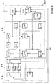
- the clock frequency information acquisition circuit 1.19 comprises a gate circuit 1.31, which can be designed, for example, as an AND gate and which on the one hand transmits a synchronization pulse sequence (SW) sent by the central unit for the bus line 1.14, and on the other hand that oscillator clock signal generated by the oscillator 1.20 is supplied.
- the gate circuit is on the output side 1.31 connected to a clock frequency information counter (TFI counter) 1.32.
- the data transfer clock generator 1.21 comprises a bit duration (T B ) memory 1.33 for a TFI count value determined by the clock frequency information acquisition circuit. This TFI count corresponds to the number of oscillator clocks that were counted during the duration of a synchronization pulse (syn i ).
- the TB memory 1.33 is connected to a T B comparator 1.34, which is connected to a shift register operating as a T B counter 1.35, which is clocked by the oscillator 1.20.
- a delay time (T R ) comparator 1.36 is connected to the T B memory 1.33 via a T R divider 1.37 in order to store a T R count which corresponds, for example, to half the TFI count.
- a second comparator (T R comparator) 1.38 is connected on the one hand to the T R memory 1.36 and on the other hand to a shift register operating as a T R counter 1.39, which is clocked by the oscillator 1.20.
- the output of the T B comparator 1.34 is connected to the reset inputs of the two counters 1.35, 1.39.
- the clock generator 1.18 shown in FIG. 2 works as follows to carry out the method according to the invention:
- the TFI counter 1.32 begins count the oscillator clocks of oscillator 1.20 when the first pulse High arrives.
- the count value present when the pulse drops from high to low corresponds to the duration of the received pulse in relation to the current oscillator frequency of the oscillator 1.20.
- This count value can be transferred to the T B memory 1.33 in order to derive therefrom a clock signal serving as system clock S and a data transfer clock D.
- the synchronization pulse sequence preferably has an alternating level shape, for example an eight-bit synchronization word with the bit sequence 1-0-1-0-1-0-1-0 (HLHLHLHL). It is thus possible to record the duration of the individual H-pulses several times and to obtain an average, and therefore more precise, counting value indicating the pulse duration from the individual counted values, which is then stored in the T B memory 1.33.
- the clock frequency information acquisition circuit 1.19 blocked in this exemplary embodiment by the dead-time circuit at least for the duration of the subsequent data word DW or a predetermined number of data words DW.
- the clock frequency information detecting circuit 1:19 even for a time t tot locked over the duration of the subsequent data word DW and the subsequent data words DW addition, in order to ensure a trouble-free data transfer.
- the count value stored in the T B memory 1.33 is preferably divided by 2 by the T R divider 1.37 and stored in the T R memory 1.36.
- the comparator 1.34 compares the content of the T R counter 1.35 with the count value stored in the T B memory 1.33. As soon as the number of oscillator clocks of the oscillator 1.20 counted by the T B counter 1.35 matches the count value stored in the T B memory 1.33, the comparator 1.34 outputs a system clock signal S to the functional unit 1.24 of the peripheral module.
- the system clock signal is also applied as a reset signal to the counters (1.35, 1.39), so that after the output of the system clock signal S the counting of the oscillator clocks is started again.
- the T R comparator 1.38 To generate the data transfer clock D, which is phase-shifted to the system clock S, by means of the T R comparator 1.38, this compares the number of oscillator oscillations counted by the T R counter 1.39 with the count value stored in the T R memory 1.36. Since the count value stored in the T R memory 1.36 is smaller than the count value stored in the T B memory 1.33, the T R counter 1.39 already reaches this before the expiry, in particular after half the duration of a bit, so that the comparator 1.38 is approximately in outputs a data transfer clock signal D in the middle of a bit. However, the T R counter 1.39 continues to count and is only reset when the system clock S occurs, which coincides with the beginning of a bit in the data word DW.
- the data transfer clock generator 1.18 then generates a system clock S corresponding to the transmission clock of the central unit determined by the clock frequency information during the last data transmission until after the clock frequency information acquisition circuit 1.19 is released, further data transmission from the central unit takes place.
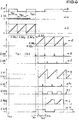
- FIG. 3 now shows in a pulse diagram the time sequence of all important variables of the clock generator 1.18 shown in FIG. 2.
- the label the sizes correspond to the elements and function blocks shown in FIG. 2, that is to say FIG. 4a shows the time profile of the signal level on the BUS line 1.14, FIG. 4b the oscillator clock of the oscillator 1.20, FIG. 4c the counting process in the TFI counter 1.32, FIG. 4d the Counting and comparison processes within the data transfer - clock generator 1.21, FIG. 4e the data transfer clock D from the T R comparator 1.38 and in FIG. 4f the system clock S from the T B comparator 1.34.
- the module receives a first signal pulse syn 11 after a dead time or after connecting the supply voltage, this is forwarded to the TFI counter 1.32 via the gate circuit 1.31.
- the TFI counter 1.32 is reset to zero in a defined manner and now counts the number of oscillator clocks (FIG. 4b) until time T 3.1 , at which the edge of the first synchronization pulse Syn 11 stops.
- the count value of the TFI counter 1.32 present at time t 3.1 is, if appropriate after comparison with permissible value ranges, stored in the TB memory 1.33 as a storage threshold value, which is to be visualized in FIG. 3d.
- the count value determined is divided in parallel in the T R divider 1.37 and stored in the T R memory 1.36 as a second threshold value.
- the counters 1.35 and 1.39 are reset at time t 3.1 and from then on count the oscillator clocks.
- the T R counter 1.39 reaches the threshold value specified in 1.36, so that the comparator 1.38 generates a data transfer clock D (see FIG. 4e).
- the comparator 1.38 generates a data transfer clock D (see FIG. 4e).
- the system clock S (see FIG. 3f) and the counter rely 1:35 and 1:39 back.
- the level of the two synchronization pulses syn 11 and syn 12 shown in FIG. 3 a can also be exchanged if the TFI counter 1.32 or the gate circuit 1.31 also responds to the rising and falling edges accordingly.
- the counting of the oscillator clocks then begins to increase the counts in counters 1.35 and 1.39, the counting values of which are carried out by means of comparators 1.34 and 1.38 with the threshold values specified in memories 1.33 and 1.36, which in turn leads to the following and data clocks are derived.
- the levels of the data pulses D 11 ff. Now carry the information to be transmitted to the control circuit 1.25 or to the output circuit 1.26.
- the levels of the data pulses are each centered using the data transfer clock shown in FIG. 3e scanned. At the end of the first data word DW 1 there is a dead time. At time t 3.9 , a new synchronization pulse sequence SW 2 is received.
- the duration of the synchronization pulses Syn 21 and Syn 22 is different from that of the first synchronization pulse sequence SW 1 .
- the current length of the first synchronization pulse Syn21 is counted in the TFI counter 1.32 by counting the oscillator clocks and, as shown in FIG. 3d, the threshold values are adjusted in the memories 1.33 and 1.36.
- the counters 1.35 and 1.39 are reset and now record the number of oscillator cycles again until the corresponding threshold values are reached, the system and data transfer clock D (see FIGS. 3e and 3f) being generated in each case when the threshold value is reached in comparators 1.34 and 1.38 becomes.
- the decisive factor here is that the clock frequency of the data transfer clock D in FIG. 3e has been adapted in accordance with the now shorter synchronization pulse sequence.
- the adaptation of the transmission frequency only reaches its limits when dimensioning the counters 1.32, 1.35, 1.39, which, however, can be designed accordingly.
- the transmission clock frequency is increased, the relative error in the quantization by means of the oscillator clock also increases, so that a correspondingly high-frequency oscillator must be used.
- FIG. 3 makes it clear that the receiver can be adapted to the transmission frequency over a wide frequency range with simple possibilities.
- FIG 4 shows another clock generator 4.18, which can also be used to carry out the method according to the invention.
- This clock generator 4.18 in turn has a clock frequency information acquisition circuit 4.19, to which the pulses of a pulse sequence indicating the transmit clock, in particular the individual bits of a synchronous word SW, and the output signal of an oscillator 4.20 are supplied.
- the clock frequency information detection circuit 4.20 determines a count value corresponding to the duration of a pulse or bit, which indicates how many oscillator clocks correspond to the duration of a bit. This count is supplied to a variable end ring shift register 40 to set its variable end.
- the ring shift register 40 is from the oscillator 4.20 clocked so that a system clock signal S is output each time the duration of a pulse or bit has expired.
- a phase-locked loop 41 with a phase detector 42, a loop filter 43 and a voltage-controlled oscillator (VCO) 44 is provided to generate the data transfer clock D.
- the output signal of the voltage-controlled oscillator 44 is supplied to the data transfer circuit 4.23 as a data transfer clock D, and is looped back to an input of the phase detector 42.
- a frequency divider 45 can be provided in the feedback line from the voltage-controlled oscillator 44 to the phase detector 42.
- the system clock S is thus generated by means of analog components from a ring shift register with a variable end, which is clocked by the oscillator 4.20 and is set according to a count value corresponding to the duration of a bit.
- the system clock S is phase-shifted by means of a phase-locked loop 41 such that the data transfer takes place approximately in the middle of a bit.
- the clock generator 4.18 is therefore synchronized with the transmission clock of the central unit for each data transmission from the central unit to a peripheral module. This can compensate for long-term drifts as well as temperature and aging-related changes in the oscillator frequency.
- the oscillator 4.20 expediently oscillates at a frequency which is equal to fifty to two hundred times the normal transmit clock frequency.
- the clock generator 2.18 has again as input stage a TFI detection circuit 2.19 which is supplied with the data via the data input of the clock generator 2.18 and the oscillator clocks of an oscillator 2.20 via a reference input, the clock period duration T O of which is substantially shorter than the bit duration T B of the bit pulses of the data and in a typical design of the oscillator is approximately 1/100 of the lowest possible bit duration with which the data blocks are sent.
- the TFI detection circuit 2.19 comprises three TFI counters 2.32 1 , 2.32 2 . 2.33 3 whose counting inputs on these individually assigned pulse outputs of a turnout circuit 2.47 are connected, which in turn forms the input stage of 2.19.
- this turnout circuit 2.47 conveys the falling edge of this first high level pulse T B1 in t 6.1 , and by the rising edge and in t 6.2 the falling edge of the second high level pulse T B3 of the synchronization word falling in t 6.3 in the sense of a sequence control the following functions:
- the number of output pulses of the oscillator 2.20 generated within this time period is counted in the TFI counter 2.32 1 (see FIG. 6c) and the counter reading reached at time t 6.1 entered and saved in a comparison level 2.49.
- the output pulses emitted by the oscillator 2.20 are counted by means of the second TFI counter 2.32 2 , the counter reading reached here at t 6.2 being entered again in the comparison stage 2.49.
- the output pulses of the oscillator 2.20 generated during the bit duration T B3 of the second high level pulse are counted by means of the third TFI counter 2.32 3 and the final counter reading is entered into the comparison stage 2.49, which results from a comparison of the final counter readings of the counters 2.32 based on plausibility criteria 1 , 2.32 2 , 2.33 3 and 2.43 forms a "most probable" numerical value which represents the bit duration T B in units of the period duration T O of the output pulses of the comparison oscillator 2.20.
- this determines the numerical value representing the bit duration T B as the mean value of the counter readings if their scatter is small.
- comparison step 2.49 evaluates that the different meter reading has occurred due to a fault and forms the comparison number as the mean of only the slightly different ones Meter readings.
- the T B reference value representing the bit duration T B is entered at a time t 8.3 in a T B memory 2.33 of a memory unit which, as further memory units, comprises a delay time (TR) memory 2.36 and a duty cycle (TR) memory 2.51 .
- TR delay time
- TR duty cycle
- the content of the T R memory 2.36 is derived from the memory content of the T B memory 2.33 by means of a T R divider 2.37 and thus represents a delay period T R of 25% of the bit duration T B ;
- the memory content of the T A memory 2.51 is derived from the content of the T B memory 2.33 by means of a T R divider 2.50 and thus represents a sampling period T R of 50% of the bit duration T B.
- the clock generator 2.18 comprises a T B counter 2.35 and a T A counter 2.53, to which the output pulses of the oscillator 2.20 are permanently fed as count input pulses, as has already been explained in the first exemplary embodiment.
- the counter After detecting the third synchronization pulse, the counter will be reset 2:35 and 2:53 by example. Via a connecting line between the comparison stage and the T 2:49 2:35 B counter a reset command.
- a system reset line not shown, before the new values are transferred, since such a system reset line is usually already provided .
- the counter reading of the T B counter 2.35 (see FIG. 6d) is continuously compared on the one hand by means of a T B comparator 2.34 with the counter reading of the T B memory 2.33 (threshold value 2.33 in FIG. 6d) characteristic of the bit duration, whereby the T B comparator 2.34 emits a system clock pulse S of short duration each time the counter reading reaches the stored reference value (see FIG. 6e).
- the system cycle distance corresponds in each case to the pulse duration (T B ) last found to be permissible or to a predetermined auxiliary value, the function of which will be explained later.
- the T B counter 2.35 is reset by these system clock pulses of the TB comparator 2.34.
- the counter reading of the first counter 2.61 is continuously compared with the content of the T R memory 2.36 by means of a T R comparator 2.38 (shown as a threshold value 2.36 in FIG. 6d), the T R comparator 2.38 being a reset pulse for the T A counter 2.53 generates utilized pulses of short duration when the counter reading of the T B counter 2.35 is equal to the memory content of the T A memory 2.36 (see Fig. 6f).
- the clock generator 2.18 comprises a duty cycle (T A ) comparator 2.52, which provides a comparison of the count of the T A counter 2.53 with the memory content of the T A memory 2.51, and brief output pulses, the temporal sequence of which is shown in FIG. 6h is generated in each case when the counter reading of the T A counter 2.53 reaches the numerical value stored in the T A memory 2.53, which corresponds to 50% of the bit duration TB in the second exemplary embodiment shown.
- T A duty cycle
- the data transfer circuit 2.27 in FIG. 5 comprises a flip-flop 2.54 as a bistable flip-flop which can be set to a high signal level at its output by the output pulses received at a set input, which are emitted by the T R comparator 2.38. and can be reset to a low signal level at the output by the output pulses of the T A comparator 2.52, which are fed to the flip-flop 2.54 at their reset input.
- the output signal of the flip-flop 2.54 is therefore a sequence of high-level pulses, the duration T A of which corresponds to the sampling period, which in the second exemplary embodiment is half the bit duration T B.
- the time course of the high-level pulses of the flip-flop 2.54 is reproduced qualitatively in FIG. 8i, from which it can be seen that the high-level output pulses start after 25% of the bit duration T B and subside again after 75% of the bit duration T B .
- the data transfer circuit 2.27 comprises a 3-input AND gate 2.55, which outputs a high-level signal at its output if a high signal is also present at each of its three inputs.
- the first input of this AND gate 2.55 is connected to the output of the flip-flop 2.54.
- the clock of the oscillator 2.30 is fed to its second input.
- the third input of the AND gate 2.55 is connected to the data input, via which the data blocks are fed to the respective module.
- the output of the AND gate 2.55 is connected to the count input of a level counter 2.56, which is reset by the system clock pulse.
- the conjunctive linkage of the data sent by the central unit to the output pulses of the oscillator 2.30, on the one hand, and, on the other hand, with the output signals of the flip-flop 2.54, mediated by the AND gate 2.55, thus has the effect that, apart from instabilities in the circuit arrangement as a whole and / or control pulses, the number of which can be regarded as significantly less than the number of output pulses from the reference oscillator 2.20, the counter 2.56 of the data transfer circuit 2.27 counting pulses are only offered when a high signal of a data pulse is present, and that these counting pulses only are fed to the counter 2.56 within the respective sampling period of the duration T A.
- An oversampling occurs within a time window, as will be shown in more detail in FIG. 13 and described later.
- the count after the keying period T A is therefore a measure of the signal level, high or low,
- a level comparator 2.57 which compares and controls the counter reading with or after the end of the scanning period T A with a threshold value which is lower than the maximum achievable counter reading emits a high signal for the duration T B when the processed signal of the supplied data pulse has been a high signal, alternatively a low signal for low signals of the respective by the system clock Data pulse.
- the time course of the data signals emitted by the level comparator 2.57 and taken over for further processing in the control module 2.13 mentioned is reproduced qualitatively in FIG. 6k, from which it is immediately evident that the data transfer and forwarding of the same in the respective control module 2.13 to a retardation leads to a bit duration T B with respect to the received data pulses.
- the threshold above which comparator 2.57 evaluates and outputs the counter reading as a high signal is 50% of the highest possible counter reading without interference pulses of the counter 2.57 (see also Fig. 13).
- the threshold value thus corresponds to the memory content of the T R memory 2.36, so that it can also be used to specify the comparison threshold value with which the level comparator 2.57 compares the counter reading of the counter 2.93.
- control system 2.10 its central unit 2.12 works with transmission clocks which correspond to bit durations T B between 4x10⁻⁶s and 2x10⁻⁵s, and the comparison oscillators 2.30 of the control modules 2.13 are designed for a frequency of 2.5x10⁷s-1.
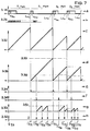
- FIG. 7 shows a pulse diagram of the most important variables in their time profile for the control of a clock generator according to FIG. 5 with PWM signals.
- the TFI counter 3.32 In the clock generator 3.18, the TFI counter 3.32, clocked by the oscillator 3.20, again records the duration of a synchronization pulse (S PWM ), the TFI counter 3.32 corresponding to the shape of PWM signals in each case only on one edge type, in this example on the rising edge reacted at time t 7.0 and t 7.1 .
- the PWM signal shown in FIG. 7a has a first fixed level duration H Fix and, at the end of the PWM word, a second fixed level duration L Fix correspondingly opposite levels, so that regardless of the Iogic content of the PWM information is mandatory a level change occurs, as can be seen in FIG. 7a at time t 7.1 .
- the T R divider 3.37 namely first subtracts the two fixed fixed level duration values from the pulse frame count stored in the T B memory 3.33 and then divides the result by 6, the quotient 6 resulting in exactly half a data pulse of the 3-bit PWM data word.
- the numerical operation stored in the T A divider 3.51 likewise begins with the deduction of the fixed predetermined fixed level duration values, the result of which is then divided by 3 according to the number of bits in the PWM word.
- a delay time to the middle of the first data pulse is again stored in the T R memory 3.36 and the time duration of a data pulse in the T A memory 3.51.
- comparison stage 3.49 triggers a system reset for counters 3.35 and 3.53.
- the T B counter 3.35 now counts the number of oscillator clocks, as shown in FIG. 7d, and at the time t 7.2 in the T R comparator 3.38 reaches the threshold value of the T R memory 3.36, whereupon the T R comparator 3.38 generates a clock signal , as shown in Figure 7e, to the T A counter 3.53.
- the counter 3.53 is in turn reset by this and now counts the number of oscillator cycles up to the threshold value specified by the threshold value in the T A memory 3.51.
- the T A comparator 3.52 then triggers a data transfer clock D (cf. FIG. 7g), with which the downstream data transfer circuit is clocked and at the same time the counter 3.53 is reset. This is repeated in accordance with the number of data pulses in the PWM word.
- the T B counter 3.35 (cf. FIG. 7d) reaches the threshold value stored in the T B memory 3.33, so that the T B comparator 3.34 sets in pulse frame clock.
- the clock frequency is now increased on the transmitter side and a data word D 2, PWM is sent with a shortened data pulse duration.
- the counter 3.32 records the duration of the current data pulse.
- the counter 3.35 continues to run with the old pulse frame duration stored in the memory 3.54.
- the threshold value in the T R memory 3.36 is also based on the old pulse frame spacing, so that the counter 3.53 is started at the time T 7.6 (cf. FIG. 7g). At time T 7.8 , however, the counter 3.32 reaches the end of the PWM data word D 2, PWM and forwards the duration to the comparison stage 3.49, which then resets the counters 3.35 and 3.53 and the new threshold values in the memories 3.33 and 3.36 and 3.51 performing the numerical operation in 3.37 and 3.50.
- the data word D 3, PWM can now be scanned exactly again.
- the T B counter reaches 3:35 at time T 7.9 to now based on the new threshold value of the pulse interval T R -storage 3:36 in T R -Vertician 3.38 whose output clock signal in turn activates the T R counter 3:53 (see FIG. 7g).
- the latter now reaches the threshold value in the T A memory 3.51, which is also adapted to the new pulse frame distance, at time T 7.10 , so that the distance between the data transfer clocks D has now adapted to the new pulse frame distance.
- the loss of a single data pulse which can also be understood as a synchronization pulse, can ultimately shorten the pulse frame duration and thus increase the data transmission frequency.
- This method is also ultimately based on the basic concept already shown in FIG. 5. Only the numerical operation in the dividers 3.37 and 3.50 has to be programmed differently, and instead of the flip-flop 3.55 the output signal of the T a comparator 3.52 must be used as the data transfer clock D.
- FIG. 8 now shows a pulse diagram for an exemplary embodiment in which the transmission frequency and thus the pulse frame spacing changes only by a small amount. This is to be expected in particular whenever thermal or aging-related phenomena change the electrical properties of the transmitting or receiving components. While it is assumed in the following that the clock frequency changes on the transmission side, this example can also be directly transmitted if, for example, the oscillator clock drifts accordingly instead.
- a synchronization pulse S PWM is again sent after a dead time, the length of which is recorded in the TFI counter 3.32 (cf. FIG. C).
- the count value determined is sent to the T B memory 3.33 via the comparison stage 3.49 and from there to the memory 3.36 and 3.51 sent after the numerical operations in 3.37 and 3.50.
- the T B counter 3.35 is reset and the T R comparator 3.38 reaches the threshold value specified in the memory 3.36 at the time T 8.2 . This then triggers a clock on the T A counter 3.53, which is then reset and now also counts the number of oscillator clocks (see FIGS. 8d, f and g).
- the T A counter 3.53 reaches the threshold value specified via the T A comparator 3.52 and stored in the T A memory 3.51, whereupon the T A comparator 3.52 outputs a corresponding clock signal to the flip-flop 3.54.
- the flip-flop 3.54 thus again generates a time window for sampling the data pulse levels, as has already been shown in FIG. 6i in the second exemplary embodiment.
- the duration of the time window is selected across several possible pulse width states of the data word, so that within the pulse frame clock shown in FIG. 8e there is exactly one sampling window from which all possible PWM pulse widths are detected. This is particularly clear in FIG.
- the T B counter 3.35 reaches the threshold value specified by the T B memory 3.33, so that the T B comparator 3.34 sends a new pulse frame clock.
- the current pulse duration deviates, as indicated in FIGS . 8a and 8c.
- the threshold value in the T B memory 3.33 is still based on the old pulse frame distance, so that the T B counter 3.35 already generates the next pulse frame clock at time T 8.7 and resets the counter 3.35.
- the threshold values in memories 3.33, 3.36 and 3.51 have not yet been adapted to the new pulse frame width.
- the TFI counter 3.32 again detects the now new pulse frame distance, resets the T B counter 3.35 again and, based on the new pulse frame distance, gives the corresponding threshold values to the memories 3.33, 3.36 and 3.51, as shown in Figures 8d and 8g is indicated.
- the level comparator 3.57 also adjusts its threshold values S1 to S4 according to the new pulse frame width, as shown in FIG. 8k.
- the T B counter 3.35 reaches the now updated threshold value in the T R memory 3.36 and then triggers the reset of the T R counter 3.53, which follows the time T 8.8 Data pulse is thus again correctly recorded from the time window shown in FIG. 8i.
- FIG. 9 shows in a further pulse diagram the transmission of a pulse-width-modulated signal sequence in which a synchronization pulse is first sent at time T 9.0 , the duration of which is again recorded in TFI counter 3.32 and is stored as a threshold value in T B memory 3.33 at t 9.1 .
- the counters 3.35 and 3.53 again generate the clock signals from which the flip-flop 3.54 (cf. FIG. 9i) derives the sampling time window. If the transmission frequency increases at the time T 9.4 , this is recognized by the T A counter 3.32 at the time T 9.5 and the counters 3.35 and 3.53 are then reset and the threshold values in the memories 3.33, 3.36 and 3.51 are adapted (see FIG. 9d and 9g). From time T 9.5 , the clock generator 3.18 has again taken over the current pulse frame width.
- the transmission clock rate slows down again. While the TFI counter 3.32 already detects the new current pulse width (see Fig. 9c), the counters 3.35 and 3.53 and the memories 3.33, 3.36 and 3.51 still work with the old pulse frame (see Fig. 9d & g). Depending on the strength of the increase or deceleration, this results in a number of incorrect time windows in the flip-flop 3.54 (cf. FIG. 9i). However, since this is a system-inherent error, the transmission side can take this into account, for example, by sending a data signal at this point in time, which can again be interpreted as a synchronization pulse, which does not lead to a critical state in the downstream actuators 11.
- the TFI counter 3:32 reached again the next positive edge, gives the count on the comparison stage 3:43 at the T B -Speicher 3:33 and sets the counters 3.35 and 3:53 back.
- the threshold values in the memories 3.36 and 3.51 are adjusted accordingly, as is shown in FIG. 9.
- the now slow data pulse following the time T 9.10 is again correctly captured by the time window of the flip-flop 3.54 (see FIG. 9k from t 9.11 .
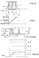
- FIGS. 10 to 13 now show in detail the sequence of the level value detection in the data transfer circuit.
- the amplitude of the strongly disturbed binary signal shown in FIG. 10 on the BUS line 2.14 never reaches the defined target level value 1 ", for example due to line attenuation and interference from the mains voltage.
- the sampling pulses each correspond to a clock of the oscillator which, as already mentioned above, can be used very well for this oversampling due to its high frequency.
- the output pulses of the AND gate 2.55 are then counted in the level value counter 2.56, as shown in FIG. 11. While the first and last sampling pulse do not cause the level value counter 2.56 to increase within the sampling period T a (cf. FIG. 11), the triggering threshold S is nevertheless clearly exceeded.
- the level value counter 2.56 can receive a high signal as a maximum for each sampling pulse to be expressed; minimal of course be zero.
- the basic analogy in the processing of binary and pulse-width-modulated digital signals also becomes clear in the level value acquisition.
- the sampling pulses conjunctively linked in the AND gate 3.55 are incremented in the level value counter 3.56.
- the first and second fixed level durations have been masked out by the delay time T R , so that the level value counter 3.56 can actually be a minimum of zero.
- the counter increment achieved (cf. FIG. 13 3.56) is almost independent of the high-frequency interference, which can be seen as a single peak over time in FIG. 12.
- the optimal values of the individual possible level values are given as 1, 2, 3 , 4 , while the thresholds S 0 to S 3 are each in the middle.
- the testing of the individual thresholds of the level comparator 3.57 again results in 1-0-0-0.
- start bit SB The value of the first data pulse, hereinafter referred to as start bit SB, is of crucial importance. This training is for all procedures binary data transmission, but cannot be used for pulse-width-modulated signals, as will be explained in more detail below.
- a synchronization word SW containing at least one synchronization pulse is normally transmitted or received with a transmission clock frequency T and the data transmission clock D is normally generated from it on the reception side.
- the data transfer clock D which normally corresponds to the transmission clock frequency T in normal operation, is normally applied to the data transfer circuit, and the data word DW is forwarded to the control circuit.
- the control circuit then carries out the necessary operations and, after a transmission delay ⁇ S, sends a response data word A back to the central unit.
- a dead time is started, which is, for example, four or more cycles of the data transfer cycle or the system cycle in the peripheral module and during which the module is not ready to receive. At the end of the dead time, the module is switched to ready to receive again.
- the derivation of the sampling frequency from the synchronous word SW fails, for example as a result of sporadically occurring problems during data transmission, because, for example, an interference pulse together with the data word is sent to the clock via the transmitting / receiving device.
- Generator has arrived, so if there is a synchronization disturbance, the clock generator generates a data transfer clock with an auxiliary sampling frequency which is derived from the sampling frequency last stored and found to be valid.
- auxiliary sampling frequency is multiplied by a predetermined factor, preferably by four, so that a data transfer clock D 4x is generated which is considerably faster than the transmission clock used by the central unit.
- the data transfer clock D 4x is shown schematically in comparison with the data word DW sent by the central unit and the associated transmission clock frequency T normal . It can be seen that, as a result of the data transfer clock D 4x being four times faster, three scans take place during the duration of the start bit SB and the remaining five scans are carried out in such a way that the first bit of the data word is scanned four times and the second bit once.
- the frequency of the system clock corresponds to the sampling frequency used for the functional unit, the subsequent processing of the apparently received data takes place very quickly and the subsequent dead time is greatly shortened, so that the module is switched to ready to receive again very quickly.
- Another advantage of the very fast data transfer in the event of a fault, which is many times faster than the normal data transfer, which is carried out in particular with the four times the sampling frequency, is that a group address for all modules of the system cannot be read if the group address is selected carefully . It is advisable to select 1-0-1-0 as the collective address. Since a bit with the value 1 is interpreted as 1-1-1-1 in the example described four times faster sampling, while a bit with the value 0 is detected as 0-0-0-0, the collective address can also be used for any bit values cannot be incorrectly read in the transmitted data word. Even if the samples assigned to the transmitted address record 2 bits, the bit sequence 1-1-1-0 or 0-0-1-1 can be determined, for example, but not the appropriately selected collective address.
- the method according to the invention for transmitting data can also be used if no start bit is assigned to the data word, as shown in FIG. 14c.
- the data transfer begins after a predetermined waiting time, which follows the end of the synchronous word SW and which lasts for example 2 cycles. Since the data transfer clock D is formed with an increased sampling frequency in the event of a disturbed synchronization, the waiting time until the start of the data transfer is also shortened, as shown in FIG. 14c.
- the signal level present during the last bit of the synchronous word SW, during the time interval between the synchronous word SW and data word DW and during the first bit of the data word DW is sampled, so that, for example the bit sequence is 0-0-0-0-0-0-1-1. In this case too, the collective address cannot be erroneously determined.
- the transmission mode of a module is prevented as soon as, as a result of a disturbance in the transmission of the clock frequency information in the module, it is not only switched to the emergency sampling frequency for generating the data transfer clock in order to be able to switch the module back to receiving as quickly as possible, but simultaneously transmission mode of the module is also blocked. This prevents the module from interfering with the data line.
- a false triggering of protective devices by the modules 20 as a result of a synchronization fault can be ruled out, while the data transmission to the individual modules even in the event of a faulty synchronization in an emergency is perfectly possible. Since the individual modules are very quickly ready to receive again if the clock frequency information is incorrectly transmitted, the central unit can continue its normal self-test or monitoring operation without having to take into account the state of the respective bus line.
Landscapes
- Engineering & Computer Science (AREA)
- Computer Networks & Wireless Communication (AREA)
- Signal Processing (AREA)
- Physics & Mathematics (AREA)
- Spectroscopy & Molecular Physics (AREA)
- Synchronisation In Digital Transmission Systems (AREA)
- Dc Digital Transmission (AREA)
- Small-Scale Networks (AREA)
Applications Claiming Priority (6)
| Application Number | Priority Date | Filing Date | Title |
|---|---|---|---|
| DE19623750A DE19623750A1 (de) | 1996-06-14 | 1996-06-14 | Verfahren zum Übertragen von digitalen Daten |
| DE19623750 | 1996-06-14 | ||
| DE19643205 | 1996-10-19 | ||
| DE19643205A DE19643205C2 (de) | 1996-10-19 | 1996-10-19 | Verfahren zur Übertragung digitaler Daten |
| DE19702271A DE19702271C2 (de) | 1997-01-23 | 1997-01-23 | Verfahren zum Übertragen von Daten in einem System, insbesondere in einem Sicherheitssystem für Kraftfahrzeuge |
| DE19702271 | 1997-01-23 |
Publications (2)
| Publication Number | Publication Date |
|---|---|
| EP0813321A2 true EP0813321A2 (fr) | 1997-12-17 |
| EP0813321A3 EP0813321A3 (fr) | 2001-05-09 |
Family
ID=27216344
Family Applications (1)
| Application Number | Title | Priority Date | Filing Date |
|---|---|---|---|
| EP97108850A Withdrawn EP0813321A3 (fr) | 1996-06-14 | 1997-06-03 | Méthode et système de commande pour la transmission de données numérique |
Country Status (3)
| Country | Link |
|---|---|
| US (1) | US5969631A (fr) |
| EP (1) | EP0813321A3 (fr) |
| JP (1) | JPH10135939A (fr) |
Cited By (10)
| Publication number | Priority date | Publication date | Assignee | Title |
|---|---|---|---|---|
| GB2327324A (en) * | 1997-05-27 | 1999-01-20 | Bosch Gmbh Robert | Back-up clock generating device |
| WO1999050104A1 (fr) * | 1998-03-28 | 1999-10-07 | Robert Bosch Gmbh | Dispositif permettant de commander des equipements de retenue d'un vehicule a l'aide d'unites de traitement des donnees de conception identique |
| US6249558B1 (en) | 1998-03-28 | 2001-06-19 | Temic Telefunken Microeletronic Gmbh | Method for transmitting digital data impulses |
| DE102005001711A1 (de) * | 2005-01-13 | 2006-07-27 | Trw Automotive Gmbh | Elektroniksystem insbesondere für Fahrzeuge und Verfahren zur Reduzierung der Auswirkung elektromagnetischer Strahlung auf Elektroniksysteme in Fahrzeugen |
| EP1315337B1 (fr) * | 2001-10-31 | 2009-08-12 | Infineon Technologies AG | Interface du bus |
| DE102011008227A1 (de) * | 2010-01-18 | 2011-07-28 | Infineon Technologies AG, 85579 | Verfahren und Systeme zum Messen von Datenimpulsen |
| CN110971238A (zh) * | 2019-12-16 | 2020-04-07 | 电子科技大学 | 一种σ-δ型ad的连续等间隙采样的外同步装置 |
| DE102018130360A1 (de) * | 2018-11-29 | 2020-06-04 | Bayerische Motoren Werke Aktiengesellschaft | Verfahren und Vorrichtungen zur Übertragung von Daten über eine elektrische Energieversorgungsleitung |
| WO2023174940A1 (fr) * | 2022-03-14 | 2023-09-21 | Elmos Semiconductor Se | Procédé et appareil de communication de données dans un véhicule entre un appareil d'actionnement et de multiples unités |
| CN118174749A (zh) * | 2024-04-11 | 2024-06-11 | 电子科技大学 | 一种跳时跳频调制器 |
Families Citing this family (51)
| Publication number | Priority date | Publication date | Assignee | Title |
|---|---|---|---|---|
| DE19616293A1 (de) * | 1996-04-24 | 1997-10-30 | Bosch Gmbh Robert | Bussystem für die Übertragung von Nachrichten |
| DE19731116A1 (de) * | 1997-07-19 | 1999-01-28 | Bosch Gmbh Robert | Steuergerät für ein System und Verfahren zum Betrieb eines Steuergerätes |
| FR2786052B1 (fr) * | 1998-11-18 | 2001-02-02 | Gemplus Card Int | Procede de transmission numerique |
| US6389548B1 (en) * | 1999-04-12 | 2002-05-14 | Liam Bowles | Pulse run-length measurement for HF data signal by dividing accumulated phase difference between first and second zero-crossings by single-cycle range using multiple cycle range sawtooth waveform |
| US6647027B1 (en) * | 1999-11-10 | 2003-11-11 | Lsi Logic Corporation | Method and apparatus for multi-channel data delay equalization |
| US6326825B1 (en) * | 2001-01-18 | 2001-12-04 | Agilent Technologies, Inc. | Accurate time delay system and method utilizing an inaccurate oscillator |
| JP2003080910A (ja) * | 2001-06-28 | 2003-03-19 | Pacific Ind Co Ltd | タイヤ状態監視装置 |
| US20030060220A1 (en) * | 2001-09-21 | 2003-03-27 | Hays Nathan J. | Polled tone synchronization of receiver/transmitter units |
| DE10204347A1 (de) * | 2002-02-01 | 2003-08-14 | Atmel Germany Gmbh | Verfahren zur Übertragung von Daten |
| EP1335520B1 (fr) * | 2002-02-11 | 2018-05-30 | Semiconductor Components Industries, LLC | Système de bus multiplexé avec correction du rapport cyclique |
| US7240231B2 (en) * | 2002-09-30 | 2007-07-03 | National Instruments Corporation | System and method for synchronizing multiple instrumentation devices |
| US7072431B2 (en) * | 2002-10-30 | 2006-07-04 | Visteon Global Technologies, Inc. | Clock timing recovery using arbitrary sampling frequency |
| JP4050999B2 (ja) * | 2003-04-18 | 2008-02-20 | 太平洋工業株式会社 | タイヤ状態監視装置 |
| DE10321679B4 (de) * | 2003-05-14 | 2006-11-30 | Siemens Ag | Verfahren und Vorrichtung zur Übertragung von Daten zwischen einem zentralen Steuergerät eines Insassenschutzsystems in einem Fahrzeug und mindestens einer dezentralen Sensoreinheit |
| US7577756B2 (en) | 2003-07-15 | 2009-08-18 | Special Devices, Inc. | Dynamically-and continuously-variable rate, asynchronous data transfer |
| US7203918B2 (en) * | 2003-11-05 | 2007-04-10 | Legend Design Technology, Inc. | Delay and signal integrity check and characterization |
| DE102004006398B4 (de) * | 2004-02-10 | 2006-06-08 | Atmel Germany Gmbh | Verfahren und Vorrichtung zum Synchronisieren einer Funktionseinheit auf eine vorgegebene Taktfrequenz |
| US7516029B2 (en) * | 2004-06-09 | 2009-04-07 | Rambus, Inc. | Communication channel calibration using feedback |
| DE102005014783A1 (de) * | 2005-03-31 | 2006-10-05 | Siemens Ag | Verfahren und Vorrichtungen zum Übertragen von Daten auf eine Datenleitung zwischen einem Steuergerät und zumindest einem dezentralen Datenverarbeitungsgerät |
| US20060247833A1 (en) * | 2005-04-29 | 2006-11-02 | Anupam Malhotra | System and method for remote acquisition of automotive data from a vehicle |
| RU2302701C1 (ru) * | 2005-11-17 | 2007-07-10 | Федеральное государственное унитарное предприятие "Калужский научно-исследовательский институт телемеханических устройств" | Устройство кодовой цикловой синхронизации |
| US20070140399A1 (en) * | 2005-12-20 | 2007-06-21 | International Business Machines Corporation | Phase-locked loop |
| US7478256B2 (en) * | 2006-01-24 | 2009-01-13 | National Instruments Corporation | Coordinating data synchronous triggers on multiple devices |
| DE102006032726B4 (de) * | 2006-07-14 | 2008-05-15 | Lucas Automotive Gmbh | Verfahren zum Synchronisieren von Komponenten eines Kraftfahrzeugbremssystems und elektronisches Bremssteuersystem |
| WO2008015498A1 (fr) * | 2006-08-01 | 2008-02-07 | Freescale Semiconductor, Inc. | Système et procédé de communication de données |
| WO2008056208A1 (fr) * | 2006-11-08 | 2008-05-15 | Freescale Semiconductor, Inc. | Système et procédé de communication de données |
| RU2342795C2 (ru) * | 2007-02-26 | 2008-12-27 | Федеральное государственное унитарное предприятие "Калужский научно-исследовательский институт телемеханических устройств" | Способ цикловой синхронизации блоков информации для диапазона фиксированных скоростей работы в канале связи |
| RU2342796C1 (ru) * | 2007-04-02 | 2008-12-27 | Федеральное государственное унитарное предприятие "Калужский научно-исследовательский институт телемеханических устройств" | Способ кодовой цикловой синхронизации |
| RU2359414C1 (ru) * | 2007-10-30 | 2009-06-20 | Государственное образовательное учреждение высшего профессионального образования-Череповецкий военный инженерный институт радиоэлектроники Министерства обороны Российской Федерации | Способ кодовой цикловой синхронизации |
| US8127170B2 (en) * | 2008-06-13 | 2012-02-28 | Csr Technology Inc. | Method and apparatus for audio receiver clock synchronization |
| RU2383104C2 (ru) * | 2008-08-13 | 2010-02-27 | Федеральное государственное унитарное предприятие "Калужский научно-исследовательский институт телемеханических устройств" | Устройство кодовой цикловой синхронизации |
| RU2401512C1 (ru) * | 2009-03-16 | 2010-10-10 | Федеральное государственное унитарное предприятие "Калужский научно-исследовательский институт телемеханических устройств" | Способ кодовой цикловой синхронизации |
| RU2450465C2 (ru) * | 2009-07-01 | 2012-05-10 | Государственное образовательное учреждение высшего профессионального образования - Череповецкий военный инженерный институт радиоэлектроники Министерства обороны Российской Федерации | Устройство для цикловой синхронизации |
| RU2428801C1 (ru) * | 2010-01-26 | 2011-09-10 | Открытое акционерное общество "Калужский научно-исследовательский институт телемеханических устройств" | Устройство кодовой цикловой синхронизации с мягкими решениями |
| US8307235B2 (en) * | 2010-05-05 | 2012-11-06 | National Instruments Corporation | Cross controller clock synchronization |
| JP4858734B1 (ja) * | 2010-11-10 | 2012-01-18 | 横浜ゴム株式会社 | 送信装置 |
| US8477896B2 (en) * | 2011-01-05 | 2013-07-02 | International Business Machines Corporation | Structure for window comparator circuit for clock data recovery from bipolar RZ data |
| RU2450464C1 (ru) * | 2011-02-24 | 2012-05-10 | Открытое акционерное общество "Калужский научно-исследовательский институт телемеханических устройств" | Устройство кодовой цикловой синхронизации с интегрированными мягкими и жесткими решениями |
| WO2013088173A1 (fr) | 2011-12-14 | 2013-06-20 | Wolfson Microelectronics Plc | Transfert de données |
| CA2882321C (fr) | 2011-12-14 | 2018-05-01 | Wolfson Microelectronics Plc | Transfert de donnees |
| US8799853B2 (en) | 2012-02-17 | 2014-08-05 | National Instruments Corporation | Dynamic synchronization in a target system having multiple programmable hardware elements |
| RU2500074C1 (ru) * | 2012-06-05 | 2013-11-27 | Открытое акционерное общество "Калужский научно-исследовательский институт телемеханических устройств" | Способ кодовой цикловой синхронизации с мягкими решениями |
| JP6492885B2 (ja) * | 2015-03-31 | 2019-04-03 | 日産自動車株式会社 | 診断装置 |
| WO2016202386A1 (fr) * | 2015-06-17 | 2016-12-22 | Telefonaktiebolaget Lm Ericsson (Publ) | Procédé de détection de signal dans un système avec un débit de signal de synchronisation clairsemé |
| US10128783B2 (en) * | 2016-05-31 | 2018-11-13 | Infineon Technologies Ag | Synchronization of internal oscillators of components sharing a communications bus |
| RU2713379C1 (ru) * | 2019-08-20 | 2020-02-05 | Акционерное общество "Концерн "Созвездие" | Устройство синхронизации приёмной и передающей части радиолинии при использовании короткоимпульсных сверхширокополосных сигналов |
| WO2021113636A1 (fr) * | 2019-12-05 | 2021-06-10 | Kennesaw State University Research And Service Foundation, Inc. | Protocole de communication à codage à impulsions variables |
| CN111510111B (zh) * | 2020-04-27 | 2024-03-15 | 上海华虹宏力半导体制造有限公司 | 振荡模块及芯片上电方法 |
| CN115032449A (zh) * | 2022-08-10 | 2022-09-09 | 北京智芯半导体科技有限公司 | 电能计量方法、装置、电子设备、芯片及可读存储介质 |
| CN116299047B (zh) * | 2023-03-31 | 2025-08-22 | 华电山东新能源有限公司枣庄分公司 | 用于风电场集电线路故障监测的异地同步测量系统及方法 |
| CN118900168B (zh) * | 2024-10-08 | 2024-12-13 | 北京芯驰半导体科技有限公司 | 数据传输方法、电子控制单元、计算机程序产品及车辆 |
Family Cites Families (16)
| Publication number | Priority date | Publication date | Assignee | Title |
|---|---|---|---|---|
| US3309463A (en) * | 1963-04-25 | 1967-03-14 | Gen Dynamics Corp | System for locating the end of a sync period by using the sync pulse center as a reference |
| FR2413821A1 (fr) * | 1977-12-28 | 1979-07-27 | Trt Telecom Radio Electr | Dispositif de synchronisation d'un dispositif numerique |
| DE2963491D1 (en) * | 1978-08-16 | 1982-09-30 | Ward Goldstone Ltd | A multiplex information handling system |
| DE2849060C2 (de) * | 1978-11-11 | 1986-10-23 | Telefonbau Und Normalzeit Gmbh, 6000 Frankfurt | Verfahren zur Auswertung von über eine Übertragungsstrecke mittels Impulssignalen unterschiedlicher Länge und Folge gesendeten Informationen |
| GB2043313B (en) * | 1979-02-01 | 1982-10-20 | Ward Goldstone Ltd | Multiplex information handling system |
| US4411007A (en) * | 1981-04-29 | 1983-10-18 | The Manitoba Telephone System | Distributed network synchronization system |
| US4538262A (en) * | 1983-08-03 | 1985-08-27 | Rca Corporation | Multiplex bus system for controlling the transmission of data between a master control unit and a plurality of remotely located receiver-transmitter units |
| JP2579963B2 (ja) * | 1987-10-26 | 1997-02-12 | シャープ株式会社 | 通信方式 |
| US5052026A (en) * | 1989-02-07 | 1991-09-24 | Harris Corporation | Bit synchronizer for short duration burst communications |
| JPH04167738A (ja) * | 1990-10-31 | 1992-06-15 | Nec Corp | 調歩同期通信速度検出装置 |
| FR2676152B1 (fr) * | 1991-05-03 | 1994-10-14 | Renault | Procede, systeme et dispositif de synchronisation des horloges d'un reseau. |
| DE4224508C2 (de) * | 1992-07-24 | 2000-07-06 | Mannesmann Vdo Ag | Verfahren zur Ermittlung der Bittaktfrequenz eines digitalen Signals |
| JPH0738586A (ja) * | 1993-07-21 | 1995-02-07 | Brother Ind Ltd | データ伝送装置 |
| GB2287622B (en) * | 1994-03-17 | 1998-10-28 | Nissan Motor | Multiplex serial data communication circuit network and method and motor control system and method using multiplex serial data communication circuit network |
| JPH0898284A (ja) * | 1994-07-25 | 1996-04-12 | Nippondenso Co Ltd | データ受信装置,送信装置および通信装置 |
| US5594763A (en) * | 1995-06-06 | 1997-01-14 | Cirrus Logic, Inc. | Fast synchronizing digital phase-locked loop for recovering clock information from encoded data |
-
1997
- 1997-06-03 EP EP97108850A patent/EP0813321A3/fr not_active Withdrawn
- 1997-06-12 JP JP9190351A patent/JPH10135939A/ja active Pending
- 1997-06-16 US US08/876,574 patent/US5969631A/en not_active Expired - Fee Related
Cited By (20)
| Publication number | Priority date | Publication date | Assignee | Title |
|---|---|---|---|---|
| GB2327324A (en) * | 1997-05-27 | 1999-01-20 | Bosch Gmbh Robert | Back-up clock generating device |
| GB2327324B (en) * | 1997-05-27 | 2000-07-05 | Bosch Gmbh Robert | Clock-signal generating device and method |
| US6161190A (en) * | 1997-05-27 | 2000-12-12 | Robert Bosch Gmbh | Clock signal loading device and method |
| WO1999050104A1 (fr) * | 1998-03-28 | 1999-10-07 | Robert Bosch Gmbh | Dispositif permettant de commander des equipements de retenue d'un vehicule a l'aide d'unites de traitement des donnees de conception identique |
| US6249558B1 (en) | 1998-03-28 | 2001-06-19 | Temic Telefunken Microeletronic Gmbh | Method for transmitting digital data impulses |
| AU750149B2 (en) * | 1998-03-28 | 2002-07-11 | Robert Bosch Gmbh | Device for controlling restraint devices in an automobile using similarly constructed data processing units |
| EP0948157A3 (fr) * | 1998-03-28 | 2004-01-07 | Conti Temic microelectronic GmbH | Méthode de transmission d' impulsions numériques avec générateur de resynchronisation dirigeant son horloge |
| US6901321B1 (en) | 1998-03-28 | 2005-05-31 | Robert Bosch Gmbh | Device for controlling restraint devices in an automobile using similarly constructed data processing units |
| EP1315337B1 (fr) * | 2001-10-31 | 2009-08-12 | Infineon Technologies AG | Interface du bus |
| DE102005001711A1 (de) * | 2005-01-13 | 2006-07-27 | Trw Automotive Gmbh | Elektroniksystem insbesondere für Fahrzeuge und Verfahren zur Reduzierung der Auswirkung elektromagnetischer Strahlung auf Elektroniksysteme in Fahrzeugen |
| DE102011008227A1 (de) * | 2010-01-18 | 2011-07-28 | Infineon Technologies AG, 85579 | Verfahren und Systeme zum Messen von Datenimpulsen |
| CN102183695A (zh) * | 2010-01-18 | 2011-09-14 | 英飞凌科技股份有限公司 | 用于测量数据脉冲的方法和接收器 |
| US8290094B2 (en) | 2010-01-18 | 2012-10-16 | Infineon Technologies Ag | Methods and systems for measuring data pulses |
| DE102011008227B4 (de) * | 2010-01-18 | 2013-06-06 | Infineon Technologies Ag | Verfahren und Systeme zum Messen von Datenimpulsen |
| CN102183695B (zh) * | 2010-01-18 | 2014-11-12 | 英飞凌科技股份有限公司 | 用于测量数据脉冲的方法和接收器 |
| DE102018130360A1 (de) * | 2018-11-29 | 2020-06-04 | Bayerische Motoren Werke Aktiengesellschaft | Verfahren und Vorrichtungen zur Übertragung von Daten über eine elektrische Energieversorgungsleitung |
| CN110971238A (zh) * | 2019-12-16 | 2020-04-07 | 电子科技大学 | 一种σ-δ型ad的连续等间隙采样的外同步装置 |
| CN110971238B (zh) * | 2019-12-16 | 2023-04-18 | 电子科技大学 | 一种σ-δ型ad的连续等间隙采样的外同步装置 |
| WO2023174940A1 (fr) * | 2022-03-14 | 2023-09-21 | Elmos Semiconductor Se | Procédé et appareil de communication de données dans un véhicule entre un appareil d'actionnement et de multiples unités |
| CN118174749A (zh) * | 2024-04-11 | 2024-06-11 | 电子科技大学 | 一种跳时跳频调制器 |
Also Published As
| Publication number | Publication date |
|---|---|
| EP0813321A3 (fr) | 2001-05-09 |
| JPH10135939A (ja) | 1998-05-22 |
| US5969631A (en) | 1999-10-19 |
Similar Documents
| Publication | Publication Date | Title |
|---|---|---|
| DE3428588C2 (de) | Anlage zum Nachrichtenverkehr im Zeitmultiplex zwischen einer Hauptstation und einer Nebenstation | |
| DE2750818C3 (de) | Anordnung zur zeitmultiplexen Datenübertragung | |
| EP3657734B1 (fr) | Scanneur et indicateur io-link pour le décodage de contenu de communication sur une interface active io-link. | |
| DE3783915T2 (de) | Praediktive taktwiedergewinnungsschaltung. | |
| DE2135890B2 (de) | Synchronisierungsvorrichtung zur Hochprazisionswiedergabe der Phase eines Taktsignals | |
| EP1125406B1 (fr) | Procede et dispositif pour le traitement d'un signal qui transmet des donnees codees | |
| EP0121805B1 (fr) | Synchronisation d'oscillateurs d'horloge qui peuvent être resynchronisés, lors de la transmission de signaux numériques | |
| DE2655443C3 (de) | Vervielfachte Zeitsteuerung zum Erzeugen von Zeitsignalen für Installationen mit signalverarbeitenden Schaltungen | |
| EP1915833A1 (fr) | Procede et dispositif pour decoder un signal | |
| DE69426368T2 (de) | Datenübertragungssystem für ein Kraftfahrzeug | |
| DE3888133T2 (de) | Datenmustersynchronisiereinrichtung. | |
| DE68919211T2 (de) | Empfänger für seriellen Daten. | |
| DE1252727B (de) | Verfahren zum störungsfreien Empfang übertragener Daten | |
| EP1564925B1 (fr) | Procédé et dispositif de synchronisation d'une unité fonctionnelle sur une fréquence d'horloge prédéterminée | |
| DE19732873C2 (de) | Verfahren und Vorrichtung zur Synchronisierung der Datenübertragung zwischen einem dezentralen Satellitengerät und einem zentralen Steuergerät in einem Kraftfahrzeug | |
| DE2457611C3 (de) | Multiplex-Übertragungssystem | |
| DE2926857A1 (de) | Schaltungsanordnung zur ermittlung eines fehlerhaften oszillators in einer schleifenschaltung | |
| DE102009050692B4 (de) | Sicherheits-Kommunikationssystem zur Signalisierung von Systemzuständen | |
| EP0948157B1 (fr) | Méthode de transmission d' impulsions numériques avec générateur de resynchronisation dirigeant son horloge | |
| EP1069690A2 (fr) | Procédé d'échantillonage de signaux digitaux codés en biphase | |
| EP0727897B1 (fr) | Circuit de réception d'un signal transmis sur un bus comme variations d'un niveau de tension | |
| DE2938043C2 (fr) | ||
| DE2021953C3 (de) | Zeitmultiplexübertragungssystem mit einem Sender und einem Empfänger zur Übertragung von Signalen mittels Pulscodemodulation | |
| DE10140741C1 (de) | Vorrichtung zur Erzeugung positionsbasierter Triggersignale für Datenaufnehmer in CT-Gantries | |
| DE4442306A1 (de) | Verfahren und Anordnung zur Ermittlung von Phasenänderungen eines Referenz-Eingangssignals eines Phasenregelkreises |
Legal Events
| Date | Code | Title | Description |
|---|---|---|---|
| PUAI | Public reference made under article 153(3) epc to a published international application that has entered the european phase |
Free format text: ORIGINAL CODE: 0009012 |
|
| AK | Designated contracting states |
Kind code of ref document: A2 Designated state(s): DE ES FR GB IT SE |
|
| RAP1 | Party data changed (applicant data changed or rights of an application transferred) |
Owner name: TEMIC TELEFUNKEN MICROELECTRONIC GMBH |
|
| RIC1 | Information provided on ipc code assigned before grant |
Free format text: 7H 04L 7/04 A, 7H 04L 5/04 B, 7H 04L 25/49 B, 7B 60R 16/02 B, 7H 04L 7/033 B, 7H 04L 25/02 B |
|
| PUAL | Search report despatched |
Free format text: ORIGINAL CODE: 0009013 |
|
| AK | Designated contracting states |
Kind code of ref document: A3 Designated state(s): AT BE CH DE DK ES FI FR GB GR IE IT LI LU MC NL PT SE |
|
| RIC1 | Information provided on ipc code assigned before grant |
Free format text: 7H 04L 7/04 A, 7H 04L 5/04 B, 7H 04L 25/49 B, 7B 60R 16/02 B, 7H 04L 7/033 B, 7H 04L 25/02 B, 7G 08C 15/06 B |
|
| 17P | Request for examination filed |
Effective date: 20010519 |
|
| RAP1 | Party data changed (applicant data changed or rights of an application transferred) |
Owner name: CONTI TEMIC MICROELECTRONIC GMBH |
|
| AKX | Designation fees paid |
Free format text: DE ES FR GB IT SE |
|
| GRAP | Despatch of communication of intention to grant a patent |
Free format text: ORIGINAL CODE: EPIDOSNIGR1 |
|
| STAA | Information on the status of an ep patent application or granted ep patent |
Free format text: STATUS: THE APPLICATION IS DEEMED TO BE WITHDRAWN |
|
| 18D | Application deemed to be withdrawn |
Effective date: 20060808 |