EP0814318B1 - Méthode pour mesurer l'épaisseur et l'index de réfraction des couches constituant une structure laminée et appareil de mesure pour sa mise en oeuvre - Google Patents
Méthode pour mesurer l'épaisseur et l'index de réfraction des couches constituant une structure laminée et appareil de mesure pour sa mise en oeuvre Download PDFInfo
- Publication number
- EP0814318B1 EP0814318B1 EP97109794A EP97109794A EP0814318B1 EP 0814318 B1 EP0814318 B1 EP 0814318B1 EP 97109794 A EP97109794 A EP 97109794A EP 97109794 A EP97109794 A EP 97109794A EP 0814318 B1 EP0814318 B1 EP 0814318B1
- Authority
- EP
- European Patent Office
- Prior art keywords
- laminated structure
- reference mirror
- objective
- beam splitter
- detector
- Prior art date
- Legal status (The legal status is an assumption and is not a legal conclusion. Google has not performed a legal analysis and makes no representation as to the accuracy of the status listed.)
- Expired - Lifetime
Links
Images


Classifications
-
- G—PHYSICS
- G01—MEASURING; TESTING
- G01B—MEASURING LENGTH, THICKNESS OR SIMILAR LINEAR DIMENSIONS; MEASURING ANGLES; MEASURING AREAS; MEASURING IRREGULARITIES OF SURFACES OR CONTOURS
- G01B11/00—Measuring arrangements characterised by the use of optical techniques
- G01B11/02—Measuring arrangements characterised by the use of optical techniques for measuring length, width or thickness
- G01B11/06—Measuring arrangements characterised by the use of optical techniques for measuring length, width or thickness for measuring thickness ; e.g. of sheet material
- G01B11/0616—Measuring arrangements characterised by the use of optical techniques for measuring length, width or thickness for measuring thickness ; e.g. of sheet material of coating
- G01B11/0675—Measuring arrangements characterised by the use of optical techniques for measuring length, width or thickness for measuring thickness ; e.g. of sheet material of coating using interferometry
-
- G—PHYSICS
- G01—MEASURING; TESTING
- G01N—INVESTIGATING OR ANALYSING MATERIALS BY DETERMINING THEIR CHEMICAL OR PHYSICAL PROPERTIES
- G01N21/00—Investigating or analysing materials by the use of optical means, i.e. using sub-millimetre waves, infrared, visible or ultraviolet light
- G01N21/17—Systems in which incident light is modified in accordance with the properties of the material investigated
- G01N21/41—Refractivity; Phase-affecting properties, e.g. optical path length
- G01N21/45—Refractivity; Phase-affecting properties, e.g. optical path length using interferometric methods; using Schlieren methods
Definitions
- the present invention relates to a method measuring the thicknesses and the refractive indices of component layers of a sample laminated structure, and a measuring apparatus for carrying out the same.
- EP-A-0 676 629 discloses a refractive index measurement of the index of refraction of glass without measuring the surface geometry of the glass.
- One embodiment of the measurement system comprises a light source; a beam splitter providing a sample beam and a reference beam; a retroreflector which reflects the reference beam; a holder to hold the material in the path of the sample beam; a detector which detects the reflected reference beam and the reflected sample beam; and an analyzer which determines a position of the translatable retroreflector in response to the detector output signal and which determines the index of refraction of the material in response to the position of the translatable reflector and the thickness of the material.
- a low-coherence interferometry is used for measuring the optical thickness of a transparent sample, such as a thin film or an optical glass.
- the low-coherence interferometry is carried out by an interferometer using white light or light emitted by a low-coherence light source, such as a light emitting diode.
- the low-coherence interferometry finds out the absolute position of a sample from the position of a reference mirror by using a fact that interference fringes appear only near a position where the difference between the two optical path lengths is zero.
- the low-coherence interferometry is applied to the absolute measurement of a block gage, the calibration of a base line and surface protilometry. Recently, active studies on a measuring method developed by extending the low-coherence interferometry have been reported in the fields of ophthalmology and biological science.
- a known confocal laser microscope projects a laser beam on a sample in a spot, and forms an image of reflected light reflected by the sample or fluorescent light emitted by the sample on a point detector.
- the confocal laser microscope as compared with conventional optical microscopes, is capable of forming an image of a high contrast and of forming a three-dimensional image with a high axial resolution, i.e., resolution along the optical axis. Therefore, the confocal laser microscope is used prevalently for measuring the morphology of a surface and observing biological specimens.
- the high axial resolution of the confocal laser microscope is effectively applicable to the measurement of optical thicknesses of component layers of a transparent laminated structure.
- the present invention has been made in view of the problem in the prior art and it is therefore an object of the present invention to provide a method of measuring the thicknesses and the refractive indices of component layer of a laminated structure and a measuring apparatus for carrying out the same.
- a measuring apparatus for measuring thicknesses and refractive indices of component layers of a laminated structure comprises a light source which projects a light beam on the laminated structure, a beam splitter disposed between the light source and the laminated structure, an objective disposed between the point light source and the laminated structure, a reference mirror disposed on a straight line intersecting a straight line connecting the point light source and the laminated structure and passing the beam splitter on one side of the beam splitter, and a detector disposed on the straight line on the other side of the beam splitter.
- the laminated structure and the reference mirror are movable, and a data processing means calculates the thickness and the refractive index of the mth layer of the laminated structure on the basis of a displacement of the laminated structure and that of the reference mirror between a condition where an interference signal reaches a maximum when one of the surfaces of the mth layer is at the first focal point of the objective, and a condition where an interference signal reaches a maximum when the other surface of the mth layer is at the second focal point of the objective indicated by confocal signals and interference signals provided by the detector.
- the laminated structure and the reference mirror are moved from the first focal point and the first reference mirror position to the second focal point and the second reference mirror position, respectively, on the basis of the confocal signal provided by the detector upon the reception of the reflected light beam and the interference signal provided by the detector upon the reception of the reflected light beam and the reference light beam, and the thickness and the refractive index of the mth layer of the laminated structure are determined on the basis of the respective displacements of the laminated structure and the reference mirror.
- a measuring apparatus 10 for measuring thicknesses and refractive indices of component layers of a laminated structure comprises a point light source 11 (low-coherence light source) which projects a light beam through a pinhole 11a on a sample 15, i.e., a laminated structure, and collimator lens 12, a beam splitter 13 and an objective 14 arranged in that order between the point light source 11 and the sample 15.
- a reference mirror 16 is disposed on a straight line L 2 intersecting a straight line L 1 interconnecting the point light source 11 and the sample 15 on one side of the beam splitter 13.
- a condenser lens 17, and a detector 18 provided with a pinhole 18a are disposed on the straight line L 2 on the other side of the beam splitter 13.
- the optical system of the measuring apparatus 10 shown in Fig. 1A is a combination of a Michelson interferometer and a confocal system.
- the light beam emitted by the point light source 11 is focused on the sample 15 by the objective 14 disposed near the sample 15.
- the light beam reflected by the sample 15 is gathered by the condenser lens 17 on the pinhole 18a, and the light beam transmitted through the pinhole 18a is detected by the detector 18.
- the point light source 11, the objective 14 and the detector 18 constitute the confocal system.
- the measuring apparatus 10 using the point light source 11 which emits a light beam of a wide wavelength spectral width serves as a low-coherence interferometer.
- the sample 15 shown in Fig. 1A is a transparent laminated structure.
- the optical system functions as a confocal system when the reference mirror 16 is screened to block a reference optical path.
- the light beam emitted by the point light source 11 travels through the collimator lens 12, the beam splitter 13 and the objective 14 to the sample 15.
- the reflected light beam reflected by the sample 15 travels through the objective 14, the beam splitter 13 and the condenser lens 17 to the detector 18.
- the detector Upon the reception of the reflected light beam, the detector provides a confocal signal.
- a peak appears in the output of the detector 18 upon the arrival of an interface between the adjacent component layers of the sample 15 at a focal point of the objective 14.
- peaks appear successively in the output of the detector 18 as the interfaces between the adjacent component layers of the sample 15 arrive at a focal point of the objective 14 successively, as indicated by peaks on the Z-axis of the graph of Fig. 2.
- the arrival of each interface at the focal point of the objective 14 can be known from the peak in the output signal of the detector.
- the sample 15 When the sample 15 is fixedly disposed with the mth interface, i.e., an interface between layers of (m-1)th and mth from the surface of the sample 15 facing the objective 14, positioned at the focal point of the objective 14 as shown in Fig. 1B and the reference mirror 16 is unscreened, the reflected light beam reflected by the sample 15 travels through the objective 14, the beam splitter 13 and the condenser lens 17 to the detector 18, and part of the light beam emitted by the point light source 11 travels, as a reference light beam, through the collimator lens 12, the beam splitter 13, the reference mirror 16 and the condenser lens 17 to the detector 18. Then, the detector 18 provides an interference signal on the basis of the reflected light beam and the reference light beam. In this state, the sample 15 is positioned at a first position.
- the mth interface i.e., an interface between layers of (m-1)th and mth from the surface of the sample 15 facing the objective 14, positioned at the focal point of the objective 14 as
- the reference mirror 16 is then moved to a first reference mirror position where the reference light beam makes the amplitude of the interference signal increase to a maximum. In this state, the optical path difference between the two optical paths of the interferometer is zero.
- the sample 15 is advanced toward the objective 14 by a distance ⁇ Z m to focus the light beam on the (m+1)th interface as shown in Fig. 1C.
- the (m+1)th interface is at the focal point of the objective 14.
- the sample 15 is positioned at a second position but the condition for equal optical path length is not met because the position of the reference mirror 16 is not changed. Therefore, the reference mirror 16 is moved by a distance ⁇ l m to a second reference mirror position to reduce the optical path difference to zero.
- an optical path length i.e., (refractive index) ⁇ (thickness)
- ⁇ thickness
- the focal point is moved from the mth interface to the (m+1)th interface by the confocal optical system as shown in Fig. 3, in which the objective 14 is shifted to simplify the procedure for making the expressions.
- the (m+1)th interface is positioned at the focal point, all the intersection points of marginal rays and each interface are translated evenly away from the optical axis. From Fig.
- p is the displacement of the intersection point of the marginal rays and the interface
- ⁇ 0 is the incident angle of the peripheral rays on the first layer
- ⁇ m is the refractive angle at the mth interface
- d m is the geometrical thickness of the mth layer.
- Conditions for establishing an equal optical path length state i.e., a state in which the optical path length of two optical paths are equal to each other, by the low-coherence interference method will be considered.
- the conditions for the equal optical path length state become unsatisfied when the sample 15 is shifted.
- the geometrical thickness d m and the refractive index n m of the mth layer are determined by solving simultaneous equations (3) to (5).
- d m ⁇ l m + ⁇ Z m n m
- This procedure is repeated for the successive layers to determine the respective geometrical thicknesses and the respective refractive indices of the layers.
- a laser diode (TOLD-9150, threshold current: 52 mA, available from Toshiba) was employed as the point light source 11 and the laser diode was driven by a current below the threshold current to use the laser diode as a light emitting diode.
- a light beam emitted by the point light source 11 has a wide spectrum and hence the point light source 11 functions as a low-coherence light source. Since the point light source 11 has a minute light emitting region the point light source 11 need not be provided with the pinhole lla. The characteristics of the point light source 11 will be explained in terms of measured spectrum and measured coherence length.
- Fig. 4 shows the spectrum of the light beam emitted by the point light source when a current of 30 mA was supplied to the point light source 11, in which center wavelength is 690.5 nm and the full width at half maximum of the spectrum is 15.3 nm.
- the emission power was 50 ⁇ W.
- Fig. 5 shows the current dependence of the center wavelength and the full width at half maximum of the spectrum. It is known from Fig.
- Coherence length was measured by a Michelson interferometer shown in Fig. 6, in which a plane mirror 16a was moved along an optical axis.
- a point light source 11 is driven by a driving unit 20, the plane mirror 16a is mounted on a linear stage 28 driven by a stepping motor.
- the operation of the driving unit 20 and the linear stage 28 is controlled by a controller 21.
- a detector 18 is connected to a personal computer 22 controlling the controller 21.
- Fig. 7A shows an interferogram when a current of 30 mA was supplied to the point light source 11.
- the plane mirror 16a was moved stepwise in steps of 0.1 ⁇ m.
- the full width at a half maximum, i.e., the coherence length, was 6.9 ⁇ m.
- the current was varied in a current range below the threshold current for the same measurement to examine the current dependence of the coherence length.
- the results are shown in Fig. 7B. It is known from Fig. 7B that the coherence length varies scarcely when the current is below 35 mA, and increases sharply with the current after the current in creases beyond the threshold current.
- a driving current of 30 mA was used taking into consideration the output power of the laser diode, i.e., the point light source, and the coherence length.
- a collimator lens 12 collimates rays of a light beam emitted by a point light source, i.e., a laser diode.
- the collimated light beam travels through a beam splitter 13 is focused on a sample 15 by a objective 14 (MD Plan, magnification: ⁇ 10, Effective N.A.: 0.21, W.D.: 7 mm, Olympus).
- the light beam reflected by the beam splitter 13 is used as a reference light beam.
- the reflected light beam is gathered on a pinhole 18a of 10 ⁇ m in diameter by a condenser lens 17, and the light beam traveled through the pinhole 18a is detected by a detector 18, i.e., a photomultiplier tube (Optical Sensor Module H5783-01, Hamamatsu Photonics).
- the output signal of the detector 18 is monitored by an oscilloscope 27 and is given through an AD board, not shown, to a personal computer 22.
- the sample 15 and a reference mirror 16 are mounted on linear stages 27 and 28 driven by stepping motors, respectively.
- the linear stages 27 and 28 can be moved in steps of 1 ⁇ m and 0.1 ⁇ m, respectively, by giving pulse signal through a PIO board, not shown, by the personal computer to a controller 21.
- a shutter 25 and a variable aperture 26 are disposed on the optical path of the reference light beam.
- the intensity of the reference light beam is regulated by regulating the diameter of the reference light beam by the variable aperture 26.
- the laser diode serving as the point light source 11 is made to perform laser oscillation when adjusting the optical system, and a current not higher than the threshold current is supplied to the laser diode to use the laser diode as a light emitting diode for measurement
- the sample 15 is disposed close to the objective 14, and then the sample 15 is moved away from the objective 14 to prevent the sample 15 from coming into contact with the objective 14.
- the reference light beam is intercepted by the closed shutter 25.
- the position of a peak is determined by subjecting a confocal signal to smoothing differentiation.
- the position of the sample 15 is adjusted on the basis of the data representing the position of the peak so that a surface thereof nearest to the objective 14 is positioned at the focal point of the objective 14.
- the shutter 25 is opened the gain of the photomultiplier of the detector 18 and the reference mirror 16 is moved away from the beam splitter 13 for a scanning operation.
- the sample 15 and the reference mirror 16 are returned to their initial positions, respectively, the sample 15 is moved again on the basis of the data representing the position of the peak so that the next interface is positioned at the focal point, and then the reference mirror 16 is moved again for a scanning operation.
- the foregoing procedure is repeated for all the interfaces of the sample 15.
- the return of the sample 15 and the reference mirror 16 to their initial positions takes an additional time, the influence of backlashes in the linear stages 27 and 28 can be reduced.
- the detection of the position of the peak of the confocal signal for the analysis of signals was carried out in an on-line mode, and the interferogram was analyzed after transferring the data to a work station.
- the optical plane mirror 16a (Fig. 6) was used for measurement to confirm if the optical system is functioning as both the confocal system and the low-coherence interferometer.
- Fig. 9A shows the axial response of the confocal system when the optical plane mirror 16a, i.e., the sample, was moved.
- An interferogram as shown in Fig. 9B was obtained by fixedly holding the optical plane mirror 16a at a position corresponding to the peak in the output signal of the detector 18, and moving the reference mirror 16. Full widths at half maximum determined from those results were 20 ⁇ m and 46 ⁇ m. It is known from Fig. 9B that the interferogram, as compared with the interferogram shown in Fig.
- liquid crystal cell three-layer liquid crystal evaluation glass cell
- thirteen-layer sample fabricated by stacking cover glasses were subjected to measurement. Measurements of the three-layer liquid crystal cell and the thirteen-layer sample are given below by way of example.
- a sample liquid crystal cell 15 (EHC K.K.) was fabricated by combining two glass plates 30 and 31 of 0.7 mm in thickness and 1.51 in refractive index so that a 50 ⁇ m thick space 32 was formed between the glass plates 30 and 31.
- the space 32 was kept void for a condition A, and the space 32 was filled up with pure water for a condition B.
- Figs. 11A to 11D show measured results.
- Figs. 11A and 11B show the results of measurement under the condition A
- Figs. 11C and 11D show the results of measurement under the condition B.
- FIG. 11A and 11C show data representing the response of the confocal system, in which peaks 1, 2, 3 and 4 are the output signals of the detector when the light beam was focused on the interfaces indicated by the same numerals, respectively.
- Figs. 11B and 11D show interferograms, in which numerals indicating the interferograms corresponds to positions of the sample liquid crystal at which the peaks indicated by the same numerals shown in Figs. 11A and 11C appear, respectively.
- Figs. 11A and 11B shows the signals after adjusting the bias properly to facilitate understanding.
- the values of the peaks 2 and 3 in Fig. 11C are small as compared with those of the corresponding peaks 2 and 3 in Fig.
- Figs. 12B and 12C shown measured confocal signals and interferograms, respectively.
- numerals indicating peaks corresponds to those indicating interfaces in Fig. 12A.
- the interferograms shown in Fig. 12C are produced after adjusting the bias.
- Figs. 12B and 12C shown measured confocal signals
- the peaks indicated by greater numerals have smaller values because the quantity of light absorbed by the layers and the quantity of light reflected by the interfaces increases with depth from the surface of the sample 15 facing the objective 14 and hence the quantity of light reflected by the interface and falling on the detector 18 decreases with the depth of the interface from the surface of the sample 15 facing the objective 14.
- the interferograms relating to the deeper layers are distorted by color dispersion caused by the forward layers. The localization of the interferogram relating to the interfaces of the air layers do not change for the same reasons as those for the liquid crystal cell.
- Table 1 shows the geometrical thicknesses and the refractive indices of the samples 15 calculated by using the data about the intervals between the peaks and the intervals between the localized interference fringes, and Expressions (6) and (7). Shown also in Table 1 are data about the other samples 15, thicknesses measured by a micrometer and nominal values shown in catalogs. With the samples 15 of 1 mm or above in thickness, those data coincide with each other with an error of 1% or below. Relative accuracy deteriorates when the thickness of the sample 15 decreases, which is supposed to occur because errors in the estimation of the position for equal optical path length are most effective in introducing errors into the final thickness and the refractive index.
- the present invention could measure accurately the thicknesses and refractive indices of the component layers of the samples 15 of laminated structures in which the opposite surfaces of each component layer are not exactly parallel to each other and each component layer has nonuniform thickness, such as an onion.
- the component layers of the sample 15 may be of a material other than glass, such as a synthetic resin or the like, provided that the component layers are transparent to light of wavelength in the wavelength range of the light emitted by the point light source 11. If a laser diode which emits light of a wavelength in the near-infrared wavelength range is employed as the point light source 11, the present invention is applicable to the measurement of the thicknesses and the refractive indices of the component layers of semiconductor structures.
- the sample and the reference mirror are moved from a first confocal position and a first reference mirror position for a first surface of the mth layer of the sample to a second confocal position and a second reference mirror position for a second surface of the mth layer, respectively.
- the thickness and the refractive index of the mth layer are determined on the basis of the respective displacements of the sample and the reference mirror.
Landscapes
- Physics & Mathematics (AREA)
- General Physics & Mathematics (AREA)
- Health & Medical Sciences (AREA)
- Life Sciences & Earth Sciences (AREA)
- Chemical & Material Sciences (AREA)
- Analytical Chemistry (AREA)
- Biochemistry (AREA)
- General Health & Medical Sciences (AREA)
- Immunology (AREA)
- Pathology (AREA)
- Length Measuring Devices By Optical Means (AREA)
- Investigating Or Analysing Materials By Optical Means (AREA)
Claims (6)
- Appareil de mesure pour mesurer les épaisseurs et les indices de réfraction de couches de composants d'une structure stratifiée (15), en combinaison avec une structure stratifiée (15), ledit appareil de mesure comprenant :dans lequel la structure stratifiée (15) est mobile le long de l'axe optique de l'objectif (14) ; le miroir de référence (16) est mobile le long de son axe optique, etune source de lumière (11) qui projette un faisceau de lumière sur la structure stratifiée (15) ;un séparateur de faisceau (13) disposé entre la source de lumière (11) et la structure stratifiée (15) ;un objectif (14) disposé entre le séparateur de faisceau (13) et la structure stratifiée (15) ;un miroir de référence (16) disposé sur un côté du séparateur de faisceau (13) et situé sur une première ligne droite (L2) qui croise au niveau du séparateur de faisceau (13) une deuxième ligne droite (L1) reliant la source de lumière (11) avec la structure stratifiée (15) ; etun détecteur (18) disposé sur la première ligne droite (L2) sur l'autre côté du séparateur de faisceau (13) par rapport au miroir de référence (16) ;
un moyen de traitement de données (22) pour calculer l'épaisseur et l'indice de réfraction d'une mième couche de la structure stratifiée (15) sur la base d'un déplacement de la structure stratifiée (15) et de celui du miroir de référence (16) entre une condition où une des surfaces de la mième couche est à un point focal de l'objectif (14) et un signal d'interférence fourni par le détecteur (18) atteint un maximum, et une condition où l'autre surface de la mième couche est au point focal de l'objectif (14) et un signal d'interférence fourni par le détecteur (18) atteint un maximum. - Appareil de mesure selon la revendication 1, dans lequel
le moyen de traitement des données (22) est conçu pour calculer l'épaisseur dm et l'indice de réfraction nm de la mième couche en utilisant les expressions :
- Appareil de mesure selon la revendication 1, dans lequel
les surfaces opposées d'au moins une de la pluralité de couches de la structure stratifiée (15) ne sont pas parallèles les unes par rapport aux autres, et l'épaisseur de la même couche varie sur la zone entière de la structure stratifiée (15). - Procédé pour mesurer les épaisseurs et les indices de réfraction de couches de composants d'une structure stratifiée (15) en utilisant un appareil de mesure comprenant : une source de lumière (11) qui projette un faisceau de lumière sur la structure stratifiée (15), un séparateur de faisceau (13) disposé entre la source de lumière (11) et la structure stratifiée (15), un objectif (14) disposé entre le séparateur de faisceau (13) et la structure stratifiée (15), un miroir de référence (16) disposé sur un côté du séparateur de faisceau (13) et situé sur une première ligne droite (L2) qui croise au niveau du séparateur de faisceau (13) une deuxième ligne droite (L1) reliant la source de lumière (11) avec la structure stratifiée (15) ; et un détecteur (18) disposé sur la première ligne droite (L2) sur l'autre côté du séparateur de faisceau (13) par rapport au miroir de référence (16) ; dans lequel la structure stratifiée (15) est mobile le long de l'axe optique de l'objectif (14), le miroir de référence (16) est mobile le long de son axe optique ; ledit procédé comprenant les étapes consistant à :projeter un faisceau de lumière à l'aide de lumière (11) à travers le séparateur de faisceau (13) et l'objectif (14) sur la structure stratifiée (15) ;déplacer la structure stratifiée (15) et le miroir de référence (16) sur la base d'un signal confocal fourni par le détecteur (18) pendant la réception du faisceau de lumière réfléchi déplacé de la structure stratifiée (15) vers le détecteur (18) par l'intermédiaire du séparateur de faisceau (13) et d'un signal d'interférence fourni par le détecteur (18) pendant la réception du faisceau de lumière réfléchi et d'un faisceau de lumière de référence se déplaçant à travers le séparateur de faisceau (13) et du miroir de référence (16) vers le détecteur (18) de sorte qu'une des surfaces de la mième couche de la structure stratifiée (15) est positionnée à un point focal de l'objectif (14) et que le miroir de référence (16) est positionné à une première position du miroir de référence (16) de sorte que le signal d'interférence atteint un maximum ;déplacer la structure stratifiée (15) et le miroir de référence (16) sur la base du signal confocal et du signal d'interférence fourni par le détecteur (18) de sorte que l'autre surface de la mième couche de la structure stratifiée (15) est positionnée au point focal de l'objectif (14) et que le miroir de référence (16) est positionné à une deuxième position du miroir de référence (16) de sorte que le signal d'interférence atteint un maximum ; etdéterminer l'épaisseur et l'indice de réfraction de la mième couche de la structure stratifiée (15) sur la base d'un déplacement de la structure stratifiée (15) pour former une première position où une surface de la mième couche est au point focal de l'objectif (14) vers une deuxième position où l'autre surface de la mième couche est au point focal de l'objectif (14), et un déplacement du miroir de référence (16) de la première position du miroir de référence (16) vers la deuxième position du miroir de référence (16).
- Procédé selon la revendication 4, dans lequel
le procédé pour déterminer l'épaisseur et l'indice de réfraction de la mième couche les détermine en utilisant les expressions :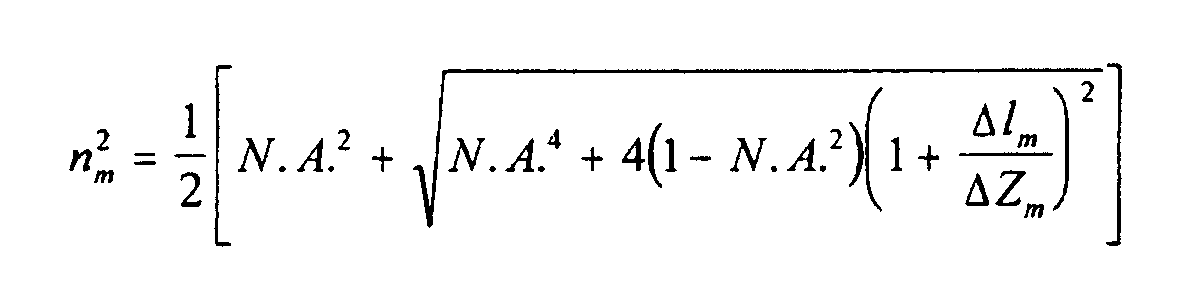
- Procédé selon la revendication 4, dans lequel la structure stratifiée (15), une pluralité de couches, les surfaces opposées d'au moins une de la pluralité de couches de la structure stratifiée (15) ne sont pas parallèles les unes par rapport aux autres, et l'épaisseur de la même couche varie sur la zone entière de la structure stratifiée (15).
Applications Claiming Priority (3)
| Application Number | Priority Date | Filing Date | Title |
|---|---|---|---|
| JP155828/96 | 1996-06-17 | ||
| JP15582896A JP3459327B2 (ja) | 1996-06-17 | 1996-06-17 | 積層構造体の層厚および屈折率の測定方法およびその測定装置 |
| JP15582896 | 1996-06-17 |
Publications (3)
| Publication Number | Publication Date |
|---|---|
| EP0814318A2 EP0814318A2 (fr) | 1997-12-29 |
| EP0814318A3 EP0814318A3 (fr) | 1999-11-10 |
| EP0814318B1 true EP0814318B1 (fr) | 2002-08-28 |
Family
ID=15614389
Family Applications (1)
| Application Number | Title | Priority Date | Filing Date |
|---|---|---|---|
| EP97109794A Expired - Lifetime EP0814318B1 (fr) | 1996-06-17 | 1997-06-16 | Méthode pour mesurer l'épaisseur et l'index de réfraction des couches constituant une structure laminée et appareil de mesure pour sa mise en oeuvre |
Country Status (4)
| Country | Link |
|---|---|
| US (1) | US5943134A (fr) |
| EP (1) | EP0814318B1 (fr) |
| JP (1) | JP3459327B2 (fr) |
| DE (1) | DE69714915T2 (fr) |
Cited By (2)
| Publication number | Priority date | Publication date | Assignee | Title |
|---|---|---|---|---|
| CN102175426A (zh) * | 2011-02-15 | 2011-09-07 | 北京理工大学 | 共焦干涉定焦及曲率半径测量方法 |
| CN107401982A (zh) * | 2017-07-26 | 2017-11-28 | 淮阴师范学院 | 基于低相干光干涉法的透镜中心厚度的非接触测量方法 |
Families Citing this family (66)
| Publication number | Priority date | Publication date | Assignee | Title |
|---|---|---|---|---|
| JP3582311B2 (ja) * | 1996-08-04 | 2004-10-27 | 松下電器産業株式会社 | 媒質の測定方法および測定装置 |
| JPH11344312A (ja) * | 1998-06-01 | 1999-12-14 | Jasco Corp | 液晶セルギャップ測定方法及びその装置 |
| JP3704952B2 (ja) * | 1998-06-03 | 2005-10-12 | 松下電器産業株式会社 | 媒質の測定装置および測定方法 |
| JP3569726B2 (ja) * | 1998-12-15 | 2004-09-29 | 独立行政法人理化学研究所 | 試料の幾何学的厚さおよび屈折率測定装置およびその測定方法 |
| JP2000241128A (ja) * | 1998-12-25 | 2000-09-08 | Olympus Optical Co Ltd | 面間隔測定方法および装置 |
| TW477897B (en) * | 1999-05-07 | 2002-03-01 | Sharp Kk | Liquid crystal display device, method and device to measure cell thickness of liquid crystal display device, and phase difference plate using the method thereof |
| JP4060494B2 (ja) * | 1999-08-30 | 2008-03-12 | アンリツ株式会社 | 三次元表面形状測定装置 |
| JP3642996B2 (ja) * | 1999-11-18 | 2005-04-27 | 独立行政法人科学技術振興機構 | 光干渉法による測定対象物の屈折率と厚さの同時測定方法及びそのための装置 |
| US6368881B1 (en) * | 2000-02-29 | 2002-04-09 | International Business Machines Corporation | Wafer thickness control during backside grind |
| KR100421427B1 (ko) * | 2001-01-11 | 2004-03-09 | 한국과학기술원 | 공초점원리의 단위변위센서를 이용한 초정밀 변위측정기및 다양한 변위측정방법 |
| US6462823B1 (en) * | 2001-04-13 | 2002-10-08 | Agilent Technologies, Inc. | Wavelength meter adapted for averaging multiple measurements |
| JP2002323659A (ja) * | 2001-04-25 | 2002-11-08 | Olympus Optical Co Ltd | 共焦点光学系及びこれを用いた走査型共焦点顕微鏡 |
| US6731380B2 (en) | 2001-06-18 | 2004-05-04 | Applied Optics Center Of Delaware, Inc. | Method and apparatus for simultaneous measurement of the refractive index and thickness of thin films |
| DE10141544A1 (de) * | 2001-08-24 | 2003-03-13 | Eppendorf Ag | Vorrichtung zur Behandlung von Flüssigkeiten und Verfahren zum Betreiben der Vorrichtung |
| UA74801C2 (en) * | 2002-05-20 | 2006-02-15 | Swedish Lcd Ct | Method for measuring the parameters of a liquid crystal cell |
| US7869057B2 (en) | 2002-09-09 | 2011-01-11 | Zygo Corporation | Multiple-angle multiple-wavelength interferometer using high-NA imaging and spectral analysis |
| KR101223195B1 (ko) * | 2002-09-09 | 2013-01-21 | 지고 코포레이션 | 박막 구조의 특징화를 포함하여, 타원편광 측정, 반사 측정 및 산란 측정을 위한 간섭측정 방법 및 장치 |
| US7139081B2 (en) | 2002-09-09 | 2006-11-21 | Zygo Corporation | Interferometry method for ellipsometry, reflectometry, and scatterometry measurements, including characterization of thin film structures |
| US7116429B1 (en) * | 2003-01-18 | 2006-10-03 | Walecki Wojciech J | Determining thickness of slabs of materials by inventors |
| US7324214B2 (en) | 2003-03-06 | 2008-01-29 | Zygo Corporation | Interferometer and method for measuring characteristics of optically unresolved surface features |
| JP4051443B2 (ja) * | 2003-03-20 | 2008-02-27 | 独立行政法人産業技術総合研究所 | 光学材料の群屈折率精密計測方法及び装置 |
| US7233401B1 (en) | 2003-07-11 | 2007-06-19 | Foothill Instruments, Llc | Method and apparatus for measuring thickness of a material |
| JP4194971B2 (ja) * | 2004-04-16 | 2008-12-10 | 日本電信電話株式会社 | 屈折率測定方法及びその装置並びに屈折率測定・硬化装置 |
| US7142311B2 (en) * | 2004-05-18 | 2006-11-28 | Zygo Corporation | Methods and systems for determining optical properties using low-coherence interference signals |
| CN1321322C (zh) * | 2004-08-30 | 2007-06-13 | 浙江大学 | 测量三维折射率的微分干涉层析方法及其测量仪 |
| US7884947B2 (en) | 2005-01-20 | 2011-02-08 | Zygo Corporation | Interferometry for determining characteristics of an object surface, with spatially coherent illumination |
| US7428057B2 (en) * | 2005-01-20 | 2008-09-23 | Zygo Corporation | Interferometer for determining characteristics of an object surface, including processing and calibration |
| US8362431B2 (en) | 2005-03-15 | 2013-01-29 | Mount Holyoke College | Methods of thermoreflectance thermography |
| JP4203831B2 (ja) * | 2006-11-30 | 2009-01-07 | 独立行政法人産業技術総合研究所 | 光学材料の群屈折率精密計測方法 |
| WO2008080127A2 (fr) | 2006-12-22 | 2008-07-03 | Zygo Corporation | Appareil et procédé de mesure des caractéristiques d'objets géographiques de surface |
| US7889355B2 (en) | 2007-01-31 | 2011-02-15 | Zygo Corporation | Interferometry for lateral metrology |
| JP4939304B2 (ja) * | 2007-05-24 | 2012-05-23 | 東レエンジニアリング株式会社 | 透明膜の膜厚測定方法およびその装置 |
| US7619746B2 (en) | 2007-07-19 | 2009-11-17 | Zygo Corporation | Generating model signals for interferometry |
| WO2009064670A2 (fr) | 2007-11-13 | 2009-05-22 | Zygo Corporation | Interferomètre à balayage de polarisation |
| JP5042791B2 (ja) * | 2007-11-30 | 2012-10-03 | オリンパス株式会社 | 膜厚測定装置 |
| US8126677B2 (en) | 2007-12-14 | 2012-02-28 | Zygo Corporation | Analyzing surface structure using scanning interferometry |
| JP5274862B2 (ja) * | 2008-03-10 | 2013-08-28 | 東京エレクトロン株式会社 | 温度測定装置及び温度測定方法 |
| US10646116B2 (en) | 2013-07-25 | 2020-05-12 | Amo Development, Llc | In situ determination of refractive index of materials |
| US8120781B2 (en) | 2008-11-26 | 2012-02-21 | Zygo Corporation | Interferometric systems and methods featuring spectral analysis of unevenly sampled data |
| JP5397817B2 (ja) * | 2010-02-05 | 2014-01-22 | 国立大学法人名古屋大学 | 干渉測定装置および測定方法 |
| GB2478590A (en) | 2010-03-12 | 2011-09-14 | Precitec Optronik Gmbh | Apparatus and method for monitoring a thickness of a silicon wafer |
| JP5500354B2 (ja) * | 2010-03-30 | 2014-05-21 | 株式会社ニコン | 膜構造測定方法及び表面形状測定装置 |
| JP4912504B1 (ja) * | 2010-09-16 | 2012-04-11 | キヤノン株式会社 | 屈折率の計測方法および計測装置 |
| CN102147240B (zh) * | 2010-12-24 | 2012-08-22 | 北京理工大学 | 差动共焦干涉元件多参数测量方法与装置 |
| KR20120081419A (ko) * | 2011-01-11 | 2012-07-19 | 삼성전기주식회사 | 다층 박막 특성 측정 장치 및 방법 |
| US8687204B2 (en) * | 2011-03-24 | 2014-04-01 | Canon Kabushiki Kaisha | Method and apparatus for measuring refractive index based on a ratio between a number of second fringes divided by a difference of the number of second fringes minus a number of first fringes |
| DE102011081192B4 (de) * | 2011-08-18 | 2016-03-24 | Carl Zeiss Ag | Mikroskopie zum Ermitteln einer Angabe über eine Brechzahl im Inneren mindestens eines Teils einer Probe |
| WO2013140396A1 (fr) * | 2012-03-21 | 2013-09-26 | Ramot At Tel-Aviv University Ltd. | Dispositif interférométrique portable |
| CN102679895B (zh) * | 2012-06-11 | 2014-05-14 | 北京理工大学 | 反射式共焦透镜中心厚度测量方法 |
| WO2014087624A1 (fr) | 2012-12-05 | 2014-06-12 | パナソニック株式会社 | Dispositif de génération d'image et procédé de génération d'image |
| US9215425B1 (en) * | 2013-02-04 | 2015-12-15 | Bruker Nano Inc. | Camera-aided focusing in optical metrology |
| ES3006307T3 (en) * | 2013-06-27 | 2025-03-18 | Vitro Flat Glass Llc | Glass manufacturing system incorporating an optical low-coherence interferometry assembly |
| US10317189B2 (en) * | 2014-01-23 | 2019-06-11 | Kabushiki Kaisha Topcon | Detection of missampled interferograms in frequency domain OCT with a k-clock |
| TWI583916B (zh) * | 2015-10-08 | 2017-05-21 | 財團法人工業技術研究院 | 雷射共焦量測方法及應用此方法之雷射共焦量測裝置 |
| JP6796780B2 (ja) * | 2016-09-21 | 2020-12-09 | 株式会社東京精密 | 白色干渉装置及び白色干渉装置の計測方法 |
| CN106546178B (zh) * | 2016-10-27 | 2018-12-28 | 华中科技大学 | 共焦白光偏振干涉的多层透明介质厚度测量装置和方法 |
| CN110799829B (zh) | 2017-07-06 | 2023-01-03 | 特拉维夫大学拉莫特有限公司 | 用于在环境室中的生物细胞样品的三维无标记光学成像的系统和方法 |
| US10488175B2 (en) | 2017-11-30 | 2019-11-26 | Ramot At Tel-Aviv University Ltd. | Multi wavelength multiplexing for quantitative interferometry |
| DE102018117470B4 (de) | 2018-07-19 | 2025-07-24 | Carl Zeiss Microscopy Gmbh | Verfahren zur Bestimmung von Dicke und Brechzahl einer Schicht |
| CN109187430B (zh) * | 2018-11-13 | 2020-06-16 | 北京理工大学 | 后置分光瞳激光差动共焦透镜折射率测量方法与装置 |
| CN112762820A (zh) * | 2020-12-11 | 2021-05-07 | 深圳市菲森科技有限公司 | 一种共聚焦三维测量系统的标定装置及标定方法 |
| CN113175887B (zh) * | 2021-05-17 | 2023-03-24 | 苏州中科行智智能科技有限公司 | 一种测量薄膜厚度与折射率的装置及方法 |
| GB2607866B (en) * | 2021-05-26 | 2024-08-14 | Occuity Ltd | Optical measurement apparatus and method of rapid measurement |
| WO2023139777A1 (fr) * | 2022-01-24 | 2023-07-27 | 株式会社日立ハイテク | Dispositif de mesure de particules, procédé de mesure de particules, récipient d'échantillon |
| US12270646B2 (en) * | 2022-08-23 | 2025-04-08 | University Of Rochester | Broadband interferometric confocal microscope |
| CN118190878B (zh) * | 2024-05-16 | 2024-08-20 | 广东工业大学 | 光纤型光谱共焦相干层析光学系统及应用 |
Family Cites Families (4)
| Publication number | Priority date | Publication date | Assignee | Title |
|---|---|---|---|---|
| US5465147A (en) * | 1991-04-29 | 1995-11-07 | Massachusetts Institute Of Technology | Method and apparatus for acquiring images using a ccd detector array and no transverse scanner |
| IL107549A (en) * | 1993-11-09 | 1996-01-31 | Nova Measuring Instr Ltd | Device for measuring the thickness of thin films |
| US5469261A (en) * | 1994-04-05 | 1995-11-21 | Carl Zeiss, Inc. | Measurement of lens characteristics |
| JP3602925B2 (ja) * | 1995-12-08 | 2004-12-15 | 独立行政法人科学技術振興機構 | 光干渉法による測定対象物の屈折率と厚さの同時測定装置 |
-
1996
- 1996-06-17 JP JP15582896A patent/JP3459327B2/ja not_active Expired - Fee Related
-
1997
- 1997-06-16 EP EP97109794A patent/EP0814318B1/fr not_active Expired - Lifetime
- 1997-06-16 DE DE69714915T patent/DE69714915T2/de not_active Expired - Fee Related
- 1997-06-17 US US08/877,502 patent/US5943134A/en not_active Expired - Fee Related
Cited By (4)
| Publication number | Priority date | Publication date | Assignee | Title |
|---|---|---|---|---|
| CN102175426A (zh) * | 2011-02-15 | 2011-09-07 | 北京理工大学 | 共焦干涉定焦及曲率半径测量方法 |
| CN102175426B (zh) * | 2011-02-15 | 2013-05-22 | 北京理工大学 | 共焦干涉定焦及曲率半径测量方法 |
| CN107401982A (zh) * | 2017-07-26 | 2017-11-28 | 淮阴师范学院 | 基于低相干光干涉法的透镜中心厚度的非接触测量方法 |
| CN107401982B (zh) * | 2017-07-26 | 2019-07-09 | 淮阴师范学院 | 基于低相干光干涉法的透镜中心厚度的非接触测量方法 |
Also Published As
| Publication number | Publication date |
|---|---|
| EP0814318A3 (fr) | 1999-11-10 |
| DE69714915D1 (de) | 2002-10-02 |
| JPH102855A (ja) | 1998-01-06 |
| US5943134A (en) | 1999-08-24 |
| DE69714915T2 (de) | 2003-04-24 |
| EP0814318A2 (fr) | 1997-12-29 |
| JP3459327B2 (ja) | 2003-10-20 |
Similar Documents
| Publication | Publication Date | Title |
|---|---|---|
| EP0814318B1 (fr) | Méthode pour mesurer l'épaisseur et l'index de réfraction des couches constituant une structure laminée et appareil de mesure pour sa mise en oeuvre | |
| CN111220090B (zh) | 一种线聚焦差动彩色共焦三维表面形貌测量系统及方法 | |
| CN108817656B (zh) | 一种实现同轴位移测量功能的激光聚焦系统 | |
| US6172752B1 (en) | Method and apparatus for simultaneously interferometrically measuring optical characteristics in a noncontact manner | |
| CN101509828B (zh) | 差动共焦-低相干干涉组合折射率及厚度测量方法与装置 | |
| JPS6379004A (ja) | 形状測定用光プロ−ブ | |
| CN112556990B (zh) | 镜片折射率测量装置及其测量方法 | |
| JP7111540B2 (ja) | 層厚さの決定のための共焦点顕微鏡および層厚さの決定のための顕微鏡法 | |
| CN211876977U (zh) | 一种线聚焦差动彩色共焦三维表面形貌测量系统 | |
| CN112556991B (zh) | 一种镜片折射率测量装置及其测量方法 | |
| US5309214A (en) | Method for measuring distributed dispersion of gradient-index optical elements and optical system to be used for carrying out the method | |
| CN101762240B (zh) | 差动共焦镜组轴向间隙测量方法 | |
| CN113092077B (zh) | 一种镜片折射率测量装置及其测量方法 | |
| JP2001091223A (ja) | 面間隔測定方法及び装置 | |
| JP4208069B2 (ja) | 屈折率及び厚さの測定装置ならびに測定方法 | |
| US5124563A (en) | Optical scanning method and device for measuring the width of lines | |
| JP2000241128A (ja) | 面間隔測定方法および装置 | |
| WO2003060589A1 (fr) | Dispositif et procede de mise au point automatique | |
| CN111964580A (zh) | 一种基于光杠杆的薄膜位置与角度的检测装置及方法 | |
| CN112816188A (zh) | 一种grin透镜最佳物像距测量系统 | |
| JP2005106706A (ja) | 屈折率及び厚さの測定装置ならびに測定方法 | |
| JP3967058B2 (ja) | 板状のワークの表面形状と板厚の測定方法および測定装置 | |
| RU2856776C1 (ru) | Оптическая интерференционная система для контактного измерения профиля поверхности на основе стеклянной плоскопараллельной пластины | |
| SU1742612A1 (ru) | Способ определени толщины пленки | |
| JP2025125065A (ja) | 計測装置、計測方法、および光学系の製造方法 |
Legal Events
| Date | Code | Title | Description |
|---|---|---|---|
| PUAI | Public reference made under article 153(3) epc to a published international application that has entered the european phase |
Free format text: ORIGINAL CODE: 0009012 |
|
| AK | Designated contracting states |
Kind code of ref document: A2 Designated state(s): DE FR GB |
|
| PUAL | Search report despatched |
Free format text: ORIGINAL CODE: 0009013 |
|
| AK | Designated contracting states |
Kind code of ref document: A3 Designated state(s): AT BE CH DE DK ES FI FR GB GR IE IT LI LU MC NL PT SE |
|
| 17P | Request for examination filed |
Effective date: 20000125 |
|
| AKX | Designation fees paid |
Free format text: DE FR GB |
|
| 17Q | First examination report despatched |
Effective date: 20010306 |
|
| GRAG | Despatch of communication of intention to grant |
Free format text: ORIGINAL CODE: EPIDOS AGRA |
|
| GRAG | Despatch of communication of intention to grant |
Free format text: ORIGINAL CODE: EPIDOS AGRA |
|
| GRAH | Despatch of communication of intention to grant a patent |
Free format text: ORIGINAL CODE: EPIDOS IGRA |
|
| GRAH | Despatch of communication of intention to grant a patent |
Free format text: ORIGINAL CODE: EPIDOS IGRA |
|
| GRAA | (expected) grant |
Free format text: ORIGINAL CODE: 0009210 |
|
| AK | Designated contracting states |
Kind code of ref document: B1 Designated state(s): DE FR GB |
|
| PG25 | Lapsed in a contracting state [announced via postgrant information from national office to epo] |
Ref country code: FR Free format text: LAPSE BECAUSE OF NON-PAYMENT OF DUE FEES Effective date: 20020828 |
|
| REG | Reference to a national code |
Ref country code: GB Ref legal event code: FG4D |
|
| REF | Corresponds to: |
Ref document number: 69714915 Country of ref document: DE Date of ref document: 20021002 |
|
| PG25 | Lapsed in a contracting state [announced via postgrant information from national office to epo] |
Ref country code: GB Free format text: LAPSE BECAUSE OF NON-PAYMENT OF DUE FEES Effective date: 20030616 |
|
| EN | Fr: translation not filed | ||
| PLBE | No opposition filed within time limit |
Free format text: ORIGINAL CODE: 0009261 |
|
| STAA | Information on the status of an ep patent application or granted ep patent |
Free format text: STATUS: NO OPPOSITION FILED WITHIN TIME LIMIT |
|
| 26N | No opposition filed |
Effective date: 20030530 |
|
| GBPC | Gb: european patent ceased through non-payment of renewal fee |
Effective date: 20030616 |
|
| PGFP | Annual fee paid to national office [announced via postgrant information from national office to epo] |
Ref country code: DE Payment date: 20040624 Year of fee payment: 8 |
|
| PG25 | Lapsed in a contracting state [announced via postgrant information from national office to epo] |
Ref country code: DE Free format text: LAPSE BECAUSE OF NON-PAYMENT OF DUE FEES Effective date: 20060103 |