EP0814341A2 - Circuit pour établir un signal de sortie correspondant à l'amplitude d'un signal d'entrée - Google Patents
Circuit pour établir un signal de sortie correspondant à l'amplitude d'un signal d'entrée Download PDFInfo
- Publication number
- EP0814341A2 EP0814341A2 EP97109102A EP97109102A EP0814341A2 EP 0814341 A2 EP0814341 A2 EP 0814341A2 EP 97109102 A EP97109102 A EP 97109102A EP 97109102 A EP97109102 A EP 97109102A EP 0814341 A2 EP0814341 A2 EP 0814341A2
- Authority
- EP
- European Patent Office
- Prior art keywords
- output
- summation
- amplifier
- signal
- current
- Prior art date
- Legal status (The legal status is an assumption and is not a legal conclusion. Google has not performed a legal analysis and makes no representation as to the accuracy of the status listed.)
- Withdrawn
Links
Images

Classifications
-
- G—PHYSICS
- G01—MEASURING; TESTING
- G01R—MEASURING ELECTRIC VARIABLES; MEASURING MAGNETIC VARIABLES
- G01R19/00—Arrangements for measuring currents or voltages or for indicating presence or sign thereof
- G01R19/04—Measuring peak values or amplitude or envelope of AC or of pulses
Definitions
- the invention relates to a circuit arrangement for forming an output signal corresponding to the amplitude of an input signal.
- Such a circuit arrangement is from Tietze, Schenk: Semiconductor circuit technology ", Springer-Verlag, 1978, pages 662-663.
- the circuit arrangement described there has a first voltage follower to which the input signal is supplied, a second voltage follower which supplies the output signal, a diode, a series resistor, a capacitor and The input of the second voltage follower is connected to the output of the first voltage follower via the diode and the series resistor connected in series therewith, and to ground via the capacitor and the switch connected in parallel.
- the switch is first opened.
- the capacitor is thus charged to a charge corresponding to the instantaneous value of the input signal as the amplitude of the input signal increases via the diode and the series resistor. If the amplitude of the input signal drops, however, the charge on the capacitor is retained, since the diode prevents the capacitor from being discharged via the first voltage follower and since the second voltage follower does not load the capacitor.
- the charge of the capacitor is accordingly a measure of the amplitude of the input signal, so that the second voltage follower delivers the output signal corresponding to the amplitude of the input signal as a measurement result.
- the capacitor can then be discharged for a new measurement via the switch.
- the main disadvantage of the circuit arrangement is that the capacitor is only delayed, i. H. asymptotic, to which the charge corresponding to the current value of the input signal is charged and that the measurement consequently becomes less precise with increasing frequency of the input signal.
- the cause of this delay is the voltage drop across the series resistor, which is connected between the first voltage follower and the capacitor in order to reduce the tendency to oscillate in the circuit arrangement.
- no continuous measurements can be carried out with the circuit arrangement, since the capacitor must be discharged via the switch for each measurement. Interference caused by switching operations can cause measurement errors.
- the capacitor takes up considerable chip area when the circuit arrangement is integrated into an integrated circuit.
- the invention has for its object to provide an advantageous circuit arrangement according to the preamble of claim 1, which can be inexpensively integrated into an integrated circuit with little circuit complexity, which is operated without clocking, which provides accurate measurement results and which can be used in particular for measuring the amplitude of high-frequency input signals is.
- the amplifier stages of the circuit arrangement according to the invention are designed as temperature-compensated amplifiers, ie as amplifiers with amplification factors that are independent of the temperature of the amplifier stages, preferably the same. They are connected as an amplifier chain, ie they are connected in series one behind the other, an amplifier input of a downstream amplifier stage being connected to an amplifier output of the previous amplifier stage. Depending on the amplitude of the input signal, the amplifier stages can be overdriven, ie saturated. An amplifier stage is overdriven or saturated when a signal fed to its amplifier input exceeds a modulation limit of the amplifier stage, so that a distortion-free amplification is no longer possible.
- the amplifier stages each have a measurement output at which a measurement signal corresponding to the modulation of the respective amplifier stage is present.
- a summation unit connected to the measurement outputs of the amplifier stages generates, by summing the measurement signals, a sum signal which is present as an output signal at a summation output of the summation unit.
- the sum signal is essentially determined by the number of overdriven, ie saturated, amplifier stages and is consequently a measure of the amplitude of the input signal. For amplifier stages with the same amplification factors, it is roughly proportional to the logarithm of the amplitude of the input signal.
- the circuit arrangement is suitable for carrying out continuous measurements. Due to the lack of feedback in the amplifier chain, it has a low tendency to oscillate, so that it is also suitable for measuring the amplitude of high-frequency input signals.
- the amplifier stages preferably each have two bipolar amplifier transistors in a differential amplifier circuit, each having an emitter current source connected to the emitter connections of the amplifier transistors, which supplies a cross current proportional to the temperature of the amplifier stages, and each having an output current source which can be controlled by the emitter connections of the amplifier transistors and which is advantageously designed as a bipolar output transistor and delivers a measuring current as a measuring signal at the measuring output.
- the amplifier inputs and the amplifier outputs of the amplifier stages are designed as differential input connections or as differential output connections, the base connections or the collector connections of the amplifier transistors of an amplifier stage each being connected to one of the differential input connections or output connections of this amplifier stage.
- the summation unit generates the summation signal from the measurement currents, preferably by summation and subsequent low-pass filtering, which, for example, is the summation current from a summation output of the Summation unit can be decoupled for further processing or evaluation.
- the circuit arrangement has a large dynamic range, i. H. Both very small amplitudes and large amplitudes can be measured, so that it is ideally suited for measuring the field strength of a radio signal.
- the circuit arrangement comprises an amplifier chain with the amplifier stages V 1 ... V n connected in series and the summation unit S.
- the amplifier stages V 1 ... V n are all designed as temperature-compensated differential amplifiers, each with the same and temperature-independent gain factors. They each have two differential input connections 10 and 11 or 20 and 21 or 30 and 31 or n0 and n1 as amplifier inputs, each have two differential output connections 12 and 13 or 22 and 23 or 32 and 33 or n3 and n4 as Amplifier output and one measuring output 14 or 24 or 34 or n4.
- the input connections 20, 21 or 30, 31 or n0, n1 of the amplifier stages V 2 , V 3 ... V n following in the amplifier chain of the first amplifier stage V 1 are each connected to one of the output connections 12, 13 or 22, 23 or 32, 33 of the upstream amplifier stage V 1 , V 2 , V 3 , ... connected.
- the input signal U E is fed to the input connections 10 and 11 of the first amplifier stage V 1 as an input voltage. This is achieved by the amplifier stages V 1 ... V n , provided the amplitude of the input signal U E is so small that none of the amplifier stages V 1 ... V n is overdriven, ie saturated, by the product of the gain factors of all amplifier stages V 1 ... V n reinforced. As the amplitude of the input signal U E increases , starting with the last amplifier stage V n - always overdriven several of the amplifier stages V 1 ... V n . The output voltage U Vn present at the output connections n2, n3 of the last amplifier stage V n is then limited and thus distorted.
- V n deliver at their measuring outputs 14 or 24 or 34 or n4, which are all connected to the summation unit S, a measuring current I M1 or ... I Mn as the measuring signal, which the Control of the respective amplifier stage corresponds to V 1 ... V n , ie it indicates how strongly the respective amplifier stage V 1 ... V n is overdriven or saturated.
- the measuring currents I M1 ... I Mn are fed to the summation unit S, summed by them and low-pass filtered for averaging.
- the summation unit S then supplies a summation current as the sum signal I S , which is greater the more of the amplifier stages V 1 ... V n are saturated and which is consequently a measure of the amplitude of the input signal U E.
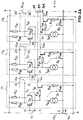
- FIG. 2a which shows a circuit arrangement with three amplifier stages V 1 , V 2 , V 3 as an exemplary embodiment of the amplifier chain from FIG. 1, the amplifier stages V 1 , V 2 , V 3 are differential amplifiers, each with two bipolar amplifier transistors T 10 and T 11 or T 20 and T 21 or T 30 and T 31 , each having an emitter current source Q 1 or Q 2 or Q 3 , in each case a controllable output current source designed as an output transistor T 12 or T 23 or T 32 and in each case two collector resistors R 10 and R 11 or R 20 and R 21 or R 30 and R 31 are formed.
- the base connections of the amplifier transistors T 10 and T 11 or T 20 and T 21 or T 30 and T 31 are each connected to one of the input connections 10 and 11 or 20 and 21 or 30 and 31, the collector connections of the amplifier transistors T 10 and T 11 or T 20 and T 21 or T 30 and T 31 are each connected to one of the output connections 12 and 13 or 22 and 23 or 32 and 33, the output connections 12 or 13 or 22 or 23 or 32 or 33 via the collector resistors R 10 or R 11 or R 20 or R 21 or R 30 or R 31 connected to the first supply connection 1, to which the supply voltage U CC is applied, the emitter connections of the Amplifier transistors T 10 and T 11 or T 20 and T 21 or T 30 and T 31 with the base connection of the output transistor T 12 or T 23 or T 32 and via the emitter current source Q 1 or Q 2 or Q 3 with the second supply connection 2, to which a reference potential is connected, the collector connections of the off gang transistors T 12 or T 23 or T 32 each connected to the measuring output 14 or 24 or 34 and the emitter
- the emitter connections of the Vetttärker transistors T 10 and T 11 or T 20 and T 21 or T 30 and T 31 are advantageously via the base resistors R 12 or R 22 or R 32 to the base connections of the output transistors T 12 or T 23 or T 32 and the emitter connections of the output transistors T 12 , T 22 , T 32 are each connected to the third supply connection 3 via one of the emitter resistors R 13, R 14 and R 15 .
- the emitter current sources Q 1 , Q 2 , Q 3 are each designed as a bipolar transistor or as a field effect transistor, for example as a MOS transistor, which are controlled in such a way that they are proportional to and proportional to the temperature of the amplifier stages V 1 , V 2 , V 3 supply a cross-current I Q1 or I Q2 or I Q3 which is inversely proportional to a given reference resistance .
- the amplification factors of the amplifier stages V 1 , V 2 , V 3 since they are known to be proportional to the respective cross current I Q1 or I Q2 or I Q3 , are proportional to the respective collector resistances R 10 , R 11 or R 20 , R 21 or R 30 , R 31 and inversely proportional to the temperature of the amplifier transistors T 10 , T 11 or T 21 , T 22 or T 31 , T 32 and thus inversely proportional to the temperature of the amplifier stages V 1 or V 2 or V 3 are independent of temperature.
- the measuring currents I M1 or I M2 or I M3 flowing through the measuring outputs 14 or 24 or 34 are determined by the emitter voltages U VE1 or U VE2 or U VE2 of the respective amplifier transistors T 10 , T 11 or T 20 , T 21 or T 30 , T 31 controlled.
- This emitter voltages U VE1 or U VE2 or U VE2 each comprise a DC component and a respective of the alternating component of the respective amplifier stage V 1 and V 2 and V 3 applied voltage U E and U V1, U V2 by rectifying formed rectified portion.
- the measuring currents I M1 or I M2 or I M3 are therefore each composed of a quiescent component and a modulation component.
- the quiescent components are those components of the measuring currents I M1 or I M2 or I M3 that flow when the amplitude of the input signal U E is 0 V.
- the modulation components depend on the modulation of the respective amplifier stage V 1 or V 2 or V 3 , ie on the amplitude of the voltage U E or U V1 or U V2 supplied to the respective amplifier stage V 1 or V 2 or V 3 dependent and they are each at a maximum value for overdriven amplifier stages V 1 , V 2 , V 3 limited.
- the voltages U V1 , U V2 , U V3 supplied by the amplifier stages V 1 , V 2 , V 3 are also temperature-independent, so that with the same amplitude of the input signal U E always the same number of amplifier stages V 1 , V 2 , V 3 are overdriven.
- the maximum value of the measuring currents I M1 , I M2 , I M3 is approximately linearly dependent on the temperature.
- the I Q1, I Q2 and I Q3 dependent on the cross-currents to the emitter terminals of the amplifier transistors T 10, T 11 and T 20, T 21 and T 30, T 31 pending emitter voltages U VE1 and U VE2 or U VE3 , through which the output transistors T 12 or T 22 or T 32 are controlled.
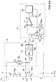
- FIG. 2b which shows an exemplary embodiment of the summation unit S from FIG. 1 and an evaluation unit A as an exemplary embodiment of a circuit arrangement for evaluating the sum signal I S
- the summation unit S has one with the measurement outputs 14, 24, 34 of the amplifier stages V 1 and V 2 or V 3 connected summation node 50, a quiescent current source Q 0 , via which the summation node 50 is connected to the first supply connection 1, and a low-pass filter TP, via which the summation node 50 is connected to the summation output 51 of the summation unit S.
- the output 52 of the low-pass filter TP is designed as a current output, ie the low-pass filter TP has an output current source Q S for decoupling the summation current I S.
- the evaluation unit A comprises the controllable comparison current source Q V , the comparison unit K and the control unit ST.
- the comparison current source Q V is connected to the summation output 51 and to the input 60 of the comparison unit K.
- the comparison current I V of the comparison current source Q V can be reversed by a digital control signal S D supplied by the control unit ST between different reference resistors proportional to the temperature of the amplifier stages V 1 , V 2 , V 3 and to the predetermined reference resistance proportional current values can be switched.
- the comparison current source Q V accordingly acts as a digital-to-analog converter, which generates an analog current - the comparison current I V - with the same temperature coefficient as the summation current I S from the digital control signal S D.
- To control the comparison current I V it has a control input 62, which is connected via the control unit ST to the output 61 of the comparison stage K and to which the digital control signal S D is supplied.
- the comparison current source Q V of the evaluation unit A and the output current source Q S of the low-pass filter TP are designed as bipolar transistors or as field-effect transistors, for example as MOS transistors.
- the measuring currents I M1 , I M2 , I M3 are summed at the summing node 50, their quiescent components being compensated for by a quiescent current I 0 supplied by the quiescent current source Q 0 .
- the low-pass filter TP is therefore only supplied with a sum measurement current I MS composed of the modulation components of the measurement currents I M1 , I M2 , I M3 , which has frequency components originating from the input signal U E.
- the low-pass filter TP generates the summation current I S from the total measurement current I MS by suppressing the frequency components originating from the input signal U E , which due to its dependence on the measurement currents I M1 , I M2 , I M3 is proportional to the temperature of the amplifier stages V 1 , V 2 , V 3 is.
- a temperature-independent voltage U S is set which, depending on whether the summation current I S is greater or less than the comparison current I V, is greater or less than one Threshold voltage U SCH is.
- a temperature-independent evaluation signal U A is therefore present at the output 61 of the comparison stage K, which corresponds to the sign of the difference between the comparison current I V and the summation current I S.
- the comparison current source Q V is controlled by the control unit ST in such a way that the comparison current I V tracks the summation current I S.
- the digital control signal S D is varied, the control unit ST using the evaluation signal U A recognizing in which direction the variation of the digital control signal S D must take place. Because of the temperature independence of the evaluation signal U A , the digital control signal S D is also temperature independent, so that the amplitude of the input signal U E corresponds to the digital control signal S D , ie can be assigned a value corresponding to the digital control signal S D.
Landscapes
- Engineering & Computer Science (AREA)
- Power Engineering (AREA)
- Physics & Mathematics (AREA)
- General Physics & Mathematics (AREA)
- Amplifiers (AREA)
- Measuring Temperature Or Quantity Of Heat (AREA)
Applications Claiming Priority (2)
| Application Number | Priority Date | Filing Date | Title |
|---|---|---|---|
| DE1996124391 DE19624391A1 (de) | 1996-06-19 | 1996-06-19 | Schaltungsanordnung zur Bildung eines der Amplitude eines Eingangssignals entsprechenden Ausgangssignals |
| DE19624391 | 1996-06-19 |
Publications (2)
| Publication Number | Publication Date |
|---|---|
| EP0814341A2 true EP0814341A2 (fr) | 1997-12-29 |
| EP0814341A3 EP0814341A3 (fr) | 1999-04-21 |
Family
ID=7797330
Family Applications (1)
| Application Number | Title | Priority Date | Filing Date |
|---|---|---|---|
| EP97109102A Withdrawn EP0814341A3 (fr) | 1996-06-19 | 1997-06-05 | Circuit pour établir un signal de sortie correspondant à l'amplitude d'un signal d'entrée |
Country Status (2)
| Country | Link |
|---|---|
| EP (1) | EP0814341A3 (fr) |
| DE (1) | DE19624391A1 (fr) |
Families Citing this family (1)
| Publication number | Priority date | Publication date | Assignee | Title |
|---|---|---|---|---|
| JP4343060B2 (ja) | 2004-08-26 | 2009-10-14 | シャープ株式会社 | 受信信号強度測定回路、受信信号強度検出回路および無線受信機 |
Family Cites Families (5)
| Publication number | Priority date | Publication date | Assignee | Title |
|---|---|---|---|---|
| DE2545535C3 (de) * | 1975-10-10 | 1979-02-22 | Rohde & Schwarz, 8000 Muenchen | Schaltung zum Erzeugen einer dem Logarithmus einer Eingangswechselspannung entsprechenden Ausgangsgleichspannung |
| US4442549A (en) * | 1982-05-27 | 1984-04-10 | Motorola, Inc. | Meter drive circuit |
| US4794342A (en) * | 1986-06-04 | 1988-12-27 | Nec Corporation | Intermediate frequency amplification circuit capable of detecting a field strength with low electric power |
| EP0517305B1 (fr) * | 1991-06-03 | 1995-11-22 | Koninklijke Philips Electronics N.V. | Amplificateur et détecteur logarithmique |
| US5298811A (en) * | 1992-08-03 | 1994-03-29 | Analog Devices, Inc. | Synchronous logarithmic amplifier |
-
1996
- 1996-06-19 DE DE1996124391 patent/DE19624391A1/de not_active Withdrawn
-
1997
- 1997-06-05 EP EP97109102A patent/EP0814341A3/fr not_active Withdrawn
Also Published As
| Publication number | Publication date |
|---|---|
| DE19624391A1 (de) | 1998-01-02 |
| EP0814341A3 (fr) | 1999-04-21 |
Similar Documents
| Publication | Publication Date | Title |
|---|---|---|
| DE69528234T2 (de) | Schaltung und Verfahren zur Erzeugung eines Taktsignals | |
| DE3872275T2 (de) | Cmos-referenzspannungsgeneratoreinrichtung. | |
| DE3878069T2 (de) | Breitbandverstaerker. | |
| DE68903243T2 (de) | Spannungs-stromumsetzer mit mos-transistoren. | |
| DE19837153A1 (de) | Pulsweitenmodulierter Gleichspannungswandler | |
| EP0365085B1 (fr) | Circuit de commande de l'amplitude d'un signal | |
| DE102009033414B4 (de) | Integrierter Schaltkreis mit einpoligem Eingang und differenziellem Ausgang, Verfahren und elektronische Vorrichtung | |
| EP0460263B1 (fr) | Etage de sortie linéaire réalisé en technologie CMOS | |
| EP0217223B1 (fr) | Convertisseur numérique-analogique à compensation de température | |
| DE69130124T2 (de) | Logarithmischer Verstärker | |
| DE2702022B2 (de) | Verstärkerschaltung | |
| DE69514417T2 (de) | Differenzverstärker | |
| EP0744828B1 (fr) | Circuit amplificateur à transimpédance | |
| CH684855A5 (de) | MOSFET-Analogvervielfacher. | |
| DE3336949C2 (de) | Pufferverstärker | |
| DE2852567A1 (de) | Verstaerker mit einem ersten und einem zweiten verstaerkerelement | |
| DE102021132633A1 (de) | Verfahren und Schaltung zur Stromerfassung | |
| DE4109893A1 (de) | Integrierte schaltungsanordnung mit einem differenzverstaerker | |
| DE102004022991B3 (de) | Abtast-Differenzverstärker und Abtast-Verstärker | |
| EP0814341A2 (fr) | Circuit pour établir un signal de sortie correspondant à l'amplitude d'un signal d'entrée | |
| DE60133068T2 (de) | Differentiell angeordnetes transistorpaar mit mitteln zur degeneration der transkonduktanz | |
| EP0133618A1 (fr) | Circuit oscillateur haute fréquence à quartz sous forme de circuit intégré monolithique | |
| DE3228785C2 (fr) | ||
| EP0277377A1 (fr) | Circuit à limitation de courant | |
| DE3724980A1 (de) | Spannungswiederholerschaltung fuer eine ohmsche komponente aufweisende last mit kompensation der oberwellenverzerrung |
Legal Events
| Date | Code | Title | Description |
|---|---|---|---|
| PUAI | Public reference made under article 153(3) epc to a published international application that has entered the european phase |
Free format text: ORIGINAL CODE: 0009012 |
|
| AK | Designated contracting states |
Kind code of ref document: A2 Designated state(s): DE FR GB IT |
|
| RAP1 | Party data changed (applicant data changed or rights of an application transferred) |
Owner name: TEMIC SEMICONDUCTOR GMBH |
|
| PUAL | Search report despatched |
Free format text: ORIGINAL CODE: 0009013 |
|
| AK | Designated contracting states |
Kind code of ref document: A3 Designated state(s): AT BE CH DE DK ES FI FR GB GR IE IT LI LU MC NL PT SE |
|
| 17P | Request for examination filed |
Effective date: 19990925 |
|
| AKX | Designation fees paid |
Free format text: DE FR GB IT |
|
| STAA | Information on the status of an ep patent application or granted ep patent |
Free format text: STATUS: THE APPLICATION HAS BEEN WITHDRAWN |
|
| 18W | Application withdrawn |
Withdrawal date: 20000222 |