EP0814510A2 - Filmträger und in einer Halbleiteranordnung verwendete Filmträger - Google Patents
Filmträger und in einer Halbleiteranordnung verwendete Filmträger Download PDFInfo
- Publication number
- EP0814510A2 EP0814510A2 EP97110042A EP97110042A EP0814510A2 EP 0814510 A2 EP0814510 A2 EP 0814510A2 EP 97110042 A EP97110042 A EP 97110042A EP 97110042 A EP97110042 A EP 97110042A EP 0814510 A2 EP0814510 A2 EP 0814510A2
- Authority
- EP
- European Patent Office
- Prior art keywords
- patterns
- dummy
- semiconductor device
- tape
- metallic
- Prior art date
- Legal status (The legal status is an assumption and is not a legal conclusion. Google has not performed a legal analysis and makes no representation as to the accuracy of the status listed.)
- Granted
Links
Images

Classifications
-
- H—ELECTRICITY
- H10—SEMICONDUCTOR DEVICES; ELECTRIC SOLID-STATE DEVICES NOT OTHERWISE PROVIDED FOR
- H10W—GENERIC PACKAGES, INTERCONNECTIONS, CONNECTORS OR OTHER CONSTRUCTIONAL DETAILS OF DEVICES COVERED BY CLASS H10
- H10W72/00—Interconnections or connectors in packages
- H10W72/071—Connecting or disconnecting
-
- H—ELECTRICITY
- H10—SEMICONDUCTOR DEVICES; ELECTRIC SOLID-STATE DEVICES NOT OTHERWISE PROVIDED FOR
- H10W—GENERIC PACKAGES, INTERCONNECTIONS, CONNECTORS OR OTHER CONSTRUCTIONAL DETAILS OF DEVICES COVERED BY CLASS H10
- H10W72/00—Interconnections or connectors in packages
- H10W72/90—Bond pads, in general
-
- H—ELECTRICITY
- H05—ELECTRIC TECHNIQUES NOT OTHERWISE PROVIDED FOR
- H05K—PRINTED CIRCUITS; CASINGS OR CONSTRUCTIONAL DETAILS OF ELECTRIC APPARATUS; MANUFACTURE OF ASSEMBLAGES OF ELECTRICAL COMPONENTS
- H05K3/00—Apparatus or processes for manufacturing printed circuits
- H05K3/30—Assembling printed circuits with electric components, e.g. with resistors
- H05K3/32—Assembling printed circuits with electric components, e.g. with resistors electrically connecting electric components or wires to printed circuits
- H05K3/34—Assembling printed circuits with electric components, e.g. with resistors electrically connecting electric components or wires to printed circuits by soldering
- H05K3/3452—Solder masks
-
- H—ELECTRICITY
- H10—SEMICONDUCTOR DEVICES; ELECTRIC SOLID-STATE DEVICES NOT OTHERWISE PROVIDED FOR
- H10W—GENERIC PACKAGES, INTERCONNECTIONS, CONNECTORS OR OTHER CONSTRUCTIONAL DETAILS OF DEVICES COVERED BY CLASS H10
- H10W70/00—Package substrates; Interposers; Redistribution layers [RDL]
- H10W70/40—Leadframes
- H10W70/453—Leadframes comprising flexible metallic tapes
-
- H—ELECTRICITY
- H10—SEMICONDUCTOR DEVICES; ELECTRIC SOLID-STATE DEVICES NOT OTHERWISE PROVIDED FOR
- H10W—GENERIC PACKAGES, INTERCONNECTIONS, CONNECTORS OR OTHER CONSTRUCTIONAL DETAILS OF DEVICES COVERED BY CLASS H10
- H10W70/00—Package substrates; Interposers; Redistribution layers [RDL]
- H10W70/60—Insulating or insulated package substrates; Interposers; Redistribution layers
- H10W70/67—Insulating or insulated package substrates; Interposers; Redistribution layers characterised by their insulating layers or insulating parts
- H10W70/688—Flexible insulating substrates
-
- H—ELECTRICITY
- H05—ELECTRIC TECHNIQUES NOT OTHERWISE PROVIDED FOR
- H05K—PRINTED CIRCUITS; CASINGS OR CONSTRUCTIONAL DETAILS OF ELECTRIC APPARATUS; MANUFACTURE OF ASSEMBLAGES OF ELECTRICAL COMPONENTS
- H05K1/00—Printed circuits
- H05K1/02—Details
- H05K1/03—Use of materials for the substrate
- H05K1/0393—Flexible materials
-
- H—ELECTRICITY
- H05—ELECTRIC TECHNIQUES NOT OTHERWISE PROVIDED FOR
- H05K—PRINTED CIRCUITS; CASINGS OR CONSTRUCTIONAL DETAILS OF ELECTRIC APPARATUS; MANUFACTURE OF ASSEMBLAGES OF ELECTRICAL COMPONENTS
- H05K2201/00—Indexing scheme relating to printed circuits covered by H05K1/00
- H05K2201/09—Shape and layout
- H05K2201/09209—Shape and layout details of conductors
- H05K2201/09654—Shape and layout details of conductors covering at least two types of conductors provided for in H05K2201/09218 - H05K2201/095
- H05K2201/09781—Dummy conductors, i.e. not used for normal transport of current; Dummy electrodes of components
-
- H—ELECTRICITY
- H05—ELECTRIC TECHNIQUES NOT OTHERWISE PROVIDED FOR
- H05K—PRINTED CIRCUITS; CASINGS OR CONSTRUCTIONAL DETAILS OF ELECTRIC APPARATUS; MANUFACTURE OF ASSEMBLAGES OF ELECTRICAL COMPONENTS
- H05K2201/00—Indexing scheme relating to printed circuits covered by H05K1/00
- H05K2201/10—Details of components or other objects attached to or integrated in a printed circuit board
- H05K2201/10613—Details of electrical connections of non-printed components, e.g. special leads
- H05K2201/10621—Components characterised by their electrical contacts
- H05K2201/10681—Tape Carrier Package [TCP]; Flexible sheet connector
-
- H—ELECTRICITY
- H10—SEMICONDUCTOR DEVICES; ELECTRIC SOLID-STATE DEVICES NOT OTHERWISE PROVIDED FOR
- H10W—GENERIC PACKAGES, INTERCONNECTIONS, CONNECTORS OR OTHER CONSTRUCTIONAL DETAILS OF DEVICES COVERED BY CLASS H10
- H10W70/00—Package substrates; Interposers; Redistribution layers [RDL]
- H10W70/60—Insulating or insulated package substrates; Interposers; Redistribution layers
- H10W70/62—Insulating or insulated package substrates; Interposers; Redistribution layers characterised by their interconnections
- H10W70/65—Shapes or dispositions of interconnections
- H10W70/654—Top-view layouts
- H10W70/655—Fan-out layouts
-
- H—ELECTRICITY
- H10—SEMICONDUCTOR DEVICES; ELECTRIC SOLID-STATE DEVICES NOT OTHERWISE PROVIDED FOR
- H10W—GENERIC PACKAGES, INTERCONNECTIONS, CONNECTORS OR OTHER CONSTRUCTIONAL DETAILS OF DEVICES COVERED BY CLASS H10
- H10W72/00—Interconnections or connectors in packages
- H10W72/20—Bump connectors, e.g. solder bumps or copper pillars; Dummy bumps; Thermal bumps
-
- H—ELECTRICITY
- H10—SEMICONDUCTOR DEVICES; ELECTRIC SOLID-STATE DEVICES NOT OTHERWISE PROVIDED FOR
- H10W—GENERIC PACKAGES, INTERCONNECTIONS, CONNECTORS OR OTHER CONSTRUCTIONAL DETAILS OF DEVICES COVERED BY CLASS H10
- H10W72/00—Interconnections or connectors in packages
- H10W72/20—Bump connectors, e.g. solder bumps or copper pillars; Dummy bumps; Thermal bumps
- H10W72/29—Bond pads specially adapted therefor
Definitions
- This invention relates to a TAB tape and a semiconductor device using the TAB tape, and more particularly to a TAB tape used as a tape-type Ball Grid Array (BGA).
- BGA Ball Grid Array
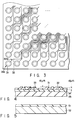
- FIG. 3 is a plan view, showing a conventional TAB tape of a three-layer structure.
- FIG. 4 is a cross sectional view, showing the TAB tape of FIG. 3.
- the TAB tape shown in FIGS. 3 and 4 comprises a resin tape 35 made of polyimide, an adhesive 34 coated on the resin tape, and copper foil patterns 31 and 32 formed on the adhesive.
- the copper foil patterns 31 and 32 consist of pads 31a to which solder balls are adhered, and leads 32a for connecting the pads 31a to a semiconductor chip (not shown).
- the copper foil patterns 31 and 32, the exposed portions of the adhesive 34 are coated with solder resist 33 which protects them. A hole is formed in the portion of the solder resist 33 which is located on each pad 31a.
- each copper foil pattern has a film thickness of 18 ⁇ m
- the difference in level is also 18 ⁇ m between the upper surface of each of the portions of the solder resist 35 which are coated on the copper foil patterns 31 and 32, and the upper surface of each of the portions of the solder resist 33 which are coated on the exposed portions of the adhesive 34.
- FIG. 5 shows a stiffener, to which the polyimide tape 35 of the TAB tape is adhered.
- This stiffener is for a BGA tape, and comprises a metal plate 52 and an adhesive 51 coated thereon.
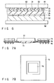
- FIG. 6 is a view, useful in explaining a process for adhering the TAB tape shown in FIG. 4 to the stiffener shown in FIG. 5 by thermo-compression bonding.
- elements similar to those shown in FIGS. 4 and 5 are denoted by corresponding reference numerals, and no explanation is given thereof.
- the TAB tape and the stiffener are held between tools 61 and 62. In this state, pressure is applied to the TAB tape and the stiffener from the outside of both the tools 61 and 62, while heat is applied thereto. As a result, the tape and the stiffener are adhered to each other by means of the adhesive 51.
- FIG. 7A is a plan view of the semiconductor device shown in FIG. 7A.
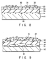
- the solder resist 33 has great irregularities as described above, and therefore the pressure from the upper and lower tools 61 and 62 does not reach the deep concave portions 63 of the solder resist. Accordingly, the adhesive 51 are not sufficiently pressed at locations below the concave portions 63, and hence may well have an insufficiently adhered portion 81 as shown in FIG 8.
- FIG. 9 is a sectional view, showing the state of the BGA tape in which a babble 91 occurs therein. As is understood from FIG. 9, the BGA tape is warped due to the babble 91, thereby degrading the flatness of a package, and it is difficult to make the lights the solder balls equal.
- the invention comprises a resin tape, pads formed on the resin tape, copper foil patterns constituting leads, dummy copper foil patterns provided between the copper foil patterns, and solder resist coated on the overall surfaces of the copper foil patterns and the dummy copper foil patterns.
- FIG. 1 is a sectional view, showing a BGA tape according to the embodiment of the invention.
- FIG. 2 is a plan view of the embodiment of FIG. 1. The sectional view of FIG. 1 is taken along lines I - I of FIG. 2.
- an adhesive 14 is coated on one surface of a resin tape 15 made, for example, of polyimide.
- Metallic patterns, for example, copper foil patterns 19 are formed on the adhesive 14.
- the copper foil patterns 19 consists of pads 11 to which solder balls are attached, and leads 12 for connecting the pads 11 to a semiconductor chip.
- Each lead 12 has a width of e.g. 30 - 60 ⁇ m.
- the adhesive 14 is provided with dummy metallic patterns 10, 10a, 10b such as copper foil patterns 19.
- the dummy metallic pattern means a pattern electrically connected between the pad 11 and the lead 12, and having a width greater than the lead 12, or a pattern electrically connected neither to the pad 11 nor to the lead 12.
- the width of the pattern is, for example, 600 - 800 ⁇ m at maximum.
- the copper foil patterns 10 - 12 are coated with solder resist 13.
- the opposite side of the polyimide tape 15 is adhered to a metal plate 17 by means of an adhesive 16.
- the metal plate 17 and the adhesive 16 are constitute a stiffener.
- each of dummy patterns 10, 10a, 10b is formed in a wide space defined between adjacent ones of the pads 11 or of the leads 12, or between each pad 11 and a corresponding lead 12.
- the dummy patterns 10 are formed simultaneous with the pads 11 and the lead 12.
- the dummy pattern may be formed independent of the other elements as dummy patterns 10, 10a, or connected to the pad 11 as a dummy pattern 10b, or grounded.
- the areas of the portions of the adhesive 14 which are exposed in a stage before the coating of the solder resist 13 are minimized by providing the dummy patterns 10, 10a, 10b on the adhesive 14. Since the solder resist 13 is applied in this stage, the difference in level is minimized between the upper surface of each of the portions of the solder resist 13 which are coated on the copper foil patterns 19, and the upper surface of each of the portions of the solder resist 13 which are coated on the exposed portions of the adhesive 14. If the film thickness of the copper foil patterns 19 is 18 ⁇ m, the difference in level can be reduced to 3 - 18 ⁇ m, more particularly to 7 ⁇ m or less.
- the contact area between the adhesive 14 and the copper foil patterns is increased by connecting dummy patterns to leads and pads, the strength of adhesion between the TAB tape 15 and the copper foil is increased.
- grounding the dummy patterns formed between the pads will reduce the inductance between each pair of adjacent pads.
- the TAB tape has a three-layer structure
- the invention is not limited to this.
- the TAB tape may have a double layer structure consisting of a resin tape and a copper foil pattern layer.
- the patterns and the dummy patterns are not limited to copper foil patterns.
Landscapes
- Engineering & Computer Science (AREA)
- Manufacturing & Machinery (AREA)
- Microelectronics & Electronic Packaging (AREA)
- Wire Bonding (AREA)
Applications Claiming Priority (2)
| Application Number | Priority Date | Filing Date | Title |
|---|---|---|---|
| JP15968696A JP3346985B2 (ja) | 1996-06-20 | 1996-06-20 | 半導体装置 |
| JP159686/96 | 1996-06-20 |
Publications (3)
| Publication Number | Publication Date |
|---|---|
| EP0814510A2 true EP0814510A2 (de) | 1997-12-29 |
| EP0814510A3 EP0814510A3 (de) | 1999-04-21 |
| EP0814510B1 EP0814510B1 (de) | 2006-06-21 |
Family
ID=15699111
Family Applications (1)
| Application Number | Title | Priority Date | Filing Date |
|---|---|---|---|
| EP97110042A Expired - Lifetime EP0814510B1 (de) | 1996-06-20 | 1997-06-19 | Filmträger und in einer Halbleiteranordnung verwendete Filmträger |
Country Status (7)
| Country | Link |
|---|---|
| US (1) | US5892277A (de) |
| EP (1) | EP0814510B1 (de) |
| JP (1) | JP3346985B2 (de) |
| KR (1) | KR100253872B1 (de) |
| CN (1) | CN1087102C (de) |
| DE (1) | DE69736157T2 (de) |
| TW (1) | TW460996B (de) |
Cited By (2)
| Publication number | Priority date | Publication date | Assignee | Title |
|---|---|---|---|---|
| US6528417B1 (en) * | 2001-09-17 | 2003-03-04 | Taiwan Semiconductor Manufacturing Company | Metal patterned structure for SiN surface adhesion enhancement |
| US6909053B2 (en) * | 2001-10-02 | 2005-06-21 | Nec Lcd Technologies, Ltd. | Circuit substrate connecting structure, liquid crystal display device having the connecting structure and mounting method of liquid crystal display device |
Families Citing this family (15)
| Publication number | Priority date | Publication date | Assignee | Title |
|---|---|---|---|---|
| JP3638778B2 (ja) * | 1997-03-31 | 2005-04-13 | 株式会社ルネサステクノロジ | 半導体集積回路装置およびその製造方法 |
| US6194313B1 (en) * | 1997-04-30 | 2001-02-27 | Texas Instruments Incorporated | Method for reducing recess for the formation of local interconnect and or plug trench fill for etchback process |
| JP4307664B2 (ja) * | 1999-12-03 | 2009-08-05 | 株式会社ルネサステクノロジ | 半導体装置 |
| TW469552B (en) * | 1999-12-10 | 2001-12-21 | Toshiba Corp | TAB type semiconductor device |
| US6501170B1 (en) | 2000-06-09 | 2002-12-31 | Micron Technology, Inc. | Substrates and assemblies including pre-applied adhesion promoter |
| US6555910B1 (en) * | 2000-08-29 | 2003-04-29 | Agere Systems Inc. | Use of small openings in large topography features to improve dielectric thickness control and a method of manufacture thereof |
| KR100378185B1 (ko) * | 2000-10-16 | 2003-03-29 | 삼성전자주식회사 | 테스트용 탭을 구비하는 마이크로 비지에이 패키지 테이프 |
| JP4626919B2 (ja) * | 2001-03-27 | 2011-02-09 | ルネサスエレクトロニクス株式会社 | 半導体装置 |
| JP2009527121A (ja) * | 2006-02-15 | 2009-07-23 | エヌエックスピー ビー ヴィ | 半導体パッケージの製造方法、パッケージ基板、および集積回路(ic)デバイス |
| TWI474458B (zh) * | 2012-03-23 | 2015-02-21 | Chipmos Technologies Inc | 半導體封裝基板 |
| US9275967B2 (en) | 2014-01-06 | 2016-03-01 | Taiwan Semiconductor Manufacturing Company, Ltd. | Protrusion bump pads for bond-on-trace processing |
| US9418928B2 (en) | 2014-01-06 | 2016-08-16 | Taiwan Semiconductor Manufacturing Company, Ltd. | Protrusion bump pads for bond-on-trace processing |
| US9508637B2 (en) | 2014-01-06 | 2016-11-29 | Taiwan Semiconductor Manufacturing Company, Ltd. | Protrusion bump pads for bond-on-trace processing |
| US9305890B2 (en) | 2014-01-15 | 2016-04-05 | Taiwan Semiconductor Manufacturing Company, Ltd. | Package having substrate with embedded metal trace overlapped by landing pad |
| KR102214512B1 (ko) * | 2014-07-04 | 2021-02-09 | 삼성전자 주식회사 | 인쇄회로기판 및 이를 이용한 반도체 패키지 |
Family Cites Families (8)
| Publication number | Priority date | Publication date | Assignee | Title |
|---|---|---|---|---|
| US5162896A (en) * | 1987-06-02 | 1992-11-10 | Kabushiki Kaisha Toshiba | IC package for high-speed semiconductor integrated circuit device |
| US4916514A (en) * | 1988-05-31 | 1990-04-10 | Unisys Corporation | Integrated circuit employing dummy conductors for planarity |
| JP2864705B2 (ja) * | 1990-09-21 | 1999-03-08 | セイコーエプソン株式会社 | Tab用フイルムキャリアテープ及びそのリードへのはんだ被覆方法 |
| JPH081917B2 (ja) * | 1991-01-22 | 1996-01-10 | 株式会社東芝 | フィルムキャリアテ−プ |
| JP3197291B2 (ja) * | 1991-04-30 | 2001-08-13 | 株式会社リコー | Tab実装体 |
| US5289032A (en) * | 1991-08-16 | 1994-02-22 | Motorola, Inc. | Tape automated bonding(tab)semiconductor device and method for making the same |
| US5441915A (en) * | 1992-09-01 | 1995-08-15 | Taiwan Semiconductor Manufacturing Company Ltd. | Process of fabrication planarized metallurgy structure for a semiconductor device |
| JPH088295A (ja) * | 1994-06-20 | 1996-01-12 | Toshiba Corp | 半導体実装装置およびその製造方法 |
-
1996
- 1996-06-20 JP JP15968696A patent/JP3346985B2/ja not_active Expired - Fee Related
-
1997
- 1997-06-12 TW TW086108122A patent/TW460996B/zh not_active IP Right Cessation
- 1997-06-19 DE DE69736157T patent/DE69736157T2/de not_active Expired - Lifetime
- 1997-06-19 EP EP97110042A patent/EP0814510B1/de not_active Expired - Lifetime
- 1997-06-19 US US08/879,304 patent/US5892277A/en not_active Expired - Fee Related
- 1997-06-20 CN CN97113834A patent/CN1087102C/zh not_active Expired - Fee Related
- 1997-06-20 KR KR1019970026004A patent/KR100253872B1/ko not_active Expired - Fee Related
Cited By (2)
| Publication number | Priority date | Publication date | Assignee | Title |
|---|---|---|---|---|
| US6528417B1 (en) * | 2001-09-17 | 2003-03-04 | Taiwan Semiconductor Manufacturing Company | Metal patterned structure for SiN surface adhesion enhancement |
| US6909053B2 (en) * | 2001-10-02 | 2005-06-21 | Nec Lcd Technologies, Ltd. | Circuit substrate connecting structure, liquid crystal display device having the connecting structure and mounting method of liquid crystal display device |
Also Published As
| Publication number | Publication date |
|---|---|
| KR100253872B1 (ko) | 2000-04-15 |
| DE69736157T2 (de) | 2007-05-03 |
| TW460996B (en) | 2001-10-21 |
| EP0814510A3 (de) | 1999-04-21 |
| CN1170234A (zh) | 1998-01-14 |
| EP0814510B1 (de) | 2006-06-21 |
| US5892277A (en) | 1999-04-06 |
| CN1087102C (zh) | 2002-07-03 |
| JP3346985B2 (ja) | 2002-11-18 |
| KR980005944A (ko) | 1998-03-30 |
| JPH1012676A (ja) | 1998-01-16 |
| DE69736157D1 (de) | 2006-08-03 |
Similar Documents
| Publication | Publication Date | Title |
|---|---|---|
| US5892277A (en) | Tab tape and semiconductor device using the tab tape | |
| US5367435A (en) | Electronic package structure and method of making same | |
| KR100537972B1 (ko) | 집적 회로 패키지용 칩 스케일 볼 그리드 어레이 | |
| US6985362B2 (en) | Printed circuit board and electronic package using same | |
| US5329423A (en) | Compressive bump-and-socket interconnection scheme for integrated circuits | |
| US5414299A (en) | Semi-conductor device interconnect package assembly for improved package performance | |
| EP0948814B1 (de) | Lötballgitter in chipgrösse für integrierte schaltungspackung | |
| US6329605B1 (en) | Components with conductive solder mask layers | |
| EP0907204A2 (de) | Halbleitervorrichtung in Chip-Grösse und Verfahren zu deren Herstellung | |
| JP2768650B2 (ja) | ソルダーボールの装着溝を有する印刷回路基板とこれを使用したボールグリッドアレイパッケージ | |
| EP0724290A2 (de) | Elektronische Packung | |
| KR20010072583A (ko) | 적층화 집적 회로 패키지 | |
| US5731636A (en) | Semiconductor bonding package | |
| JP2000332055A (ja) | フリップチップ実装構造及び実装方法 | |
| JP2004128337A (ja) | Cof半導体装置およびその製造方法 | |
| US20020096750A1 (en) | Package for semiconductor chip having thin recess portion and thick plane portion | |
| JP2753696B2 (ja) | 半導体パッケージのテープ自動結合構造 | |
| JPH0745641A (ja) | 半導体装置の実装方法 | |
| US6192579B1 (en) | Tape carrier and manufacturing method therefor | |
| US6818542B2 (en) | Tape circuit board and semiconductor chip package including the same | |
| US6504239B1 (en) | Semiconductor device having dummy pattern that relieves stress | |
| JP3018789B2 (ja) | 半導体装置 | |
| JPH07111379A (ja) | マルチチップモジュール実装型プリント配線板 | |
| JP3646056B2 (ja) | フリップチップ実装方法 | |
| US6755229B2 (en) | Method for preparing high performance ball grid array board and jig applicable to said method |
Legal Events
| Date | Code | Title | Description |
|---|---|---|---|
| PUAI | Public reference made under article 153(3) epc to a published international application that has entered the european phase |
Free format text: ORIGINAL CODE: 0009012 |
|
| 17P | Request for examination filed |
Effective date: 19970710 |
|
| AK | Designated contracting states |
Kind code of ref document: A2 Designated state(s): DE FR GB |
|
| PUAL | Search report despatched |
Free format text: ORIGINAL CODE: 0009013 |
|
| AK | Designated contracting states |
Kind code of ref document: A3 Designated state(s): AT BE CH DE DK ES FI FR GB GR IE IT LI LU MC NL PT SE |
|
| AKX | Designation fees paid |
Free format text: DE FR GB |
|
| 17Q | First examination report despatched |
Effective date: 20030808 |
|
| GRAP | Despatch of communication of intention to grant a patent |
Free format text: ORIGINAL CODE: EPIDOSNIGR1 |
|
| GRAS | Grant fee paid |
Free format text: ORIGINAL CODE: EPIDOSNIGR3 |
|
| GRAA | (expected) grant |
Free format text: ORIGINAL CODE: 0009210 |
|
| AK | Designated contracting states |
Kind code of ref document: B1 Designated state(s): DE FR GB |
|
| REG | Reference to a national code |
Ref country code: GB Ref legal event code: FG4D |
|
| REF | Corresponds to: |
Ref document number: 69736157 Country of ref document: DE Date of ref document: 20060803 Kind code of ref document: P |
|
| ET | Fr: translation filed | ||
| PLBE | No opposition filed within time limit |
Free format text: ORIGINAL CODE: 0009261 |
|
| STAA | Information on the status of an ep patent application or granted ep patent |
Free format text: STATUS: NO OPPOSITION FILED WITHIN TIME LIMIT |
|
| 26N | No opposition filed |
Effective date: 20070322 |
|
| PGFP | Annual fee paid to national office [announced via postgrant information from national office to epo] |
Ref country code: FR Payment date: 20100709 Year of fee payment: 14 |
|
| PGFP | Annual fee paid to national office [announced via postgrant information from national office to epo] |
Ref country code: GB Payment date: 20100616 Year of fee payment: 14 Ref country code: DE Payment date: 20100616 Year of fee payment: 14 |
|
| GBPC | Gb: european patent ceased through non-payment of renewal fee |
Effective date: 20110619 |
|
| REG | Reference to a national code |
Ref country code: FR Ref legal event code: ST Effective date: 20120229 |
|
| REG | Reference to a national code |
Ref country code: DE Ref legal event code: R119 Ref document number: 69736157 Country of ref document: DE Effective date: 20120103 |
|
| PG25 | Lapsed in a contracting state [announced via postgrant information from national office to epo] |
Ref country code: DE Free format text: LAPSE BECAUSE OF NON-PAYMENT OF DUE FEES Effective date: 20120103 Ref country code: FR Free format text: LAPSE BECAUSE OF NON-PAYMENT OF DUE FEES Effective date: 20110630 |
|
| PG25 | Lapsed in a contracting state [announced via postgrant information from national office to epo] |
Ref country code: GB Free format text: LAPSE BECAUSE OF NON-PAYMENT OF DUE FEES Effective date: 20110619 |