EP0815549B1 - Kanalplatte für eine flache anzeigevorrichtung und verfahren zur herstellung einer solchen platte - Google Patents
Kanalplatte für eine flache anzeigevorrichtung und verfahren zur herstellung einer solchen platte Download PDFInfo
- Publication number
- EP0815549B1 EP0815549B1 EP96940074A EP96940074A EP0815549B1 EP 0815549 B1 EP0815549 B1 EP 0815549B1 EP 96940074 A EP96940074 A EP 96940074A EP 96940074 A EP96940074 A EP 96940074A EP 0815549 B1 EP0815549 B1 EP 0815549B1
- Authority
- EP
- European Patent Office
- Prior art keywords
- substrate
- spacer plate
- dielectric sheet
- plate
- channel
- Prior art date
- Legal status (The legal status is an assumption and is not a legal conclusion. Google has not performed a legal analysis and makes no representation as to the accuracy of the status listed.)
- Expired - Lifetime
Links
Images

Classifications
-
- G—PHYSICS
- G09—EDUCATION; CRYPTOGRAPHY; DISPLAY; ADVERTISING; SEALS
- G09F—DISPLAYING; ADVERTISING; SIGNS; LABELS OR NAME-PLATES; SEALS
- G09F9/00—Indicating arrangements for variable information in which the information is built-up on a support by selection or combination of individual elements
- G09F9/30—Indicating arrangements for variable information in which the information is built-up on a support by selection or combination of individual elements in which the desired character or characters are formed by combining individual elements
- G09F9/35—Indicating arrangements for variable information in which the information is built-up on a support by selection or combination of individual elements in which the desired character or characters are formed by combining individual elements being liquid crystals
-
- G—PHYSICS
- G02—OPTICS
- G02F—OPTICAL DEVICES OR ARRANGEMENTS FOR THE CONTROL OF LIGHT BY MODIFICATION OF THE OPTICAL PROPERTIES OF THE MEDIA OF THE ELEMENTS INVOLVED THEREIN; NON-LINEAR OPTICS; FREQUENCY-CHANGING OF LIGHT; OPTICAL LOGIC ELEMENTS; OPTICAL ANALOGUE/DIGITAL CONVERTERS
- G02F1/00—Devices or arrangements for the control of the intensity, colour, phase, polarisation or direction of light arriving from an independent light source, e.g. switching, gating or modulating; Non-linear optics
- G02F1/01—Devices or arrangements for the control of the intensity, colour, phase, polarisation or direction of light arriving from an independent light source, e.g. switching, gating or modulating; Non-linear optics for the control of the intensity, phase, polarisation or colour
- G02F1/13—Devices or arrangements for the control of the intensity, colour, phase, polarisation or direction of light arriving from an independent light source, e.g. switching, gating or modulating; Non-linear optics for the control of the intensity, phase, polarisation or colour based on liquid crystals, e.g. single liquid crystal display cells
- G02F1/133—Constructional arrangements; Operation of liquid crystal cells; Circuit arrangements
- G02F1/1333—Constructional arrangements; Manufacturing methods
- G02F1/13334—Plasma addressed liquid crystal cells [PALC]
Definitions
- PALC devices comprise, typically, a sandwich of: a first substrate having deposited on it parallel transparent column electrodes, commonly referred to as "ITO" columns or electrodes since indium-tin oxides are typically used, on which is deposited a color filter layer; a second substrate comprising parallel sealed plasma channels corresponding to rows of the display crossing all of the ITO columns and each of which is filled with a low pressure ionizable gas, such as helium, neon and/or argon, and containing spaced cathode and anode electrodes along the channel for ionizing the gas to create a plasma, which channels are closed off by a thin transparent dielectric sheet; and a liquid crystal (LC) material located between the substrates.
- a low pressure ionizable gas such as helium, neon and/or argon
- the structure behaves like an active matrix liquid crystal display in which the thin film transistor switches at each pixel are replaced by a plasma channel acting as a row switch and capable of selectively addressing a row of LC pixel elements.
- a plasma channel acting as a row switch and capable of selectively addressing a row of LC pixel elements.
- successive lines of data signals representing an image to be displayed are sampled at column positions and the sampled data voltages are respectively applied to the ITO columns. All but one of the row plasma channels are in the de-ionized or non-conducting state.
- the plasma of the one ionized selected channel is conducting and, in effect, establishes a reference potential on the adjacent side of a row of pixels of the LC layer, causing each LC pixel to charge up to the applied column potential of the data signal.
- the ionized channel is turned off, isolating the LC pixel charge and storing the data voltage for a frame period.
- the next row of data appears on the ITO columns, only the succeeding plasma channel row is ionized to store the data voltages in the succeeding row of LC pixels, and so on.
- the attenuation of the backlight or incident light to each LC pixel is a function of the stored voltage across the pixel. A more detailed description is unnecessary because the construction, fabrication, and operation of such PALC devices have been described in detail in the following U.S.
- FIG. 2 A partial perspective view of the PALC display described in the 1993 SID Digest is shown in Fig. 2.
- the method described in the referenced publication for making the plasma channels is to chemically etch a flat glass substrate to form parallel semi-cylindrically shaped recesses defined by spaced ridges or mesas and to bond on top of the mesas a thin dielectric cover sheet having a thickness in the range of about 30-50 ⁇ m.
- European Patent 0 500 084 A2 describes the formation of channels by patterning of electrodes on a flat substrate, providing spacers on the flat substrate, and placing the thin glass sheet on top of the spacers.
- the discharge space thus extends continuously across the electrodes.
- the continuous discharge space will lead between channels to crosstalk which is difficult to avoid.
- the spacers have to be formed on the flat substrate by deposition and/or etching processes, such as screen printing. Since the spacers have to be as thick as the required channel depth ( ⁇ 100 microns or more) the fabrication of the spacers adds complexity to the process.
- European Patents 0 500 085 A2 and 0554 851 A1 describe the formation of channels by screen printing partition walls. However, this is also a difficult process, which may require multiple coats to obtain the required wall height.
- An object of the invention is an improved channel plate.
- a further object of the invention is an improved plasma-addressed display device.
- Another object of the invention is an improved method for fabricating the plasma channels of a PALC display device.
- a channel plate comprises a dielectric substrate and a thin dielectric sheet-like member arranged over and spaced from the substrate by a plurality of laterally spaced, channel-defining spacer members each formed as part of a dielectric sheet patterned by through-holes, which latter sheet is herein referred to as the spacer sheet or plate.
- the holes are configured to form the desired channel configurations, typically elongated parallel channels, which preferably are straight but which also may be curved while still maintaining a substantially parallel relationship.
- the height of the spacer sheet above the substrate determines the height of the channels, which are each formed by the portion of the substrate surface extending between adjacent flanking spacers, the flanking spacers themselves forming the channel walls, and the overlying portion of the thin dielectric sheet-like member.
- Spaced electrodes are provided in each channel as well as a plasma-forming atmosphere.
- the channels are formed when the three sheet-like members --the substrate, the spacer plate, and the thin dielectric sheet-- are assembled and bonded together.
- the three sheet-like members can be attached by anodic bonding, a well-known process using heat and an electric field to cause mobile ions in the contacting materials to migrate to the sheet interfaces and bond them together.
- an etch stop layer is provided on the facing surface of the substrate or on the facing surface of the thin dielectric sheet-like member, the spacer plate attached to the member containing the etch stop layer, and the etching conducted in situ using an etch mask on the exposed surface of the spacer plate, the etchant penetration into the sheet containing the etch stop automatically stopping when the etch stop layer is reached.
- the thin dielectric sheet-like member as a separate element, can be avoided by depositing on the surface of the spacer plate a continuous layer or layers comprising an etch stop material to a thickness sufficient for the deposited layer to span without breaking or other damage the through-holes etched in the spacer plate and to seal off the plasma-forming atmosphere subsequently introduced into the channels.
- the deposited layer or layers thereby forms the required thin dielectric cover sheet for the channels.
- the substrate is of glass
- the thin dielectric sheet is of glass
- the spacer sheet is a glass plate, with the through-holes formed by chemical or plasma etching or by mechanical means such as sandblasting.
- the three glass members may be bonded together using fused glass frit as described in several of the cited patents and publications, or by anodic bonding as described in the first related patent application identified above.
- the channel plate is part of a PALC display device, and the combination of the substrate, patterned spacer plate and the overlying thin dielectric sheet-like member, together with the electrodes, constitutes the plasma channels or channel plate of the PALC display device.
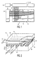
- Fig. 1 is a schematic block diagram of a conventional flat panel display system
- Fig. 2 is a perspective view of part of a conventional PALC display device
- Fig. 3 is a perspective view of a part of one form of a channel plate according to the invention for use in a PALC color display
- Fig. 4 is a top view of the spacer plate used in that channel plate
- Fig. 5 is an exploded side view of the channel plate of Fig. 3;
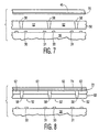
- Figs. 6 and 7 are exploded views illustrating two channel plate variants using etch stops in different ways in accordance with the invention.
- Fig. 8 is an exploded view of still further variants in accordance with the invention.
- Fig. 1 shows a flat panel display system 10, which represents a typical PALC display device and the operating electronic circuitry.
- the flat panel display system comprises a display panel 12 having a display surface 14 that contains a pattern formed by a rectangular planar array of nominally identical data storage or display elements 16 mutually spaced apart by predetermined distances in the vertical and horizontal directions.
- Each display element 16 in the array represents the overlapping portions of thin, narrow electrodes 18 arranged in vertical columns and elongate, narrow channels 20 arranged in horizontal rows.
- the electrodes 18 are hereinafter referred to from time to time as "column electrodes").
- the display elements 16 in each of the rows of channels 20 represent one line of data.
- column electrodes 18 and channels 20 determine the dimensions of display elements 16, which are typically of rectangular shape.
- Column electrodes 18 are deposited on a major surface of a first electrically nonconductive, optically transparent substrate 34 (Fig. 2), and the channel rows are usually built into a second transparent substrate 36.
- a first electrically nonconductive, optically transparent substrate 34 Fig. 2
- the channel rows are usually built into a second transparent substrate 36.
- Skilled persons will appreciate that certain systems, such as a reflective display of either the direct view or projection type, would require that only one substrate be optically transparent.
- Column electrodes 18 receive data drive signals of the analog voltage type developed on parallel output conductors 22' by different ones of output amplifiers 23 (Fig. 2) of a data driver or drive circuit 24, and channels 20 receive data strobe signals of the voltage pulse type developed on parallel output conductors 26' by different ones of output amplifiers 21 (Fig. 2) of a data strobe or strobe means or strobe circuit 28.
- Each of the channels 20 includes a reference electrode 30 (Fig. 2) to which a reference potential, such as ground, common to each channel 20 and data strobe 28 is applied.
- display system 10 employs a scan control circuit 32 that coordinates the functions of data driver 24 and data strobe 28 so that all columns of display elements 16 of display panel 12 are addressed row by row in row scan fashion as had been described.
- Display panel 12 may employ electro-optic materials of different types. For example, if it uses such material that changes the polarization state of incident light rays, display panel 12 is positioned between a pair of light polarizing filters, which cooperate with display panel 12 to change the luminance of light propagating through them. The use of a scattering liquid crystal cell as the electro-optic material would not require the use of polarizing filters, however.
- electro-optic materials All such materials or layers of materials which attenuate transmitted or reflected light in response to the voltage across it are referred to herein as electro-optic materials.
- LC materials are presently the most common example, the detailed description will refer to LC materials but it will be understood that the invention is not limited thereto.
- a color filter (not shown) may be positioned within display panel 12 to develop multi-colored images of controllable color intensity. For a projection display, color can also be achieved by using three separate monochrome panels 12, each of which controls one primary color.
- Fig. 2 illustrates the PALC version of such a flat display panel using LC material. Only 3 of the column electrodes 18 are shown.
- the row electrodes 20 are constituted by a plurality of parallel elongated sealed channels underlying (in Fig. 2) a layer 42 of the LC material. Each of the channels 20 is filled with an ionizable gas 44, closed off with a thin dielectric sheet 45 typically of glass, and contains on an interior channel surface first and second spaced elongated electrodes 30, 31 which extend the full length of each channel.
- the first electrode 30 is grounded and is commonly called the anode.
- the second electrode 31 is called the cathode, because to it will be supplied relative to the anode electrode a negative strobe pulse sufficient to cause electrons to be emitted from the cathode 31 to ionize the gas.
- each channel 20 has its gas ionized with a strobe pulse to form a plasma and a grounded line connection to a row of pixels in the LC layer 42 above.
- the strobe pulse terminates, and after deionization has occurred, the next channel is strobed and turned on. Since the column electrodes 18 each cross a whole column of pixels, typically only one plasma row connection at a time is allowed on to avoid crosstalk.
- Fabrication of a PALC device is typically done as described in the 1993 SID digest paper by providing first and second substrates 34, 36 with the first substrate 34 comprising a glass panel on which is vapor-deposited the ITO column electrodes 18, followed by color filter processing over the ITO electrodes to produce the RGB stripes (not shown), followed by the black surround processing and liquid crystal alignment processing.
- the second substrate 36 also a glass panel, is masked and etched to form the channels 20, following which the plasma electrode material is deposited and masked and etched to form the cathode 31 and anode 30 electrodes.
- a thin dielectric glass microsheet 45 is then sealed across the peripheral edges of the device to form with the ridges 50 the channels 20, which are then exhausted, back-filled with a low-pressure ionizable gas such as helium and/or neon and optionally with a small percentage of other noble gases and sealed off.
- a low-pressure ionizable gas such as helium and/or neon and optionally with a small percentage of other noble gases and sealed off.
- LC alignment of the exposed surface of the microsheet 45 is then carried out.
- the two assembled substrates are then assembled into a panel with the two LC alignment surfaces spaced apart and facing, the LC material 42 introduced into the space, and electrical connections made to the column electrodes 18 and plasma electrodes 30, 31.
- Fig. 3 is a perspective view of part of one form of channel plate 52 in accordance with the invention for one form of liquid crystal display panel in accordance with the invention.
- a thick flat glass bottom plate 36 forms a substantially transparent dielectric substrate for the plasma channels 20.
- Over the bottom plate 36 is deposited spaced electrode layer portions 30, 31.
- the channels walls are formed in a transparent dielectric sheet 50 substantially equal in thickness to the required channel depth.
- the dielectric sheet 50 is preferably of an etchable material, such as glass. This is accomplished with glass by etching through-holes 52 in the glass using conventional masking and etching processes.
- Two preferred ways for etching the glass to make the hole walls as close to the vertical as possible are as follows. In brief, this can be done as one-sided etching with an etch mask on one surface of the spacer plate and with relatively small openings in the etch mask and etching holes whose lateral dimensions are at least five times larger than the mask opening and the depth of the hole, in this case the thickness of the sheet 50. Using an isotropic etchant during the etching process, as the etching progresses, the sidewalls become steeper. The larger the lateral dimensions of the etched hole relative to the thickness of the glass sheet 50, the steeper the sidewalls.
- the mask hole is preferably 100 ⁇ m wide.
- the holes 52 would be elongated slots extending nearly the full length of the plate 50, but would terminate at opposite sides in an annular glass border region 53 so that the plate 50 remains as an integral element except for the holes 52 in the form of parallel slots spaced apart by spacer walls 58.
- the spacer walls can be made even more vertical by carrying out the etching from both sides of the plate 50.
- etch masks are required on both sides of the plate except where the holes are to be formed, and the mask holes overlie one another.
- the thickness of the channel sidewalls 58 thus produced represents the height of the channels 20 and constitute the spacers that space the thin dielectric sheet 45 that closes off the channels from the substrate 36, and thus the reference to the apertured plate 50 as the spacer plate.
- the etching can be by conventional chemical etchants or by conventional plasma etching. Alternatively, a mechanical erosion process can be substituted, such as sandblasting. This may be less costly and could also be used for materials for the spacer plate 50 that are more difficult to etch.
- the channel electrodes 30, 31 are separately deposited and patterned on the substrate 36 as described in the referenced papers and patents, after which the thin glass sheet 45 is attached over the apertured spacer plate 50, and the latter then aligned and attached to the substrate 36 containing the electrodes. As shown, by proper positioning of the electrodes and the spacer plate walls 58 so as to lie between adjacent electrode pairs 31, 30, then the glass spacer walls 58 would directly contact the glass substrate 36 surface. Adjacent channels 20 would each contain its own electrode pair. Because the glass walls are directly in contact with the glass substrate surface, or ion-containing layers on the surfaces, all three sheets 36, 50, 45 can be anodically bonded to each other thereby avoiding the frit sealing process. It will also be appreciated that the electrodes 30, 31 can be deposited on the substrate 36 after the spacer plate 50 has been bonded to the substrate 36 instead of before as described above.
- the walls 58 are shown with a slightly tapered shape, which would follow if the single-sided etching technique were used, as the glass surfaces closer to the mask hole would etch more than the more remote glass portions. If the double-sided etching process were used, then a double taper would result.
- anodic bonding preferably is used.
- Anodic bonding as such is a well known process for bonding two flat surfaces of ion-containing materials, such as glass.
- the glass sheets are placed against each other and an electric field applied across them while heating them to some intermediate elevated temperature which allows glass ions to become mobile.
- the ions migrate to the interface between the two sheets and pulls them together.
- the resultant force in the presence of heat, leads to the formation of a permanent bond between the two sheets. Typical temperatures are much lower than the softening temperature of the glass.
- the resultant assembled channel plate structure 52 is shown in Fig. 3.
- the remainder of the PALC panel can be fabricated in the usual way by filling and sealing the plasma panel and then forming the LC part of the panel on top of the thin glass sheet 45 as shown in Fig. 5 in an exploded view.
- the upper plate 34 may have deposited spacer members 60 which are aligned with the spacer walls 58 and act to space apart the upper structure 34 with its ITO electrodes 18 from the glass sheet 45 to provide a confined space for the LC material.
- Two variants of the invention use an etch stop layer to control penetration of the etchant into any etchable material attached to the spacer plate while the etching process is carried out.
- an etch stop layer 70 is deposited on the substrate 36.
- the etch stop layer 70 may be any thin ion-containing dielectric layer that will etch much slower, preferably at least five times slower, than the material of the spacer plate 50. Suitable materials are, for example, silicon nitride, or a thin amorphous silicon layer, to a thickness of, for example, 1 ⁇ m. Both of these materials etch much slower in an hydroborofluoric etchant for the glass spacer plate 50.
- the unetched spacer plate 50 can be attached as by anodic bonding to the deposited etch stop layer 70 which would be firmly bonded to the underlying substrate 36.
- deposited as used herein means a layer formed by a vapor-deposition process from a gas or vapor with or without an involved chemical reaction, or by a sputtering or evaporation process.
- the spacer plate 50 can be etched as described above in situ , while attached to the substrate 36. The etching is more easily carried out since the etch stop layer 70 will prevent etching of the glass substrate 36 while the etching of the slots 58 continues laterally to form the desired steep vertical walls.
- the spacer plate 50 is much thinner than the substrate 36 and thus more fragile, its handling and processing while bonded to the more rigid and stronger substrate 36 is facilitated.
- the electrodes 30, 31 can be deposited and patterned after the spacer slots 52 are formed.
- the thin dielectric sheet 45 can then be attached by frit sealing or preferably by anodic bonding to form the assembled channel plate.
- the etch stop layer 70 is deposited on the facing surface of the thin dielectric sheet 45.
- the unetched spacer plate 50 is then anodically bonded to the etch stop layer 70 as before, following which the spacer plate 50 is etched as also described before.
- the dielectric sheet 45 is much thinner and thus less rigid than the substrate 36.
- the border region 53 (Fig. 4) can be made wider or thicker to strengthen the spacer plate when attached to the thin dielectric sheet 45.
- the etch stop layer 70 can instead be deposited on the unetched spacer plate which is then bonded to the substrate 36 or the thin dielectric sheet 45 as the case may be so that the etch stop layer is positioned between the substrate or thin dielectric sheet and the spacer plate.
- crossbars 62 can be added to the spacer plate to strengthen the etched spacer plate.
- Fig. 8 illustrates still a further variant which enables omitting of the thin dielectric sheet 45 as a separate element.
- a continuous etch stop dielectric layer 72 is deposited as shown on the outer surface of the unetched spacer plate 50.
- This etch stop layer can be made much thicker, for example, 50 ⁇ m thick, i.e., thick enough to be sufficiently self-supporting to span the subsequently etched slots 52 without breaking or being otherwise damaged.
- a thin etch stop layer 72 can be used as before but with additional continuous layers 74 deposited on top to increase its strength.
- the etch stop 72 can be, for example, of silicon nitride or amorphous silicon, with a thicker deposited dielectric top layer 74, for example, of spin-on glass or low-temperature deposited silicon dioxide.
- the slots 52 are then etched in the spacer plate 50, the etch stop layer 72 serving to prevent etching of the materials of the single or multi-layer deposit 74 above.
- the completed etched spacer plate 50, with the continuous layers 72, 74 serving now as the thin dielectric sheet to seal off the tops of the channels 20, can be attached to the substrate 36. In this case, anodic bonding or glass frit bonding can be used. In this modification, a separate top sheet 45 is unnecessary.
- the etching of the slots 58 may be desirable to limit the etching of the slots 58 to the active region to be used as the display area of the completed device, so that the frit sealing for sealing the electrodes where they exit the discharge space does not come into contact with the thin deposited layers 72, 74 which seal off the top of the channels 20.
- the electrode materials are typically of a metal such as copper, or layers of Cu-Cr-Cu, or other suitable metals.
- the width of the channels 20 may be large, or where the thin spacer plate 50 acts as the substrate for the deposited layers 72, 74, it may be desirable to increase the mechanical strength of the spacer plate 50.
- This can be done as illustrated in Fig. 8 by etching strengthening crossbars 62 in the spacer plate 50.
- the crossbars 62 which extend laterally to and between the spacer walls 58 are thus integral with the plate 60.
- their height can be reduced without reducing the height of the spacer walls 58.
- the crosssbars can be made so that they do not extend all the way to the height of the channels 20.
- the invention is generally applicable to all kinds of flat displays, and in particular to displays of the plasma-addressed type, especially PALC displays that typically have a small channel pitch for use in computer monitors, workstations or TV applications. While the main application of the channel plate of the invention is in PALC type display devices, the same plasma plate construction 52 can also be used as a plasma display device where the output is the light, generated by the plasma, which can exit the device via the transparent substrate and/or the overlying transparent sheet-like member.
- Fig. 3 embodiment Several preferred examples for the Fig. 3 embodiment are (all values are in ⁇ m): a wall width of about 20-50; a wall height of about 50-160; and a wall pitch of about 200-500.
- channels in the substrate are typically straight, the invention is not limited to such a configuration and other channel shapes, such as a meandering shape, are also possible within the scope of the invention.
Landscapes
- Physics & Mathematics (AREA)
- Nonlinear Science (AREA)
- Chemical & Material Sciences (AREA)
- Crystallography & Structural Chemistry (AREA)
- General Physics & Mathematics (AREA)
- Engineering & Computer Science (AREA)
- Plasma & Fusion (AREA)
- Mathematical Physics (AREA)
- Optics & Photonics (AREA)
- Theoretical Computer Science (AREA)
- Liquid Crystal (AREA)
- Gas-Filled Discharge Tubes (AREA)
- Devices For Indicating Variable Information By Combining Individual Elements (AREA)
Claims (15)
- Kanalplatte (52) für eine flache Wiedergabeanordnung mit länglichen Kanälen (20) auf dem dielektrischen Substrat (36) mit einer im Wesentlichen planaren oberen Fläche, mit Mitteln (50), die kanaldefinierende flankierende Wandteile (58) auf der oberen Fläche des Substrats bilden, mit Elektrodenflächen (30,31) in jedem der Kanäle und mit einem dünnen plattenartigen Element (45) über die flankierenden Wandteile, dadurch gekennzeichnet, dass das Mittel, das die kanaldefinierenden flankierenden Wandteile bilden in Form einer Distanzplatte (50) ist, die eine integrale dielektrische Platte aufweist, die unmittelbar die obere Fläche des Substrats (36) kontaktiert, wobei diese Platte (50), was die Dicke anbelangt, im Wesentlichen der erforderlichen Kanaltiefe entspricht und längliche durchgehende Löcher (52) aufweist welche die flankierenden Wandteile (58) definieren, wobei die flankierenden Wandteile mit der oberen Fläche des Substrats in direktem Kontakt stehen, wodurch die obere Fläche des Substrats, die flankierenden Wandteile und das dünne dielektrische plattenartige Element zusammen die länglichen Kanäle definieren.
- Kanalplatte nach Anspruch 1, dadurch gekennzeichnet, dass das dünne dielektrische plattenartige Element (45), die dielektrische Platte (50) und das Substrat (36) aus Glas bestehen.
- Kanalplatte nach Anspruch 1, dadurch gekennzeichnet, dass die flankierenden Wandteile (58) an ihrem Umfang durch einen integralen Randbereich (53) der Distanzplatte zusammengefügt worden sind.
- Kanalplatte nach Anspruch 1, dadurch gekennzeichnet, dass die durchgehenden Löcher (52) lateral in einem Abstand voneinander liegende geätzte Schlitze sind (52).
- Kanalplatte nach Anspruch 1, dadurch gekennzeichnet, dass das Substrat (36) und die flankierenden Wandteile (58) der Distanzplatte anodisch verbunden worden sind.
- Kanalplatte nach Anspruch 1, dadurch gekennzeichnet, dass die obere Fläche des Substrats (36) eine Ätzsperrschicht (70) aufweist.
- Kanalplatte nach Anspruch 1, dadurch gekennzeichnet, dass das dünne dielektrische plattenartige Element (45) unmittelbar an den flankierenden Wandteilen (58) der Distanzplatte befestigt sind.
- Kanalplatte nach Anspruch 4, dadurch gekennzeichnet, dass das dünne dielektrische plattenartige Element (45) eine kontinuierliche abgelagerte Schicht (72, 74) auf der Oberfläche der Distanzplatte aufweist, und zwar in einem Abstand von dem Substrat und sich über die geätzten Schlitze (52) erstreckend, und dass die kontinuierliche abgelagerte Schicht eine Ätzsperrschicht aufweist.
- Kanalplatte nach einem der vorstehenden Ansprüche, dadurch gekennzeichnet, dass die Kanäle mit einer plasmabildenden Atmosphäre (44) gefüllt sind.
- Verfahren zum Herstellen einer Kanalplatte für eine flache Wiedergabeanordnung mit länglichen Kanälen (20) auf einem dielektrischen Substrat (36), die je durch in einem Abstand voneinander liegende flankierende Wandteile (58) auf dem Substrat definiert werden und ein Paar Elektroden (30, 31) aufweisen, wobei dieses Verfahren die nachfolgenden Verfahrensschritte umfasst:(a) das Schaffen eines im Wesentlichen transparenten dielektrischen Substrats (36) mit einer im Wesentlichen planaren oberen Fläche,(b) das Schaffen einer im Wesentlichen transparenten Distanzplatte (50) mit einer integralen dielektrischen Platte mit einer ersten und einer gegenüber liegenden zweiten Fläche,(c) das in der Distanzplatte Bilden einer Anzahl im Wesentlichen in gleichen Abständen voneinander liegender, flankierender Wandteile (58), die je eine Höhe haben, die der Dicke der Distanzplatte zwischen der ersten und der zweiten Fläche entspricht,(d) das Anbringen eines dünnen dielektrischen plattenarigen Elementes (45) über die erste Fläche der Distanzplatte,(e) das Ablagern eines elektrisch leitenden Materials über die obere Fläche des Substrats um auf dem Substrat Paare von in einem Abstand voneinander liegenden Elektroden (30, 31) zu bilden,(f) das Anbringen der Distanzplatte (50) mittels der zweiten Fläche unmittelbar an der oberen Fläche des Substrats (36), wobei die in einem Abstand voneinander liegenden flankierenden Wandteile sich im Allgemeinen quer zu dem Substrat erstrecken zum Definieren länglicher Kanäle (20) und derart, dass in einem Abstand voneinander liegende Elektroden zwischen jedem benachbarten Paar flankierender Wandteile liegen.
- Verfahren zum Herstellen einer Kanalplatte für eine flache Wiedergabeanordnung mit länglichen Kanälen (20) auf dem dielektrischen Substrat (36), die je durch in einem Abstand voneinander liegende flankierende Wandteile (58) auf dem Substrat definiert sind und ein Paar Elektroden (30, 31) aufweisen, wobei dieses Verfahren die nachfolgenden Verfahrensschritte umfasst:(a) das Schaffen eines im Wesentlichen transparenten dielektrischen Substrats (36) mit einer im Wesentlichen planaren oberen Fläche,(b) das Schaffen einer im Wesentlichen transparenten Distanzplatte (50) mit einer integralen dielektrischen Platte mit einer ersten und einer derselben gegenüberliegenden zweiten Fläche,(c) das Schaffen eines dünnen dielektrischen plattenartigen Elementes (45),(d) das Bilden einer Ätzsperrschicht auf einer Fläche des Substrats oder auf einer Fläche der Distanzplatte, oder auf einer Fläche des dünnen dielektrischen plattenartigen Elementes,(e) das Anbringen der Distanzplatte mittels der ersten Fläche auf der oberen Fläche des Substrats (36) oder auf dem dünnen dielektrischen plattenförmigen Element (45), so dass die Ätzsperrschicht zwischen der Distanzplatte und dem dünnen dielektrischen plattenartigen Element oder zwischen der Distanzplatte und dem Substrat liegt,(f) das darauffolgende Bilden einer Anzahl im Wesentlichen in gleichen Abständen voneinander liegender flankierender Wandteile (58) in der Distanzplatte, wobei diese Wandteile je eine Höhe haben, die der Dicke der Distanzplatte entspricht, und zwar dadurch, dass Schlitze (52) in der Distanzplatte eingeätzt werden, dies alles unter Verwendung eines Ätzmittels, das die Ätzsperrschicht nur leicht angreift,(g) das Ablagern eines elektrisch leitenden Materials über die obere Fläche des Substrats um auf dem Substrat Paare in einem Abstand voneinander liegender Elektroden (30, 31) für jeden Kanal zu bilden, und(h) entweder das Anbringen des dünnen dielektrischen plattenartigen Elementes (45) über die zweite Fläche der Distanzplatte (50) in einem Abstand von dem Substrat oder das Anbringen der Distanzplatte mittels der zweiten Fläche an der oberen Fläche des Substrats.
- Verfahren nach Anspruch 10 oder 11, wobei das Substrat (36), die Distanzplatte (50) und das dünne dielektrische plattenartige Element (45) aus Glas gebildet sind.
- Verfahren nach Anspruch 10, wobei der Verfahrensschritt (f) durch anodisches Verbinden der Distanzplatte mit dem Substrat durchgeführt wird.
- Verfahren nach Anspruch 10, wobei der Verfahrensschritt (d) durch anodisches Verbinden der Distanzplatte mit dem dünnen dielektrischen plattenartigen Element durchgeführt wird.
- Verfahren nach einem der Ansprüche 10 bis 14, wobei das Verfahren den weiteren Verfahrensschritt umfasst, wobei die Kanäle mit einer plasmabildenden Atmosphäre (44) gefüllt wird.
Applications Claiming Priority (3)
| Application Number | Priority Date | Filing Date | Title |
|---|---|---|---|
| US588799 | 1996-01-19 | ||
| US08/588,799 US5804920A (en) | 1996-01-19 | 1996-01-19 | Plasma addressed liquid crystal display with etched glass spacers |
| PCT/IB1996/001424 WO1997026641A1 (en) | 1996-01-19 | 1996-12-12 | Plasma addressed liquid crystal display with etched glass spacers |
Publications (2)
| Publication Number | Publication Date |
|---|---|
| EP0815549A1 EP0815549A1 (de) | 1998-01-07 |
| EP0815549B1 true EP0815549B1 (de) | 2001-10-24 |
Family
ID=24355343
Family Applications (1)
| Application Number | Title | Priority Date | Filing Date |
|---|---|---|---|
| EP96940074A Expired - Lifetime EP0815549B1 (de) | 1996-01-19 | 1996-12-12 | Kanalplatte für eine flache anzeigevorrichtung und verfahren zur herstellung einer solchen platte |
Country Status (6)
| Country | Link |
|---|---|
| US (3) | US5804920A (de) |
| EP (1) | EP0815549B1 (de) |
| KR (1) | KR19980703117A (de) |
| CN (1) | CN1120461C (de) |
| DE (1) | DE69616297T2 (de) |
| WO (1) | WO1997026641A1 (de) |
Families Citing this family (16)
| Publication number | Priority date | Publication date | Assignee | Title |
|---|---|---|---|---|
| US5804920A (en) * | 1996-01-19 | 1998-09-08 | Philips Electronics North America Corporation | Plasma addressed liquid crystal display with etched glass spacers |
| US6118213A (en) * | 1996-06-28 | 2000-09-12 | Tektronix, Inc. | Plasma addressed liquid crystal display device with integrated source of reactive gas |
| TW385470B (en) * | 1997-10-24 | 2000-03-21 | Tektronix Inc | Cathode structure for a PALC panel |
| JP3559719B2 (ja) * | 1998-01-13 | 2004-09-02 | キヤノン株式会社 | プラズマアドレス型の液晶表示装置 |
| DE19841900A1 (de) * | 1998-09-11 | 2000-03-30 | Schott Glas | Verfahren zum Aufbringen von metallischen Leiterbahnen als Elektroden auf eine Kanalplatte für großflächige Flachbildschirme |
| WO2000048218A1 (en) * | 1999-02-12 | 2000-08-17 | Toppan Printing Co., Ltd. | Plasma display panel, method and device for production therefor |
| US6597412B1 (en) * | 1999-04-28 | 2003-07-22 | Tektronix, Inc. | Liquid crystal display device employing fiber spacers |
| US6783948B1 (en) * | 1999-07-30 | 2004-08-31 | Bayer Corporation | Chemiluminescent acridinium compounds and analogues thereof as substrates of hydrolytic enzymes |
| JP2002025453A (ja) * | 2000-06-15 | 2002-01-25 | Koninkl Philips Electronics Nv | ドーパントガス分圧制御機能を有するプラズマアドレス表示装置 |
| US6944032B1 (en) * | 2001-04-12 | 2005-09-13 | Rockwell Collins | Interconnect for flat panel displays |
| JP2002334670A (ja) * | 2001-05-09 | 2002-11-22 | Hitachi Ltd | 表示装置 |
| KR100814806B1 (ko) * | 2001-10-15 | 2008-03-19 | 삼성에스디아이 주식회사 | 스페이서 제조 방법 및 이 스페이서를 갖는 평판 표시 소자 |
| US20050135759A1 (en) * | 2003-12-22 | 2005-06-23 | Xingwu Wang | Optical fiber assembly |
| JP2003249182A (ja) * | 2002-02-22 | 2003-09-05 | Hitachi Ltd | 表示装置 |
| CN102262464B (zh) * | 2010-05-25 | 2014-10-29 | 深圳富泰宏精密工业有限公司 | 触控式透明键盘 |
| JP2015215502A (ja) * | 2014-05-12 | 2015-12-03 | 日本電気硝子株式会社 | ガラスセル、液晶素子及びこれらの製造方法 |
Family Cites Families (19)
| Publication number | Priority date | Publication date | Assignee | Title |
|---|---|---|---|---|
| US5272472A (en) * | 1988-01-19 | 1993-12-21 | Tektronix, Inc. | Apparatus for addressing data storage elements with an ionizable gas excited by an AC energy source |
| US5077553A (en) * | 1988-01-19 | 1991-12-31 | Tektronix, Inc. | Apparatus for and methods of addressing data storage elements |
| US4896149A (en) * | 1988-01-19 | 1990-01-23 | Tektronix, Inc. | Addressing structure using ionizable gaseous medium |
| JP3013470B2 (ja) * | 1991-02-20 | 2000-02-28 | ソニー株式会社 | 画像表示装置 |
| KR940006301B1 (ko) * | 1991-10-29 | 1994-07-14 | 삼성전관 주식회사 | 프라즈마 어드레스 방식의 액정표시소자와 그 제조방법 |
| US5205770A (en) * | 1992-03-12 | 1993-04-27 | Micron Technology, Inc. | Method to form high aspect ratio supports (spacers) for field emission display using micro-saw technology |
| US5424605A (en) * | 1992-04-10 | 1995-06-13 | Silicon Video Corporation | Self supporting flat video display |
| US5276384A (en) * | 1992-08-26 | 1994-01-04 | Tektronix, Inc. | Electrode configuration for channel confinement of plasma discharge in an electrode structure using an ionizable gaseous medium |
| US5440201A (en) * | 1992-08-26 | 1995-08-08 | Tektronix, Inc. | Plasma addressing structure with wide or transparent reference electrode |
| TW228592B (de) * | 1992-08-26 | 1994-08-21 | Tektronix Inc | |
| US5537234A (en) * | 1993-01-19 | 1996-07-16 | Hughes Aircraft Company | Relective liquid crystal display including driver devices integrally formed in monocrystalline semiconductor layer and method of fabricating the display |
| WO1994020975A1 (en) * | 1993-03-11 | 1994-09-15 | Fed Corporation | Emitter tip structure and field emission device comprising same, and method of making same |
| US5395481A (en) * | 1993-10-18 | 1995-03-07 | Regents Of The University Of California | Method for forming silicon on a glass substrate |
| JPH08313884A (ja) * | 1995-05-12 | 1996-11-29 | Sony Corp | 放電パネル |
| US5804920A (en) * | 1996-01-19 | 1998-09-08 | Philips Electronics North America Corporation | Plasma addressed liquid crystal display with etched glass spacers |
| US5777432A (en) * | 1997-04-07 | 1998-07-07 | Motorola Inc. | High breakdown field emission device with tapered cylindrical spacers |
| US6249083B1 (en) * | 1998-01-12 | 2001-06-19 | Samsung Display Devices Co., Ltd. | Electric field emission display (FED) and method of manufacturing spacer thereof |
| JP2000156277A (ja) * | 1998-04-24 | 2000-06-06 | Canon Inc | 加熱装置及び加熱方法 |
| US6004179A (en) * | 1998-10-26 | 1999-12-21 | Micron Technology, Inc. | Methods of fabricating flat panel evacuated displays |
-
1996
- 1996-01-19 US US08/588,799 patent/US5804920A/en not_active Expired - Fee Related
- 1996-12-12 CN CN96193795A patent/CN1120461C/zh not_active Expired - Fee Related
- 1996-12-12 DE DE69616297T patent/DE69616297T2/de not_active Expired - Fee Related
- 1996-12-12 KR KR1019970706519A patent/KR19980703117A/ko not_active Ceased
- 1996-12-12 EP EP96940074A patent/EP0815549B1/de not_active Expired - Lifetime
- 1996-12-12 WO PCT/IB1996/001424 patent/WO1997026641A1/en not_active Ceased
-
1998
- 1998-06-11 US US09/096,073 patent/US6285127B1/en not_active Expired - Fee Related
-
2001
- 2001-07-23 US US09/911,054 patent/US6517402B1/en not_active Expired - Fee Related
Also Published As
| Publication number | Publication date |
|---|---|
| DE69616297D1 (de) | 2001-11-29 |
| WO1997026641A1 (en) | 1997-07-24 |
| CN1183845A (zh) | 1998-06-03 |
| US6285127B1 (en) | 2001-09-04 |
| US6517402B1 (en) | 2003-02-11 |
| CN1120461C (zh) | 2003-09-03 |
| EP0815549A1 (de) | 1998-01-07 |
| KR19980703117A (ko) | 1998-10-15 |
| US5804920A (en) | 1998-09-08 |
| DE69616297T2 (de) | 2002-07-25 |
Similar Documents
| Publication | Publication Date | Title |
|---|---|---|
| EP0815549B1 (de) | Kanalplatte für eine flache anzeigevorrichtung und verfahren zur herstellung einer solchen platte | |
| EP0811219B1 (de) | Kanalplatte mit aus organischem material bestehenden wänden für eine plasmagesteuerte anzeigevorrichtung sowie verfahren zur herstellung einer solchen platte | |
| EP0811220B1 (de) | Aus elementen zusammengesetzte kanalplatte für eine plasmaadressierte flache anzeigevorrichtung und verfahren zur herstellung einer solchen platte | |
| US6579462B2 (en) | Plasma addressed liquid crystal display with glass spacers | |
| US5914562A (en) | Anodic bonded plasma addressed liquid crystal displays | |
| EP0763228B1 (de) | Plasma-adressierbare flüssigkristallanzeigevorrichtung mit geätzten elektroden | |
| US6007399A (en) | Hollow cathodes for plasma-containing display devices and method of producing same | |
| EP0760992B1 (de) | Plasmagesteuerte flüssigkristallanzeige mit geätztem plasmakanälen | |
| EP0746836B1 (de) | Kanalanordnung für plasmagesteuerte flüssigkristallanzeigevorrichtung | |
| US6057895A (en) | Plasmas addressed liquid crystal display with deposited plasma channels with tapered edges | |
| JP2000501205A (ja) | 食刻ガラススペーサを具えるプラズマアドレス液晶ディスプレイ装置 |
Legal Events
| Date | Code | Title | Description |
|---|---|---|---|
| PUAI | Public reference made under article 153(3) epc to a published international application that has entered the european phase |
Free format text: ORIGINAL CODE: 0009012 |
|
| AK | Designated contracting states |
Kind code of ref document: A1 Designated state(s): DE FR GB NL |
|
| 17P | Request for examination filed |
Effective date: 19980126 |
|
| RAP3 | Party data changed (applicant data changed or rights of an application transferred) |
Owner name: KONINKLIJKE PHILIPS ELECTRONICS N.V. |
|
| 17Q | First examination report despatched |
Effective date: 19990909 |
|
| GRAG | Despatch of communication of intention to grant |
Free format text: ORIGINAL CODE: EPIDOS AGRA |
|
| RTI1 | Title (correction) |
Free format text: CHANNEL PLATE FOR A FLAT DISPLAY AND METHOD OF MANUFACTURING THEREOF |
|
| GRAG | Despatch of communication of intention to grant |
Free format text: ORIGINAL CODE: EPIDOS AGRA |
|
| GRAH | Despatch of communication of intention to grant a patent |
Free format text: ORIGINAL CODE: EPIDOS IGRA |
|
| GRAH | Despatch of communication of intention to grant a patent |
Free format text: ORIGINAL CODE: EPIDOS IGRA |
|
| GRAA | (expected) grant |
Free format text: ORIGINAL CODE: 0009210 |
|
| AK | Designated contracting states |
Kind code of ref document: B1 Designated state(s): DE FR GB NL |
|
| PG25 | Lapsed in a contracting state [announced via postgrant information from national office to epo] |
Ref country code: NL Free format text: LAPSE BECAUSE OF FAILURE TO SUBMIT A TRANSLATION OF THE DESCRIPTION OR TO PAY THE FEE WITHIN THE PRESCRIBED TIME-LIMIT Effective date: 20011024 |
|
| REF | Corresponds to: |
Ref document number: 69616297 Country of ref document: DE Date of ref document: 20011129 |
|
| REG | Reference to a national code |
Ref country code: GB Ref legal event code: IF02 |
|
| ET | Fr: translation filed | ||
| NLV1 | Nl: lapsed or annulled due to failure to fulfill the requirements of art. 29p and 29m of the patents act | ||
| PLBE | No opposition filed within time limit |
Free format text: ORIGINAL CODE: 0009261 |
|
| STAA | Information on the status of an ep patent application or granted ep patent |
Free format text: STATUS: NO OPPOSITION FILED WITHIN TIME LIMIT |
|
| REG | Reference to a national code |
Ref country code: GB Ref legal event code: 746 Effective date: 20020918 |
|
| 26N | No opposition filed | ||
| REG | Reference to a national code |
Ref country code: FR Ref legal event code: D6 |
|
| PGFP | Annual fee paid to national office [announced via postgrant information from national office to epo] |
Ref country code: FR Payment date: 20021223 Year of fee payment: 7 |
|
| PGFP | Annual fee paid to national office [announced via postgrant information from national office to epo] |
Ref country code: GB Payment date: 20021224 Year of fee payment: 7 |
|
| PGFP | Annual fee paid to national office [announced via postgrant information from national office to epo] |
Ref country code: DE Payment date: 20030217 Year of fee payment: 7 |
|
| PG25 | Lapsed in a contracting state [announced via postgrant information from national office to epo] |
Ref country code: GB Free format text: LAPSE BECAUSE OF NON-PAYMENT OF DUE FEES Effective date: 20031212 |
|
| PG25 | Lapsed in a contracting state [announced via postgrant information from national office to epo] |
Ref country code: DE Free format text: LAPSE BECAUSE OF NON-PAYMENT OF DUE FEES Effective date: 20040701 |
|
| GBPC | Gb: european patent ceased through non-payment of renewal fee |
Effective date: 20031212 |
|
| PG25 | Lapsed in a contracting state [announced via postgrant information from national office to epo] |
Ref country code: FR Free format text: LAPSE BECAUSE OF NON-PAYMENT OF DUE FEES Effective date: 20040831 |
|
| REG | Reference to a national code |
Ref country code: FR Ref legal event code: ST |