EP0816896A2 - Composant électrooptique - Google Patents
Composant électrooptique Download PDFInfo
- Publication number
- EP0816896A2 EP0816896A2 EP97401380A EP97401380A EP0816896A2 EP 0816896 A2 EP0816896 A2 EP 0816896A2 EP 97401380 A EP97401380 A EP 97401380A EP 97401380 A EP97401380 A EP 97401380A EP 0816896 A2 EP0816896 A2 EP 0816896A2
- Authority
- EP
- European Patent Office
- Prior art keywords
- modulators
- optical
- component according
- converter
- guide
- Prior art date
- Legal status (The legal status is an assumption and is not a legal conclusion. Google has not performed a legal analysis and makes no representation as to the accuracy of the status listed.)
- Granted
Links
Images


Classifications
-
- G—PHYSICS
- G02—OPTICS
- G02B—OPTICAL ELEMENTS, SYSTEMS OR APPARATUS
- G02B6/00—Light guides; Structural details of arrangements comprising light guides and other optical elements, e.g. couplings
- G02B6/10—Light guides; Structural details of arrangements comprising light guides and other optical elements, e.g. couplings of the optical waveguide type
- G02B6/12—Light guides; Structural details of arrangements comprising light guides and other optical elements, e.g. couplings of the optical waveguide type of the integrated circuit kind
- G02B6/122—Basic optical elements, e.g. light-guiding paths
- G02B6/125—Bends, branchings or intersections
-
- G—PHYSICS
- G02—OPTICS
- G02F—OPTICAL DEVICES OR ARRANGEMENTS FOR THE CONTROL OF LIGHT BY MODIFICATION OF THE OPTICAL PROPERTIES OF THE MEDIA OF THE ELEMENTS INVOLVED THEREIN; NON-LINEAR OPTICS; FREQUENCY-CHANGING OF LIGHT; OPTICAL LOGIC ELEMENTS; OPTICAL ANALOGUE/DIGITAL CONVERTERS
- G02F1/00—Devices or arrangements for the control of the intensity, colour, phase, polarisation or direction of light arriving from an independent light source, e.g. switching, gating or modulating; Non-linear optics
- G02F1/01—Devices or arrangements for the control of the intensity, colour, phase, polarisation or direction of light arriving from an independent light source, e.g. switching, gating or modulating; Non-linear optics for the control of the intensity, phase, polarisation or colour
- G02F1/03—Devices or arrangements for the control of the intensity, colour, phase, polarisation or direction of light arriving from an independent light source, e.g. switching, gating or modulating; Non-linear optics for the control of the intensity, phase, polarisation or colour based on ceramics or electro-optical crystals, e.g. exhibiting Pockels effect or Kerr effect
- G02F1/035—Devices or arrangements for the control of the intensity, colour, phase, polarisation or direction of light arriving from an independent light source, e.g. switching, gating or modulating; Non-linear optics for the control of the intensity, phase, polarisation or colour based on ceramics or electro-optical crystals, e.g. exhibiting Pockels effect or Kerr effect in an optical waveguide structure
- G02F1/0353—Devices or arrangements for the control of the intensity, colour, phase, polarisation or direction of light arriving from an independent light source, e.g. switching, gating or modulating; Non-linear optics for the control of the intensity, phase, polarisation or colour based on ceramics or electro-optical crystals, e.g. exhibiting Pockels effect or Kerr effect in an optical waveguide structure involving an electro-optic TE-TM mode conversion
-
- G—PHYSICS
- G02—OPTICS
- G02F—OPTICAL DEVICES OR ARRANGEMENTS FOR THE CONTROL OF LIGHT BY MODIFICATION OF THE OPTICAL PROPERTIES OF THE MEDIA OF THE ELEMENTS INVOLVED THEREIN; NON-LINEAR OPTICS; FREQUENCY-CHANGING OF LIGHT; OPTICAL LOGIC ELEMENTS; OPTICAL ANALOGUE/DIGITAL CONVERTERS
- G02F1/00—Devices or arrangements for the control of the intensity, colour, phase, polarisation or direction of light arriving from an independent light source, e.g. switching, gating or modulating; Non-linear optics
- G02F1/01—Devices or arrangements for the control of the intensity, colour, phase, polarisation or direction of light arriving from an independent light source, e.g. switching, gating or modulating; Non-linear optics for the control of the intensity, phase, polarisation or colour
- G02F1/061—Devices or arrangements for the control of the intensity, colour, phase, polarisation or direction of light arriving from an independent light source, e.g. switching, gating or modulating; Non-linear optics for the control of the intensity, phase, polarisation or colour based on electro-optical organic material
- G02F1/065—Devices or arrangements for the control of the intensity, colour, phase, polarisation or direction of light arriving from an independent light source, e.g. switching, gating or modulating; Non-linear optics for the control of the intensity, phase, polarisation or colour based on electro-optical organic material in an optical waveguide structure
-
- G—PHYSICS
- G02—OPTICS
- G02F—OPTICAL DEVICES OR ARRANGEMENTS FOR THE CONTROL OF LIGHT BY MODIFICATION OF THE OPTICAL PROPERTIES OF THE MEDIA OF THE ELEMENTS INVOLVED THEREIN; NON-LINEAR OPTICS; FREQUENCY-CHANGING OF LIGHT; OPTICAL LOGIC ELEMENTS; OPTICAL ANALOGUE/DIGITAL CONVERTERS
- G02F1/00—Devices or arrangements for the control of the intensity, colour, phase, polarisation or direction of light arriving from an independent light source, e.g. switching, gating or modulating; Non-linear optics
- G02F1/01—Devices or arrangements for the control of the intensity, colour, phase, polarisation or direction of light arriving from an independent light source, e.g. switching, gating or modulating; Non-linear optics for the control of the intensity, phase, polarisation or colour
- G02F1/03—Devices or arrangements for the control of the intensity, colour, phase, polarisation or direction of light arriving from an independent light source, e.g. switching, gating or modulating; Non-linear optics for the control of the intensity, phase, polarisation or colour based on ceramics or electro-optical crystals, e.g. exhibiting Pockels effect or Kerr effect
- G02F1/035—Devices or arrangements for the control of the intensity, colour, phase, polarisation or direction of light arriving from an independent light source, e.g. switching, gating or modulating; Non-linear optics for the control of the intensity, phase, polarisation or colour based on ceramics or electro-optical crystals, e.g. exhibiting Pockels effect or Kerr effect in an optical waveguide structure
- G02F1/0356—Devices or arrangements for the control of the intensity, colour, phase, polarisation or direction of light arriving from an independent light source, e.g. switching, gating or modulating; Non-linear optics for the control of the intensity, phase, polarisation or colour based on ceramics or electro-optical crystals, e.g. exhibiting Pockels effect or Kerr effect in an optical waveguide structure controlled by a high-frequency electromagnetic wave component in an electric waveguide structure
-
- G—PHYSICS
- G02—OPTICS
- G02F—OPTICAL DEVICES OR ARRANGEMENTS FOR THE CONTROL OF LIGHT BY MODIFICATION OF THE OPTICAL PROPERTIES OF THE MEDIA OF THE ELEMENTS INVOLVED THEREIN; NON-LINEAR OPTICS; FREQUENCY-CHANGING OF LIGHT; OPTICAL LOGIC ELEMENTS; OPTICAL ANALOGUE/DIGITAL CONVERTERS
- G02F1/00—Devices or arrangements for the control of the intensity, colour, phase, polarisation or direction of light arriving from an independent light source, e.g. switching, gating or modulating; Non-linear optics
- G02F1/01—Devices or arrangements for the control of the intensity, colour, phase, polarisation or direction of light arriving from an independent light source, e.g. switching, gating or modulating; Non-linear optics for the control of the intensity, phase, polarisation or colour
- G02F1/21—Devices or arrangements for the control of the intensity, colour, phase, polarisation or direction of light arriving from an independent light source, e.g. switching, gating or modulating; Non-linear optics for the control of the intensity, phase, polarisation or colour by interference
- G02F1/212—Mach-Zehnder type
-
- G—PHYSICS
- G02—OPTICS
- G02F—OPTICAL DEVICES OR ARRANGEMENTS FOR THE CONTROL OF LIGHT BY MODIFICATION OF THE OPTICAL PROPERTIES OF THE MEDIA OF THE ELEMENTS INVOLVED THEREIN; NON-LINEAR OPTICS; FREQUENCY-CHANGING OF LIGHT; OPTICAL LOGIC ELEMENTS; OPTICAL ANALOGUE/DIGITAL CONVERTERS
- G02F1/00—Devices or arrangements for the control of the intensity, colour, phase, polarisation or direction of light arriving from an independent light source, e.g. switching, gating or modulating; Non-linear optics
- G02F1/01—Devices or arrangements for the control of the intensity, colour, phase, polarisation or direction of light arriving from an independent light source, e.g. switching, gating or modulating; Non-linear optics for the control of the intensity, phase, polarisation or colour
- G02F1/21—Devices or arrangements for the control of the intensity, colour, phase, polarisation or direction of light arriving from an independent light source, e.g. switching, gating or modulating; Non-linear optics for the control of the intensity, phase, polarisation or colour by interference
- G02F1/225—Devices or arrangements for the control of the intensity, colour, phase, polarisation or direction of light arriving from an independent light source, e.g. switching, gating or modulating; Non-linear optics for the control of the intensity, phase, polarisation or colour by interference in an optical waveguide structure
-
- G—PHYSICS
- G02—OPTICS
- G02F—OPTICAL DEVICES OR ARRANGEMENTS FOR THE CONTROL OF LIGHT BY MODIFICATION OF THE OPTICAL PROPERTIES OF THE MEDIA OF THE ELEMENTS INVOLVED THEREIN; NON-LINEAR OPTICS; FREQUENCY-CHANGING OF LIGHT; OPTICAL LOGIC ELEMENTS; OPTICAL ANALOGUE/DIGITAL CONVERTERS
- G02F1/00—Devices or arrangements for the control of the intensity, colour, phase, polarisation or direction of light arriving from an independent light source, e.g. switching, gating or modulating; Non-linear optics
- G02F1/29—Devices or arrangements for the control of the intensity, colour, phase, polarisation or direction of light arriving from an independent light source, e.g. switching, gating or modulating; Non-linear optics for the control of the position or the direction of light beams, i.e. deflection
- G02F1/31—Digital deflection, i.e. optical switching
- G02F1/313—Digital deflection, i.e. optical switching in an optical waveguide structure
- G02F1/3132—Digital deflection, i.e. optical switching in an optical waveguide structure of directional coupler type
-
- G—PHYSICS
- G02—OPTICS
- G02F—OPTICAL DEVICES OR ARRANGEMENTS FOR THE CONTROL OF LIGHT BY MODIFICATION OF THE OPTICAL PROPERTIES OF THE MEDIA OF THE ELEMENTS INVOLVED THEREIN; NON-LINEAR OPTICS; FREQUENCY-CHANGING OF LIGHT; OPTICAL LOGIC ELEMENTS; OPTICAL ANALOGUE/DIGITAL CONVERTERS
- G02F1/00—Devices or arrangements for the control of the intensity, colour, phase, polarisation or direction of light arriving from an independent light source, e.g. switching, gating or modulating; Non-linear optics
- G02F1/29—Devices or arrangements for the control of the intensity, colour, phase, polarisation or direction of light arriving from an independent light source, e.g. switching, gating or modulating; Non-linear optics for the control of the position or the direction of light beams, i.e. deflection
- G02F1/31—Digital deflection, i.e. optical switching
- G02F1/313—Digital deflection, i.e. optical switching in an optical waveguide structure
- G02F1/3136—Digital deflection, i.e. optical switching in an optical waveguide structure of interferometric switch type
-
- G—PHYSICS
- G02—OPTICS
- G02F—OPTICAL DEVICES OR ARRANGEMENTS FOR THE CONTROL OF LIGHT BY MODIFICATION OF THE OPTICAL PROPERTIES OF THE MEDIA OF THE ELEMENTS INVOLVED THEREIN; NON-LINEAR OPTICS; FREQUENCY-CHANGING OF LIGHT; OPTICAL LOGIC ELEMENTS; OPTICAL ANALOGUE/DIGITAL CONVERTERS
- G02F2203/00—Function characteristic
- G02F2203/06—Polarisation independent
Definitions
- the present invention relates to components electrooptics.
- Electrooptical polymers have a strong potential in the telecommunications field. We plans to use them in distribution networks optical to the subscriber (fiber to the home: FTTH, according to Anglo-Saxon terminology generally used by the skilled person) because they are likely to allow the manufacture of components at low cost. They allow to simply make waveguides on substrates varied. When the oriented polymer is placed between electrodes, applying an electric field of modulation between the electrodes modulates the index of refraction of the polymer via the Pockels effect. This is translated by a phase shift of the guided optical wave; this phase shift can be used to process the optical signal (modulation, switching, etc.).
- An object of the invention is to propose improvements to known electrooptical components at this day.
- Electrooptical effect there are three types of electrode geometry: geometries planar electrodes, those with transverse electrodes and those with coplanar electrodes.
- a planar capacitor is formed, the electrooptical polymer being placed between the electrodes.
- the polymer is oriented vertically, either during the technological stages of production of the guide, or when the structure is completed.
- the electrooptical coefficients induced during orientation verify the relationship: r 33 ⁇ 3r 13 the modulation of the polarized wave TM is therefore three times more effective than the modulation of the TE wave: such a structure is sensitive to the polarization of the guided wave.
- the orientation of the molecules is either horizontal or vertical, and the Pockels effect is dependent on the polarization of the guided optical wave.
- the TE polarization is more modulated, while for the coplanar electrodes we modulate more TM polarization. In this case, the postponement of electric field is less effective.
- an optical signal in a network of telecommunications can have any polarization.
- an intensity modulator for example, if we modulate only one component of the polarization, the rate signal extinction will be low. If we scramble the polarization before the modulator, we improve the rate but the signal strength is reduced 3 dB.
- the invention provides an electrooptical component insensitive to the polarization of the incident optical wave.
- the solution according to the invention consists of a optical component of the type comprising an optical guide of which the core is made of an electrooptical material, characterized by what it includes a TE ⁇ TM converter between two electrooptical modulators.
- optical guides of the components electrooptics known to date are generally almost straight.
- the electrooptical components are indeed usually made from ferroelectric crystals or semiconductors.
- the waveguide is generally achieved by local disturbance of the index of refraction.
- the differences in index between the heart and the sheath of the guides being weak (0.001), the guides optics of these components must have substantially linear geometries to minimize loss of curvature (angle less than 0.1 °).
- the invention also provides a component comprising an optical guide whose core is in one electro-optical material, as well as at least one metallization to the right of a portion of said guide, for the control thereof, characterized in that the guide optical is folded and in that the metallization extends at least two portions of the light guide which extend folded over each other.
- the electrooptical material is advantageously a polymeric material.
- such a structure finds advantageously applied in the case of components capacitive, i.e. controlled at frequencies lower or around the GHz, since it allows reduce the size or control voltage. We then have a compromise control voltage-bandwidth-size to optimize.
- Metallization is then used as a transmission line microwave and the optical signal propagates in guide portions to the right of which the metallization extends in the same direction and the same direction as the microwave signal that propagates in this metallization.
- Such a component indeed has a length of the reduced microwave line, which limits attenuation of the microwave wave, and reduces the component size.
- the optical guide of the component advantageously comprises a polarization converter disposed between two portions to the right of which extends the metallization control.
- Such a structure allows to modulate successively with the same metallization both propagation polarizations in the optical guide; the bandwidth is reduced, but we get a component easier to use, especially for modulation microwave.
- the component proposed by the invention can be monolithically integrated into any optical component, especially in a Mach-Zehnder component, a optical switch (modulator with insertion extraction by example) or any other active component using the effect electrooptics on a linear guide portion.
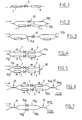
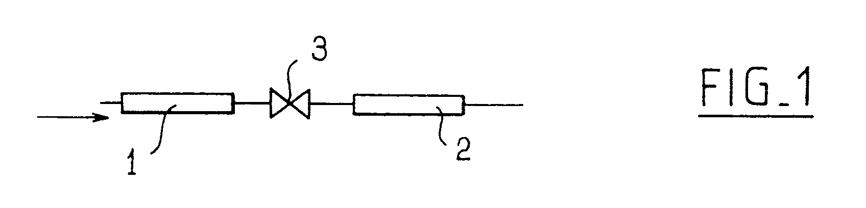
- phase modulator independent of the polarization illustrated in Figure 1 has two identical phase modulators 1 and 2 between which is placed a TE ⁇ TM converter referenced by 3.
- Modulators 1 and 2 are for example electro-optical modulators of the type which are described in detail below with reference to Figures 19 and following.
- the TM component is first modulated via the coefficient r33 in the first modulator, then is converted to TE polarization by the converter, then is modulated via the coefficient r13 in the second modulator.
- the incident TE component is modulated via the coefficient r13 in the first modulator, then is converted to TM polarization by the converter, then is modulated via the coefficient r33 in the second modulator. If the two modulators are the same length, the effect of modulation will be the same on both polarizations.
- FIGS 2 to 7 illustrate other variants of realization of the invention.
- the device illustrated in FIG. 2 is a intensity modulator of Mach-Zehnder type independent of polarization.
- One of its two branches, referenced by 21a, includes a mounting of the type illustrated on the figure 1.
- the other of its two branches, referenced by 21b, includes a TE ⁇ TM converter, referenced by 22.
- Figure 3 illustrates another embodiment possible for an intensity modulator insensitive to polarization.
- This modulator comprises two modulators 31a, 31b classic Mach-Zehnder type intensities which are mounted in series and between which is placed a TE ⁇ TM converter, referenced by 32.
- each of the two branches 41a, 41b of a Mach-Zehnder assembly can use on each of the two branches 41a, 41b of a Mach-Zehnder assembly, modulators of phase of the type illustrated in FIG. 1.
- the elementary modulators carry out modulations of phase of opposite signs.
- the Figure 1 modulator can be used on each of the two branches 51a, 51b of an intensity modulator at mirror (1/2 Mach-Zehnder of which each branch 51a, 51b is ends with a mirror 52), to make a "push-pull" mounting independent of polarization.
- the invention can be used to make directional couplers independent of the polarization.
- a Mach-Zehnder "push-pull" arrangement of the type shown in Figure 4 is disposed between two directional couplers 61, 62, both branches 63a, 63b of said assembly extending the branches of the output coupler 61 and extending through the input branches of the output coupler 62.
- the 3 dB directional couplers are of the type comprising two waveguides which are juxtaposed and extend parallel over part of their length.
- branches respectively of output and input of two directional couplers 71, 72 one input, one output, are connected by two branches 73a, 73b in each of which there is integrated a polarization converter 74a, 74b.
- the total variation of the coupling length for a given polarization is in this case the sum of variations in the coupling lengths of a coupler directive for each polarization.
- Figures 8 to 18 illustrate the characteristics of polarization of the different components that come to be described.
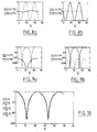
- the amplitude of the components TE and TM is expressed as a function of the phase shifts of the modulators 1 and 2 (identified by the indices 1 and 2), of the angle ⁇ 0 , and amplitudes of the waves before modulation:
- FIGS. 8a, 8b on which the amplitudes have been plotted modes depending on the applied modulation voltage to modulators 1 and 2.
- Mirror-type modulators are likely large-scale applications in an FTTH network.
- the insertion of a polarization converter in the arm of the modulator allows to make it insensitive to polarization. This is illustrated on Figures 15a, 15b and 16, when the arms contain two phase modulators in series with a TE converter ⁇ TM. It should be noted that in this case the optical wave crosses twice the converter and the output polarization is therefore identical to the input polarization. The effect push pull illustrated here lowers the tension of extinction.
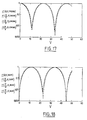
- FIG. 7 The behavior of an independent directional coupler of polarization (figure 7) is illustrated in the figures 17 and 18 on which we focused according to the modulation voltage, for CROSS and BAR states, total output intensity curves for different input polarization angles.
- the signal optic is incident in an arm of the coupler.
- the CROSS state corresponds to a cross: optical signal changes guide; while the BAR state corresponds to a signal remaining in the same optical guide.
- Figure 19 illustrates an example of a modulator capacitive according to the prior art. It includes a guide optics 101 which extends linearly and which is in one electrooptical material, as well as an electrode 102 which extends over part of the length of this light guide 101. This electrode 102 allows, with metallization earthed on the other side of the guide optic 1, to generate in said optical guide 101 a electric field for the modification of its index of refraction.
- an electrooptical modulator is characterized by the product V ⁇ L, where L is the optical path traveled by light, and V ⁇ is the half-wave voltage of the modulator, i.e. the voltage necessary to apply a phase shift of ⁇ to the light wave.
- V ⁇ L ⁇ .d not 3 .r eff , where ⁇ is the operating length, d the inter-electrode distance, n the refractive index of the core material, r eff the effective electrooptical coefficient.
- V ⁇ L ⁇ 0.16 Vm i.e., for an operating voltage of 10 V, an optical path of 1.6 cm.
- the length of the modulator must be at least greater than 1.6 cm, to an electrode width of 10 ⁇ m.
- FIG. 20 shows a modulator of phase according to a possible embodiment for the invention.
- the optical guide 111 of this modulator is folded twice on itself and has a looped shape lying down.
- the different portions of said modulator which extend juxtaposed at the level of said loop are overlapped by a metallization layer 12 which constitutes a modulator control electrode.
- a configuration of modulator of the type illustrated in FIG. 20 allows, for a given value of V ⁇ , to decrease considerably the length of the modulator.
- the modulator extends over 0.5 cm, for an optical length 1.6 cm total
- the width of the electrode 112 is 200 ⁇ m.
- Such a configuration with a folded optical guide can be used to reduce the value of V ⁇ for a fixed component size.
- the optical guide 131 is folded there in a pin hair.
- An electrode 132 is superimposed on two portions 131a and 131b juxtaposed with this optical guide 31.
- modulators which have just been described in reference to figures 20 to 22 are modulators capacitive used for command frequencies low (lower than a few GHz).
- control frequency bandwidth of such capacitive modulators is given by their constant RC, where R is their resistance and C their capacitance.
- FIG. 23 a modulator has been represented with traveling waves according to the invention.
- the optical guide 141 of this modulator is in loop.
- a metallization layer 142 is superimposed linearly to two parallel portions 141a and 141b of this optical guide 141. These portions 141a and 141b are such that the optical signal propagates there in the same direction.
- the metallization 142 is used as a transmission line for a microwave radio signal between an input ERf and an output S Rf , the input E Rf being connected to a microwave source.
- the optical signal propagates in the same direction in the two portions 141a and 141b.
- the meaning of propagation of the radio signal is the same as that of optical waves, so as to allow the agreement of phase between optical waves and microwave.
- the modulator thus constituted is a modulator with progressive waves.
- ⁇ loop is greater than ⁇ electrode .
- the bandwidth of a modulator traveling wave is reduced compared to that of a linear modulator, and is determined by the length of the loop.
- the interest of a wave modulator progressive loop is that the line microwave is shorter than for a modulator linear, and therefore there is less power dissipated in the modulator.
- the optical guide 151 of the modulators has a intermediate portion 151a which, on said optical guide 151, is interposed between two linear portions 151b and 151c of the same length covered by the same metallization 152, said intermediate portion 151a itself not being covered by this metallization 152.
- This intermediate portion 151a has a passive TE ⁇ TM converter 153 for example of the type of that described in the article already cited above.
- a first polarization of the optical signal is modulated during the passage thereof in the input branch 151b of the modulator.
- the polarization is reversed by the passive converter 153 when passing through the branch intermediate 151a and the second polarization is modulated during the second pass under the loop, that is to say during of the optical signal passing through the output branch 151c of the modulator.
- Such a modulator therefore has the advantage of allowing to modulate the two polarizations with a single electrode.
Landscapes
- Physics & Mathematics (AREA)
- Nonlinear Science (AREA)
- General Physics & Mathematics (AREA)
- Optics & Photonics (AREA)
- Engineering & Computer Science (AREA)
- Chemical & Material Sciences (AREA)
- Ceramic Engineering (AREA)
- Crystallography & Structural Chemistry (AREA)
- Microelectronics & Electronic Packaging (AREA)
- Optical Modulation, Optical Deflection, Nonlinear Optics, Optical Demodulation, Optical Logic Elements (AREA)
- Optical Integrated Circuits (AREA)
- Semiconductor Lasers (AREA)
Abstract
Description
- soit sur des matériaux optimisés (molécules de nature octupolaires orientées de manière non-centrosymétrique), mais les technologies envisagées ne sont pas encore opérationnelles,
- soit sur une succession d'électrodes qui modulent successivement les modes TE et TM.
- T. Gase, A. Braüer, W. Karthe, "Polarization insensitive phase modulator bases on polymers for hybrid integration", Proc. ECIO (Delft, Netherlands), 1995, S120.
et plus récemment, à
- la figure 1 est une représentation schématique d'un modulateur de phase insensible à la polarisation conforme à un mode de réalisation possible de l'invention ;
- les figures 2 à 5 sont des représentations schématiques de modulateurs d'intensité insensibles à la polarisation conformes à plusieurs modes de réalisations possibles de l'invention ;
- la figure 6 est une représentation schématique d'un coupleur 2x2 insensible à la polarisation ;
- la figure 7 est une représentation schématique d'un coupleur directif 2x2 insensible à la polarisation ;
- les figures 8a, 8b sont des graphes sur lesquels on a porté les amplitudes des modes en fonction de la tension de modulation appliquée aux modulateurs élémentaires du montage de la figure 1 ;
- les figures 9a, 9b sont des graphes sur lesquels on a porté les intensités des modes en fonction de la tension de modulation appliquée aux modulateurs élémentaires du montage de la figure 1 ;
- la figure 10 est un graphe sur lequel on a porté l'intensité totale en sortie du modulateur de la figure 2 pour différents angles de polarisation d'entrée, en fonction la tension de modulation ;
- les figures 11a, 11b et 12 sont des graphes analogues à ceux des figures 9a, 9b et 10, pour le modulateur de la figure 3 ;
- les figures 13a, 13b et 14 sont des graphes analogues à ceux des figures 9a, 9b et 10, pour le modulateur de la figure 4 ;
- les figures 15a, 15b et 16 sont des graphes analogues à ceux des figures 9a, 9b et 10, pour le modulateur de la figure 5 ;
- les figures 17 et 18 sont des graphes sur lesquels on a porté l'intensité totale en sortie d'un coupleur directif insensible à la polarisation, pour différents angles de polarisation d'entrée, en fonction de la tension de modulation, pour les signaux correspondant aux états CROSS et BAR du coupleur de la figure 7 ;
- la figure 19 illustre un modulateur conforme à un art antérieur connu ;
- les figures 20 à 25 illustrent des modulateurs conformes à différents modes de réalisation possibles pour l'invention.
- (M. C. Oh et al., Appl. Phys. Lett 67 (13) (1995) pp 1821-1823).


- J. Liang, R. Levenson, J. Zyss, ACS/OSA 93 (Toronto) - Topical Meeting - organic Thin Films for Photonic Applications, "Design and fabrication of electro-optic polymer waveguides".
et où τboucle et τélectrode désignent respectivement les retards optiques dus à la boucle et à l'électrode,
Claims (15)
- Composant optique du type comportant un guide optique dont le coeur est en un matériau électrooptique, caractérisé en ce qu'il comporte un convertisseur (3, 32) TE TM entre deux modulateurs électrooptiques (1, 2 ; 31a, 31b).
- Composant selon la revendication 1, caractérisé en ce que les modulateurs (1, 2) sont des modulateurs de phase.
- Composant selon la revendication 2, caractérisé en ce qu'il comporte une structure Mach-Zehnder dont une branche (21b) comporte un convertisseur (22) TE TM et dont l'autre branche (21a) comporte deux modulateurs de phase (1, 2) entre lesquels sont interposés un convertisseur (3) TE TM.
- Composant selon la revendication 1, caractérisé en ce qu'il comporte deux modulateurs d'intensité (31a, 31b) de type Mach-Zehnder entre lesquels sont interposés un convertisseur (32) TE TM.
- Composant selon la revendication 1, caractérisé en ce qu'il comporte un modulateur d'intensité de type Mach-Zehnder dont chaque branche (41a, 41b ; 51a, 51b ; 63a, 63b) comporte deux modulateurs de phase (1, 2) entre lesquels est interposé un convertisseur (3) TE TM, les modulations de phase réalisées par les modulateurs de chacune des deux branches étant de signes opposés.
- Composant selon la revendication 5, caractérisé en ce que le modulateur d'intensité est un 1/2 Mach-Zehnder à miroir (s).
- Composant selon la revendication 5, caractérisé à ce qu'à leurs extrémités, les branches du montage Mach-Zehnder sont reliées aux branches de deux coupleurs directifs (61, 62).
- Composant optique comportant un guide optique dont le coeur est en un matériau électrooptique, caractérisé en ce qu'il comporte deux coupleurs directifs (71, 72), l'un d'entrée, l'autre de sortie, les branches de sortie du coupleur d'entrée (71) et les branches d'entrée du coupleur de sortie (72) étant reliées par deux branches (73a, 73b) qui comportent chacune un convertisseur (74a, 74b) TE TM.
- Composant optique comportant un guide optique (111, 121, 131, 141, 151) dont le coeur est en un matériau électrooptique, ainsi qu'au moins une métallisation (112, 122, 132, 142, 152) au droit d'une portion dudit guide, pour la commande de celui-ci, caractérisé en ce que le guide optique (111, 121, 131, 141, 151) est replié et en ce que la métallisation (112, 122, 132, 142, 152) s'étend au droit d'au moins deux portions du guide optique qui s'étendent de façon repliée l'une par rapport à l'autre.
- Composant selon la revendication 9, caractérisé en ce que le matériau électrooptique est un matériau polymère.
- Composant capacitif selon l'une des revendications 9 ou 10, caractérisé en ce que la métallisation (112, 122, 132, 152) est une électrode de commande dudit composant.
- Composant à ondes progressives selon l'une des revendications 9 ou 10, caractérisé en ce que la métallisation (142, 152) est une ligne de transmission hyperfréquence et en ce que le signal optique se propage dans les portions (141, 141b ; 151b, 151c) de guide au droit desquelles ladite métallisation (142, 152) s'étend, dans la même direction et le même sens que le signal hyperfréquence qui se propage dans cette métallisation.
- Composant selon l'une des revendications 9 à 12, caractérisé en ce que le guide optique (151) comporte un convertisseur de polarisation (153) entre deux portions (151b, 151c) au droit desquelles s'étend la métallisation de commande (152).
- Composant de modulation selon l'une des revendications 9 à 12.
- Composant de commutation selon l'une des revendications 9 à 12.
Applications Claiming Priority (2)
| Application Number | Priority Date | Filing Date | Title |
|---|---|---|---|
| FR9607528A FR2749945B1 (fr) | 1996-06-18 | 1996-06-18 | Composant electrooptique |
| FR9607528 | 1996-06-18 |
Publications (3)
| Publication Number | Publication Date |
|---|---|
| EP0816896A2 true EP0816896A2 (fr) | 1998-01-07 |
| EP0816896A3 EP0816896A3 (fr) | 1998-02-11 |
| EP0816896B1 EP0816896B1 (fr) | 2004-08-25 |
Family
ID=9493137
Family Applications (1)
| Application Number | Title | Priority Date | Filing Date |
|---|---|---|---|
| EP97401380A Expired - Lifetime EP0816896B1 (fr) | 1996-06-18 | 1997-06-17 | Composant électrooptique |
Country Status (4)
| Country | Link |
|---|---|
| US (1) | US5930412A (fr) |
| EP (1) | EP0816896B1 (fr) |
| DE (1) | DE69730384T2 (fr) |
| FR (1) | FR2749945B1 (fr) |
Cited By (2)
| Publication number | Priority date | Publication date | Assignee | Title |
|---|---|---|---|---|
| US6148122A (en) * | 1998-11-17 | 2000-11-14 | Qtera Corporation | High speed lithium niobate polarization independent modulators |
| EP1109051A1 (fr) * | 1999-12-06 | 2001-06-20 | Qtera Corporation | Modulateur de phase optique indépendant de la polarisation |
Families Citing this family (10)
| Publication number | Priority date | Publication date | Assignee | Title |
|---|---|---|---|---|
| FR2776784A1 (fr) * | 1998-03-30 | 1999-10-01 | France Telecom | Modulateur electro-optique integre hybride du type a effet pockels |
| US6337755B1 (en) * | 1998-11-17 | 2002-01-08 | Qtera Corporation | Polarization independent all-optical regenerators |
| AU2903101A (en) * | 1999-09-21 | 2001-04-30 | Nanovation Technologies, Inc. | A nanophotonic mach-zehnder interferometer switch and filter |
| EP1107488A1 (fr) * | 1999-12-06 | 2001-06-13 | Qtera Corporation | Régénérateur optique indépendent de la polarisation |
| US6512860B2 (en) * | 2000-08-18 | 2003-01-28 | Danmarks Tekniske Universitet | Bent electro-absorption modulator |
| US6760493B2 (en) * | 2001-06-28 | 2004-07-06 | Avanex Corporation | Coplanar integrated optical waveguide electro-optical modulator |
| EP1271220B1 (fr) * | 2001-06-28 | 2009-08-12 | Avanex Corporation | Modulateur électro-optique avec un guide d'onde optique coplanaire intégré |
| US6754429B2 (en) * | 2001-07-06 | 2004-06-22 | Corning Incorporated | Method of making optical fiber devices and devices thereof |
| EP1279999A1 (fr) * | 2001-07-23 | 2003-01-29 | Corning Incorporated | Atténuateur optique variable insensible à la polarisation |
| US8173045B2 (en) | 2008-05-28 | 2012-05-08 | University Of Washington | Diels-Alder crosslinkable dendritic nonlinear optic chromophores and polymer composites |
Family Cites Families (11)
| Publication number | Priority date | Publication date | Assignee | Title |
|---|---|---|---|---|
| US3589794A (en) * | 1968-08-07 | 1971-06-29 | Bell Telephone Labor Inc | Optical circuits |
| US4384760A (en) * | 1980-12-15 | 1983-05-24 | Bell Telephone Laboratories, Incorporated | Polarization transformer |
| US4390236A (en) * | 1981-03-19 | 1983-06-28 | Bell Telephone Laboratories, Incorporated | Tunable polarization independent wavelength filter |
| US4691984A (en) * | 1985-09-26 | 1987-09-08 | Trw Inc. | Wavelength-independent polarization converter |
| GB8630959D0 (en) * | 1986-12-29 | 1987-02-04 | British Telecomm | Optical polarisation control |
| NL9200576A (nl) * | 1992-03-27 | 1993-10-18 | Nederland Ptt | Regelbare polarisatie-omvormer. |
| JP2724098B2 (ja) * | 1992-10-07 | 1998-03-09 | 沖電気工業株式会社 | 光波長フィルタ装置 |
| JPH07159738A (ja) * | 1993-12-06 | 1995-06-23 | Hitachi Chem Co Ltd | アクティブ光導波路用組成物、これを用いたアクティブ光導波路の製造法及びアクティブ光導波路 |
| DE19549395A1 (de) * | 1995-02-07 | 1996-10-31 | Ldt Gmbh & Co | Bilderzeugungssysteme zur Bestimmung von Sehfehlern an Probanden und für deren Therapie |
| NL1003198C2 (nl) * | 1995-07-07 | 1997-11-25 | Nederland Ptt | Polarisatie-onafhankelijke optische inrichting. |
| US5654818A (en) * | 1996-02-09 | 1997-08-05 | The United States Of America As Represented By The United States National Aeronautics And Space Administration | Polarization independent electro-optic modulator |
-
1996
- 1996-06-18 FR FR9607528A patent/FR2749945B1/fr not_active Expired - Fee Related
-
1997
- 1997-06-17 DE DE69730384T patent/DE69730384T2/de not_active Expired - Lifetime
- 1997-06-17 EP EP97401380A patent/EP0816896B1/fr not_active Expired - Lifetime
- 1997-06-18 US US08/878,048 patent/US5930412A/en not_active Expired - Lifetime
Cited By (2)
| Publication number | Priority date | Publication date | Assignee | Title |
|---|---|---|---|---|
| US6148122A (en) * | 1998-11-17 | 2000-11-14 | Qtera Corporation | High speed lithium niobate polarization independent modulators |
| EP1109051A1 (fr) * | 1999-12-06 | 2001-06-20 | Qtera Corporation | Modulateur de phase optique indépendant de la polarisation |
Also Published As
| Publication number | Publication date |
|---|---|
| DE69730384T2 (de) | 2005-09-01 |
| US5930412A (en) | 1999-07-27 |
| FR2749945B1 (fr) | 1998-09-11 |
| EP0816896B1 (fr) | 2004-08-25 |
| EP0816896A3 (fr) | 1998-02-11 |
| FR2749945A1 (fr) | 1997-12-19 |
| DE69730384D1 (de) | 2004-09-30 |
Similar Documents
| Publication | Publication Date | Title |
|---|---|---|
| EP0442802B1 (fr) | Séparateur de polarisations pour lumière guidée | |
| US10481463B2 (en) | All optical fast fourier transform on chip with heating tunability design, simulation, fabrication, and performance analysis | |
| EP0017571B1 (fr) | Modulateur d'intensité lumineuse en optique intégrée et circuit optique intégré comportant un tel modulateur | |
| EP0816896B1 (fr) | Composant électrooptique | |
| EP0050059A1 (fr) | Jonction optique hybride et application à un dispositif interférométrique en anneau | |
| EP0788017B1 (fr) | Miroir optique non linéaire en boucle (NOLM) indépendant de la polarisation | |
| WO2020074834A2 (fr) | Interféromètre de sagnac à fibre optique compact | |
| FR2695216A1 (fr) | Commutateur optique ayant une direction de propagation proche de l'axe Z du matériau électro-optique. | |
| EP0869377B1 (fr) | Composant d'optique intégrée avec effet de polarisation | |
| EP1433017A2 (fr) | Modulateur electro-optique, procede de realisation et bloc pour mise en oeuvre | |
| EP0099282B1 (fr) | Dispositif optique intégré modulateur indépendant de la polarisation incidente | |
| CN100353213C (zh) | 用于在光学器件中相移光束的方法和设备 | |
| EP0094866B1 (fr) | Dispositif de liaison conversationnelle de type BUS à fibres optiques unimodales | |
| US20090214150A1 (en) | Integrated polarization splitter/combiner | |
| EP0783127B1 (fr) | Coupleur interférométrique Mach-Zehnder à fibre optique monomode | |
| EP0125182B1 (fr) | Coupleur directif électro-optique à trois électrodes et à déphasage alterne | |
| EP0795778A1 (fr) | Dispositif optique non-linéaire de traitement de signaux optiques | |
| Gill et al. | Optical modulation techniques for analog signal processing and CMOS compatible electro-optic modulation | |
| Mokeddem | Polarization control devices in silicon photonics | |
| Moss | Minimizing experimental sourced errors for microwave photonic signal processors based on integrated microcombs | |
| WO2024002925A1 (fr) | Procédé et dispositif de filtrage optique à réponse impulsionnelle finie et équipements optiques correspondants | |
| Baba | Recent progress in on-chip slow light devices | |
| Salon | Silicon Based Optoelectronic Technology | |
| FR2856155A1 (fr) | Circuit optique integre comportant au moins une jonction de guide de lumiere en y notamment pour gyrometre a fibre optique. | |
| EP1775608A1 (fr) | Polariseur compact et séparateur de polarisation associé pour dispositifs à semi-conducteurs |
Legal Events
| Date | Code | Title | Description |
|---|---|---|---|
| PUAI | Public reference made under article 153(3) epc to a published international application that has entered the european phase |
Free format text: ORIGINAL CODE: 0009012 |
|
| PUAL | Search report despatched |
Free format text: ORIGINAL CODE: 0009013 |
|
| AK | Designated contracting states |
Kind code of ref document: A2 Designated state(s): DE FR GB |
|
| AK | Designated contracting states |
Kind code of ref document: A3 Designated state(s): AT BE CH DE DK ES FI FR GB GR IE IT LI LU MC NL PT SE |
|
| 17P | Request for examination filed |
Effective date: 19980803 |
|
| AKX | Designation fees paid |
Free format text: DE FR GB |
|
| RBV | Designated contracting states (corrected) |
Designated state(s): DE FR GB |
|
| 17Q | First examination report despatched |
Effective date: 20030725 |
|
| GRAP | Despatch of communication of intention to grant a patent |
Free format text: ORIGINAL CODE: EPIDOSNIGR1 |
|
| GRAS | Grant fee paid |
Free format text: ORIGINAL CODE: EPIDOSNIGR3 |
|
| GRAA | (expected) grant |
Free format text: ORIGINAL CODE: 0009210 |
|
| AK | Designated contracting states |
Kind code of ref document: B1 Designated state(s): DE FR GB |
|
| REG | Reference to a national code |
Ref country code: GB Ref legal event code: FG4D Free format text: NOT ENGLISH |
|
| GBT | Gb: translation of ep patent filed (gb section 77(6)(a)/1977) |
Effective date: 20040818 |
|
| REF | Corresponds to: |
Ref document number: 69730384 Country of ref document: DE Date of ref document: 20040930 Kind code of ref document: P |
|
| PLBE | No opposition filed within time limit |
Free format text: ORIGINAL CODE: 0009261 |
|
| STAA | Information on the status of an ep patent application or granted ep patent |
Free format text: STATUS: NO OPPOSITION FILED WITHIN TIME LIMIT |
|
| 26N | No opposition filed |
Effective date: 20050526 |
|
| REG | Reference to a national code |
Ref country code: GB Ref legal event code: 732E Free format text: REGISTERED BETWEEN 20090528 AND 20090603 |
|
| REG | Reference to a national code |
Ref country code: FR Ref legal event code: TP |
|
| PGFP | Annual fee paid to national office [announced via postgrant information from national office to epo] |
Ref country code: DE Payment date: 20110630 Year of fee payment: 15 |
|
| PGFP | Annual fee paid to national office [announced via postgrant information from national office to epo] |
Ref country code: FR Payment date: 20120614 Year of fee payment: 16 |
|
| REG | Reference to a national code |
Ref country code: DE Ref legal event code: R119 Ref document number: 69730384 Country of ref document: DE Effective date: 20130101 |
|
| PG25 | Lapsed in a contracting state [announced via postgrant information from national office to epo] |
Ref country code: DE Free format text: LAPSE BECAUSE OF NON-PAYMENT OF DUE FEES Effective date: 20130101 |
|
| REG | Reference to a national code |
Ref country code: FR Ref legal event code: ST Effective date: 20140228 |
|
| PG25 | Lapsed in a contracting state [announced via postgrant information from national office to epo] |
Ref country code: FR Free format text: LAPSE BECAUSE OF NON-PAYMENT OF DUE FEES Effective date: 20130701 |
|
| PGFP | Annual fee paid to national office [announced via postgrant information from national office to epo] |
Ref country code: GB Payment date: 20140527 Year of fee payment: 18 |
|
| GBPC | Gb: european patent ceased through non-payment of renewal fee |
Effective date: 20150617 |
|
| PG25 | Lapsed in a contracting state [announced via postgrant information from national office to epo] |
Ref country code: GB Free format text: LAPSE BECAUSE OF NON-PAYMENT OF DUE FEES Effective date: 20150617 |