EP0816977B1 - Verbindung eines Doppelspannungsmoduls - Google Patents
Verbindung eines Doppelspannungsmoduls Download PDFInfo
- Publication number
- EP0816977B1 EP0816977B1 EP97110770A EP97110770A EP0816977B1 EP 0816977 B1 EP0816977 B1 EP 0816977B1 EP 97110770 A EP97110770 A EP 97110770A EP 97110770 A EP97110770 A EP 97110770A EP 0816977 B1 EP0816977 B1 EP 0816977B1
- Authority
- EP
- European Patent Office
- Prior art keywords
- pins
- voltage
- component card
- card
- ground
- Prior art date
- Legal status (The legal status is an assumption and is not a legal conclusion. Google has not performed a legal analysis and makes no representation as to the accuracy of the status listed.)
- Expired - Lifetime
Links
Images

Classifications
-
- G—PHYSICS
- G06—COMPUTING OR CALCULATING; COUNTING
- G06F—ELECTRIC DIGITAL DATA PROCESSING
- G06F1/00—Details not covered by groups G06F3/00 - G06F13/00 and G06F21/00
- G06F1/16—Constructional details or arrangements
- G06F1/18—Packaging or power distribution
- G06F1/189—Power distribution
-
- G—PHYSICS
- G06—COMPUTING OR CALCULATING; COUNTING
- G06F—ELECTRIC DIGITAL DATA PROCESSING
- G06F13/00—Interconnection of, or transfer of information or other signals between, memories, input/output devices or central processing units
- G06F13/38—Information transfer, e.g. on bus
- G06F13/40—Bus structure
- G06F13/4063—Device-to-bus coupling
- G06F13/409—Mechanical coupling
Definitions
- the present invention relates to the field of computer systems. More particularly, the present invention relates to the field of component cards inserted into buses of computer systems.
- Computer systems and computer components are being developed to operate using lower and lower voltages. It is currently typical for older systems to operate with 5 volts and for newer systems to operate with 3.3 volts. As systems are developed to operate with lower voltages, problems of compatibility between systems and add-on components can occur. For example, a purchaser of a new system using a lower voltage than the old one may wish to continue using add-on memory modules from the old system because buying new memory modules would be expensive. Even though 3.3 volt systems are able to supply both 3.3 and 5 volts to components, current 3.3 volt systems incur difficulties when using previous, 5 volt components.
- US-5,272,664 discloses a single in-line module (SIMM) for use in a computer memory board.
- the SIMM can comprise components having either 3.3 or 5 volt power supply requirements. For conveying 3.3 volt power dedicated 3.3 volt pins or for supplying 5 volt power dedicated 5 volt pins are arranged on a connector of the SIMM. Although different power supply levels are contemplated, use of a SIMM for operating with both power supplies is not disclosed.
- ground pins are provided which can be use either in case of a 3.3 volt power supply or a 5 volt power supply.
- the power supply pins, the ground pins and pins for conveying signals to the SIMM are interspersed with each other, forming a continuous series of consecutive pins. In this series, the 3.3 and 5 volt power supply pins are arranged symmetrically. In particular, the pin arrangement does not include separated portions wherein each of the portions includes power pins for supplying only 3.3 or 5 volt and associated ground pins.
- EP 0 692 927 A2 is directed to printed circuit boards (PCBs) operated at two different supply voltage levels wherein it is necessary to decouple voltage pins for one supply voltage level to ground and to provide for an alternating current return path for these pins.
- EP 0 692 927 A2 is directed to the problem to decouple 3.3 volt pins of a PCB from ground to provide an alternating current return path.
- a PCB is provided which includes a metal layer being divided in two electrically isolated sections. One of the electrically isolated sections is associated to a 5 volt power supply while the other electrically isolated section is associated to a 3.3 volt power supply. The electrically isolated section associated to the 3.3 volt power supply is coupled to respective signal pins.
- capacitors are coupled between the signal pins and the electrically isolated section associated to the 3.3 volt power supply on one hand and to the electrically isolated section associated to the 5 volt power supply on the other hand.
- an alternating current return path is provided with respect to the signal pins coupled to the electrically isolated section associated to the 3.3 volt power supply.
- this capacitors do not provide for a storage of the 5 volt voltage level.
- the present invention provides an apparatus according to claim 1.
- the present invention operates in a computer system supplying both a higher voltage and a lower voltage to system components, for example 5 volts and 3.3 volts.
- the component card of the present invention can include 5 volt integrated circuits (ICs) or 3.3 volt ICs. When 5 volt ICs are used, however, other components of the system receiving signals from the component card should be 5 volt input/output (I/O) tolerant to avoid damage to the other components.
- I/O input/output
- a 3.3 volt memory controller communicating with the component card should be capable of receiving signals at a higher voltage than 3.3 volts without damage.
- FIG. 1 is a block diagram of a portion 100 of a computer system of the present invention.
- Portion 100 includes memory bus 102.
- Processor 104 and main memory 108 are coupled to memory bus 102.
- Processor 104 accesses data from main memory 104 through memory bus 102.
- Main memory 108 includes random access memory (RAM).
- RAM is in the form of component cards or modules which contain IC RAMs and attach to memory bus 108 at interconnect 120. Component cards and interconnects will be described more fully below. In other embodiments, additional components could be coupled to memory bus 102.
- Bus adapter 106 coupled to memory bus 102 and I/O bus 110 performs functions that allow the transfer of data between the two buses. For example, bus adapter 106 controls "traffic" between the buses to prevent data collisions.
- I/O bus 110 transfers data entering or exiting portion 100 from and to network bus 118.
- Network bus 118 connects to different processors in the computer system.
- I/O controllers 112 and 116 are examples of types of I/O controllers attachable to I/O bus 110 for facilitating specific types of communication between portion 100 and devices exterior to portion 100.
- I/O controller 112 is a graphics controller receiving data from processor 104 and producing graphics output 114.
- I/O controller 116 is a network controller managing communications between network bus 118 and I/O bus 110.
- I/O controllers 112 and 116 are component cards including ICs performing the appropriate functions. Other embodiments could include additional I/O controllers. Controllers 112 and 116 attach to I/O bus 110 at interconnects 120 as shown.
- Computer system portion 100 is physically embodied in a printed circuit board (not shown) comprising ICs coupled to the proper circuit traces, or paths, on the printed circuit board.
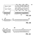
- FIG. 2A shows a simplified illustration 200 of an embodiment of dual voltage component card 202 of the present invention.
- dual voltage component card 202 is a memory component card, or memory module. It will be apparent to one of ordinary skill in the art that other types of functionality may be supported on such a card.
- a component card like component card 202 could be a network card or a graphics card.
- FIG. 2B shows an end view 240 of component card 202.
- FIG. 2C is a simplified illustration of an embodiment 260 of a dual voltage component card socket capable of receiving component card 202.
- Component card 202 includes pin groups 204 and 206, where pin 208 is called out for example. Pin 208 is identical physically to all other pins in pin groups 204 and 206, but various pins are used for different functions. Pin groups 204 and 206 and socket 260 make up interconnect 120.
- pin 208 is formed by depositing a highly conductive material, for example gold, onto component card 202.
- the distance between pins in pin groups 204 and 206 is not indicative of actual pin placement, but is so shown for illustration. The actual configuration of the pins themselves and the distance between them, for this embodiment, is standard and well known for conventional component cards.
- the number of pins shown in pin groups 204 and 206 is less than an actual number of pins typically used in the preferred embodiment. While the exact number of pins in each group can vary, an embodiment of the invention uses 32 pins in group 204 and 200 pins in group 206.
- IC RAMs 212a-212h are attached to component card 202 so that pins of the RAMs electrically connect to circuit paths of component card 202.
- the circuit paths communicate with pin groups 204 and 206.
- Pin group 204 comprises pins for power and ground.
- Pin group 206 comprises pins for power, ground and signal, where signal can be any kind of information signal sent or received by the RAMs, for example, signals for data, address or control.
- the power voltage for pin group 204 is lower than the power voltage for pin group 206. For this embodiment, the lower voltage is 3.3 volts and the higher voltage is 5 volts.
- Component card 202 can be used with 5 volt RAMs 212a-212h or with 3.3 volt RAMs 212a-212h.
- pin group 204 provides ground and power for RAMs 212a-212h and pin group 206 provides signal pins.
- power and ground are provided as described below. Because the distance traveled by the power signals is large relative to, for example, the distance between pins 206 and RAMs 212a-212h, a possibility of voltage droop exists.
- capacitors 210a-210d are provided. Capacitors 210a-210d are connected between power pins of pins 204 and power pins of RAMs 212a-212h to sustain the lower voltage level provided via pin group 204, thereby alleviating voltage droop.
- capacitors 210e-210l are connected through one terminal to a 5 volt pin of pin group 206 and through the other terminal to a ground pin of pin group 206. This provides a ground return for 5 volt signals on power pins of pin group 206 when 3.3 volt RAMs 212a-212h are used, thereby alleviating ground bounce and crosstalk.
- component card 202 When component card 202 is used with 5 volt RAMs 212a-212h, voltage, ground and signal are all supplied to RAMs 212a-212h by pins 206. In this situation, pins 204 and capacitors 210a-210d are not used.
- FIG. 2B shows end view 240 of component card 202.
- component card 202 is a dual in-line memory module (DIMM). Dual in-line modules, or component cards, have row of pins on each side of the component card to allow for the receipt and transmission of more signals.
- component card 202 could be a single in-line memory module (SIMM), with pins on only one side.
- FIG. 2C shows a simplified illustration of an end view of an embodiment 260 of a dual voltage component card socket of the present invention.
- FIG. 2C shows the end of socket 260 into which component card 202 is installed.
- the opposite end of socket 260 (not shown) is electrically coupled to a printed circuit board in the computer system of portion 100.
- Socket 260 includes lower voltage section 218 and higher voltage section 220.
- the lower voltage is 3.3 volts and the higher voltage is 5 volts.
- Section 218 includes housing 228 and connector area 222. 16 connectors are shown in connector area 222 for contacting pins of pin group 204 when component card 202 is inserted into socket 260.
- pin 208 contacts connector 226.
- Opposite ends of connectors in connector area 222 are electrically coupled to appropriate circuit paths on the printed circuit board, for example, by soldering or friction coupling.
- connectors of connector area 222 are coupled to ground and 3.3 volt paths.
- 5 volt section 220 includes housing 230 and connector area 224. Section 220 functions with component card 202 as described with respect to section 218. The connectors of connection area 224, however, are coupled to ground, 5 volt, and signal paths of the printed circuit board.
Landscapes
- Engineering & Computer Science (AREA)
- Theoretical Computer Science (AREA)
- General Engineering & Computer Science (AREA)
- Physics & Mathematics (AREA)
- General Physics & Mathematics (AREA)
- Power Engineering (AREA)
- Human Computer Interaction (AREA)
- Computer Hardware Design (AREA)
- Techniques For Improving Reliability Of Storages (AREA)
- Power Sources (AREA)
- Details Of Connecting Devices For Male And Female Coupling (AREA)
- Memory System (AREA)
- Coupling Device And Connection With Printed Circuit (AREA)
Claims (15)
- Eine Komponentenkartenverbindungsvorrichtung zum Verbinden einer Komponentenkarte mit einem eine Komponentenkarte umfassenden Computersystem, mit:einem ersten Bereich mit einer ersten Gruppe in Reihe angeordneter Kontaktstifte (206) mit ersten Leistungsstiften zur Übertragung einer ersten Spannung, ersten Massestiften zur Übertragung von Masse und Signalstiften zur Übertragung von Signalen, die Komponenten auf der Komponentenkarte (202) zuzuführen sind,einem zweiten Bereich mit einer zweiten Gruppe in Reihe angeordneter Kontaktstifte (204) mit zweiten Leistungsstiften zur Übertragung einer zweiten Spannung, die kleiner als die erste Spannung ist, und zweiten Massestiften zur Übertragung von Masse,wobei der erste Bereich und der zweite Bereich voneinander getrennt sind, undwobei die erste oder die zweite Spannung zu einem Zeitpunkt zu Komponenten (212) auf der Komponentenkarte (202) übertragen wird,ersten Kapazitäten (201e-I), die mit den ersten Leitungsstiften und mit den ersten Massestiften verbunden sind, um der ersten Spannung eine Masserückleitung bereitzustellen, wenn die zweite Spannung von den Komponenten (212) empfangen wird,zweiten Kapazitäten (210a-d), die mit den zweiten Leistungsstiften verbunden sind, um die zweite Spannung zur Verwendung von Komponenten (212) auf der Komponentenkarte (202) zu speichern, undeinem Stecksockel (260) mit:einem ersten Anschlussbereich (220) zur Aufnahme der ersten Gruppe in Reihe angeordneter Kontaktstifte (206) und zur Übertragung der ersten Spannung und Masse, undeinem zweiten Anschlussbereich (218) zur Aufnahme der zweiten Gruppe in Reihe angeordneter Kontaktstifte (204) und zur Übertragung der zweiten Spannung und Masse,wobei der erste Anschlussbereich (220) und der zweite Anschlussbereich (218) voneinander getrennt sind.
- Die Komponentenkartenverbindungsvorrichtung nach Anspruch 1, bei der die ersten und zweiten Gruppen in Reihe angeordneter Kontaktstifte (106, 104) in parallelen Reihen angeordnete Kontaktstifte sind.
- Die Komponentenkartenverbindung nach Anspruch 1, bei der die ersten und zweiten Gruppen von Kontaktstiften (106, 104) in einer Reihe angeordnete Einzelkontaktstifte sind.
- Die Komponentenkartenverbindungsvorrichtung nach Anspruch 2, bei der die Komponentenkarte (202) ein mit in parallelen Reihen angeordneten Anschlüssen versehenes Speichermodul (DIMM) ist.
- Die Komponentenkartenverbindungsvorrichtung aus Anspruch 3, bei der die Komponentenkarte (302) ein mit in einer Reihe angeordneten Anschlüssen versehenes Speichermodul (SIMM) ist.
- Die Komponentenkartenverbindungsvorrichtung nach einem der Ansprüche 1 bis 5, die so mit der ersten und der zweiten Spannung und mit Masse verbunden ist, dass die erste Spannung an die ersten Leistungskontaktstifte angelegt ist und die zweite Spannung an die zweiten Leistungskontaktstifte angelegt ist und dass Masse an die ersten und zweiten Massekontaktstifte angelegt ist.
- Die Komponentenkartenvorrichtung nach einem der Ansprüche 1 bis 6, die von einem Computersystem umfasst ist, das eine erste Spannung und eine zweite Spannung zu Komponenten des System zu verteilen vermag.
- Die Komponentenkartenverbindungsvorrichtung nach einem der Ansprüche 1 bis 6, das von einem Computersystem umfasst ist, das Komponenten, die bei einer ersten Spannung arbeiten, und Komponenten umfasst, die bei einer zweiten Spannung arbeiten, wobei das Computersystem ferner umfasst:einen Speicherbus (102),einen Eingabe/Ausgabe-(I/0)-Bus (110),einen Netzwerkbus (118),einen Prozessor (104), der mit dem Speicherbus (102) verbunden ist,ein mit dem Speicherbus verbundenes Speichersystem, das einen Hauptspeicher (108) und einen Speicher mit wahlfreiem Zugriff (RAM) umfasst, undeine I/O-Vorrichtung, die mit dem I/O-Bus (110) und mit dem Netzwerkbus (108) verbunden ist, um Kommunikation zwischen dem I/O-Bus (110) und dem Netzwerkbus (118) zu steuern.
- Die Komponentenkartenverbindungsvorrichtung nach Anspruch 8, die mit dem Speicherbus (102) verbunden ist und bei der die Komponentenkarte (202) ein mit in parallelen Reihen angeordneten Anschlüssen versehenes Speichermodul (DIMM) umfasst, das den RAM umfasst.
- Die Komponentenkartenverbindungsvorrichtung nach Anspruch 8, die mit dem Speicherbus (102) verbunden ist und bei der die Komponentenkarte (202) ein mit in einer Reihe angeordneten Anschlüssen versehenes Speichermodul (SIMM) umfasst, das den RAM umfasst.
- Die Komponentenkartenverbindungsvorrichtung nach Anspruch 8, die dem Speicherbus (102) verbunden ist und bei der die Komponentenkarte (202) eine I/O-Karte umfasst, die die I/O-Vorrichtung umfasst.
- Die Komponentenkartenverbindungsvorrichtung nach Anspruch 11, bei der die I/O-Karte eine Netzwerk-I/O-Steuerkarte (112, 116) ist.
- Die Komponentenkartenverbindungsvorrichtung nach Anspruch 11, bei der die I/O-Karte eine Graphikkarte (114) ist.
- Die Komponentenkartenverbindungsvorrichtung nach einem der Ansprüche 1 bis 13, bei der die erste Spannung 5 Volt beträgt und die zweite Spannung 3,3 Volt beträgt.
- Die Komponentenkartenverbindungsvorrichtung nach einem der Ansprüche 1 bis 14, bei der die zu Komponenten (212) auf der Komponentenkarte (202) zuzuführenden Signale, immer über die Signalkontaktstifte der ersten Gruppe von in Reihe angeordneten Kontaktstiften (206) übertragen werden.
Applications Claiming Priority (2)
| Application Number | Priority Date | Filing Date | Title |
|---|---|---|---|
| US08/675,256 US5758100A (en) | 1996-07-01 | 1996-07-01 | Dual voltage module interconnect |
| US675256 | 1996-07-01 |
Publications (3)
| Publication Number | Publication Date |
|---|---|
| EP0816977A2 EP0816977A2 (de) | 1998-01-07 |
| EP0816977A3 EP0816977A3 (de) | 1999-03-24 |
| EP0816977B1 true EP0816977B1 (de) | 2003-10-15 |
Family
ID=24709696
Family Applications (1)
| Application Number | Title | Priority Date | Filing Date |
|---|---|---|---|
| EP97110770A Expired - Lifetime EP0816977B1 (de) | 1996-07-01 | 1997-07-01 | Verbindung eines Doppelspannungsmoduls |
Country Status (5)
| Country | Link |
|---|---|
| US (1) | US5758100A (de) |
| EP (1) | EP0816977B1 (de) |
| JP (1) | JPH113147A (de) |
| KR (1) | KR980010693A (de) |
| DE (2) | DE69725519T2 (de) |
Families Citing this family (38)
| Publication number | Priority date | Publication date | Assignee | Title |
|---|---|---|---|---|
| US6728851B1 (en) * | 1995-07-31 | 2004-04-27 | Lexar Media, Inc. | Increasing the memory performance of flash memory devices by writing sectors simultaneously to multiple flash memory devices |
| US8171203B2 (en) * | 1995-07-31 | 2012-05-01 | Micron Technology, Inc. | Faster write operations to nonvolatile memory using FSInfo sector manipulation |
| US6978342B1 (en) | 1995-07-31 | 2005-12-20 | Lexar Media, Inc. | Moving sectors within a block of information in a flash memory mass storage architecture |
| US5845313A (en) | 1995-07-31 | 1998-12-01 | Lexar | Direct logical block addressing flash memory mass storage architecture |
| US5911050A (en) * | 1997-07-01 | 1999-06-08 | International Business Machines Corporation | System for connecting either of two supply voltage type PCI cards using a common connector socket |
| US6108228A (en) * | 1997-12-02 | 2000-08-22 | Micron Technology, Inc. | Quad in-line memory module |
| US7102671B1 (en) | 2000-02-08 | 2006-09-05 | Lexar Media, Inc. | Enhanced compact flash memory card |
| AU7692701A (en) * | 2000-07-20 | 2002-02-05 | Rlx Technologies Inc | Single board web server system and method |
| US6757748B1 (en) | 2000-07-20 | 2004-06-29 | Rlx Technologies, Inc. | Modular network interface system and method |
| US6747878B1 (en) | 2000-07-20 | 2004-06-08 | Rlx Technologies, Inc. | Data I/O management system and method |
| US6985967B1 (en) | 2000-07-20 | 2006-01-10 | Rlx Technologies, Inc. | Web server network system and method |
| US7167944B1 (en) | 2000-07-21 | 2007-01-23 | Lexar Media, Inc. | Block management for mass storage |
| JP2002324393A (ja) * | 2001-04-25 | 2002-11-08 | Mitsubishi Electric Corp | 半導体記憶装置 |
| GB0123417D0 (en) * | 2001-09-28 | 2001-11-21 | Memquest Ltd | Improved data processing |
| GB0123410D0 (en) | 2001-09-28 | 2001-11-21 | Memquest Ltd | Memory system for data storage and retrieval |
| GB0123415D0 (en) * | 2001-09-28 | 2001-11-21 | Memquest Ltd | Method of writing data to non-volatile memory |
| GB0123419D0 (en) | 2001-09-28 | 2001-11-21 | Memquest Ltd | Data handling system |
| GB0123416D0 (en) | 2001-09-28 | 2001-11-21 | Memquest Ltd | Non-volatile memory control |
| GB0123421D0 (en) * | 2001-09-28 | 2001-11-21 | Memquest Ltd | Power management system |
| TWI334977B (de) * | 2001-12-31 | 2010-12-21 | Giga Byte Tech Co Ltd | |
| US6957295B1 (en) | 2002-01-18 | 2005-10-18 | Lexar Media, Inc. | File management of one-time-programmable nonvolatile memory devices |
| US6950918B1 (en) | 2002-01-18 | 2005-09-27 | Lexar Media, Inc. | File management of one-time-programmable nonvolatile memory devices |
| US7231643B1 (en) | 2002-02-22 | 2007-06-12 | Lexar Media, Inc. | Image rescue system including direct communication between an application program and a device driver |
| AU2002345380A1 (en) * | 2002-06-24 | 2004-01-06 | Samsung Electronics Co., Ltd. | Memory module having a path for transmitting high-speed data and a path for transmitting low-speed data and memory system having the memory module |
| TW564969U (en) * | 2002-07-24 | 2003-12-01 | Via Tech Inc | Voltage conversion card on a motherboard |
| US20040150267A1 (en) * | 2003-01-30 | 2004-08-05 | Ferguson Gary W. | Power supply with integrated DC supply for peripheral devices and universal power cable |
| DE10315303B4 (de) * | 2003-04-02 | 2007-03-22 | Infineon Technologies Ag | Halbleiter-Bauelement-Spannungsversorgung für System mit mindestens zwei, insbesondere gestapelten, Halbleiter-Bauelementen |
| US6973519B1 (en) | 2003-06-03 | 2005-12-06 | Lexar Media, Inc. | Card identification compatibility |
| WO2005059854A2 (en) | 2003-12-17 | 2005-06-30 | Lexar Media, Inc. | Electronic equipment point-of-sale activation to avoid theft |
| US7725628B1 (en) | 2004-04-20 | 2010-05-25 | Lexar Media, Inc. | Direct secondary device interface by a host |
| US7370166B1 (en) | 2004-04-30 | 2008-05-06 | Lexar Media, Inc. | Secure portable storage device |
| US7594063B1 (en) * | 2004-08-27 | 2009-09-22 | Lexar Media, Inc. | Storage capacity status |
| US7464306B1 (en) | 2004-08-27 | 2008-12-09 | Lexar Media, Inc. | Status of overall health of nonvolatile memory |
| US20090077393A1 (en) * | 2005-04-27 | 2009-03-19 | Matsushita Electric Industrial Co., Ltd. | Card-type electronic device and host device |
| US7443696B2 (en) * | 2005-10-27 | 2008-10-28 | Hon Hai Precision Industry Co., Ltd. | Riser card to support different kinds of connectors |
| US9261870B2 (en) | 2012-10-30 | 2016-02-16 | Vikrant Sharma | Control system for power transmission within a structure |
| EP4005030A4 (de) | 2019-07-31 | 2023-04-19 | Hewlett-Packard Development Company, L.P. | Board-to-board-steckverbinder |
| US12105652B2 (en) * | 2022-04-27 | 2024-10-01 | Dell Products L.P. | Validation of component placement in an information handling system |
Family Cites Families (17)
| Publication number | Priority date | Publication date | Assignee | Title |
|---|---|---|---|---|
| US4879631A (en) * | 1989-01-18 | 1989-11-07 | Micron Technology, Inc. | Short-resistant decoupling capacitor system for semiconductor circuits |
| JPH02285811A (ja) * | 1989-04-27 | 1990-11-26 | Seiko Epson Corp | 半導体集積回路 |
| KR900019316A (ko) * | 1989-05-29 | 1990-12-24 | 최창묵 | 110/220볼트겸용 전자기기 내부에서 전압을 자동으로 제어하는 전압자동제어 칲 칲 |
| DE9105280U1 (de) * | 1991-04-29 | 1992-08-27 | Ulrich Karstein Datentechnik, 8451 Birgland | Vorrichtung zum Austauschen von Daten zwischen einem Personalcomputer und einem speicherprogrammierbaren Gerät, einer Steuerung o.dgl. |
| KR950005691Y1 (ko) * | 1991-06-12 | 1995-07-20 | 삼성항공산업 주식회사 | 프로그래머블 로직 콘트롤러의 직류 및 교류전원 겸용 입력모듈 |
| JP3477781B2 (ja) * | 1993-03-23 | 2003-12-10 | セイコーエプソン株式会社 | Icカード |
| KR960000603B1 (ko) * | 1993-03-31 | 1996-01-09 | 삼성전자주식회사 | 다수개의 동작전압에 적응가능한 반도체집적회로의 데이타출력버퍼 |
| US5272664A (en) * | 1993-04-21 | 1993-12-21 | Silicon Graphics, Inc. | High memory capacity DRAM SIMM |
| US5329491A (en) * | 1993-06-30 | 1994-07-12 | Intel Corporation | Nonvolatile memory card with automatic power supply configuration |
| US5421734A (en) * | 1993-11-03 | 1995-06-06 | Intel Corporation | Method and apparatus for evolving bus from five volt to three point three volt operation |
| US5440519A (en) * | 1994-02-01 | 1995-08-08 | Micron Semiconductor, Inc. | Switched memory expansion buffer |
| JP2669346B2 (ja) * | 1994-05-31 | 1997-10-27 | 日本電気株式会社 | 半導体集積回路装置 |
| US5497037A (en) * | 1994-07-14 | 1996-03-05 | Advanced Micro Devices, Inc. | Method and apparatus for decoupling of unused power supply pins of a printed circuit board capable of operating at a plurality of predetermined voltages |
| KR0137913B1 (ko) * | 1994-12-06 | 1998-06-15 | 정장호 | 캐패시터 스위칭 전압제어 발진기 |
| KR0172428B1 (ko) * | 1995-10-31 | 1999-03-30 | 김광호 | 3볼트 및 5볼트 겸용 딜레이셀 |
| KR970031317A (ko) * | 1995-11-10 | 1997-06-26 | 김광호 | 전압 겸용을 위한 매스터 장치 |
| KR0182003B1 (ko) * | 1995-12-04 | 1999-05-01 | 김광호 | 수직 드라이버회로 |
-
1996
- 1996-07-01 US US08/675,256 patent/US5758100A/en not_active Expired - Lifetime
-
1997
- 1997-06-30 KR KR19970029298A patent/KR980010693A/ko not_active Ceased
- 1997-06-30 JP JP9187271A patent/JPH113147A/ja active Pending
- 1997-07-01 DE DE69725519T patent/DE69725519T2/de not_active Expired - Fee Related
- 1997-07-01 DE DE0816977T patent/DE816977T1/de active Pending
- 1997-07-01 EP EP97110770A patent/EP0816977B1/de not_active Expired - Lifetime
Also Published As
| Publication number | Publication date |
|---|---|
| KR980010693A (de) | 1998-04-30 |
| DE69725519D1 (de) | 2003-11-20 |
| DE69725519T2 (de) | 2004-08-12 |
| EP0816977A2 (de) | 1998-01-07 |
| US5758100A (en) | 1998-05-26 |
| JPH113147A (ja) | 1999-01-06 |
| EP0816977A3 (de) | 1999-03-24 |
| DE816977T1 (de) | 1998-08-13 |
Similar Documents
| Publication | Publication Date | Title |
|---|---|---|
| EP0816977B1 (de) | Verbindung eines Doppelspannungsmoduls | |
| EP0207496B1 (de) | Rückwand mit integrierter Schaltung | |
| EP0350573B2 (de) | Schaltungsplatine mit mehreren Computerschnittstellen | |
| US5530623A (en) | High speed memory packaging scheme | |
| US6363450B1 (en) | Memory riser card for a computer system | |
| US5122691A (en) | Integrated backplane interconnection architecture | |
| US6097883A (en) | Dual state memory card having combined and single circuit operation | |
| HK1004089A (en) | Module card | |
| US5576935A (en) | Common circuit board connectable to multiple alternative single-sided expansion boards | |
| US6425027B1 (en) | Modular CompactPCI backplane | |
| US5293636A (en) | Module for insertion into a multi-module system having electronic keying for preventing power to improperly connected modules with improperly configured diode connections | |
| WO1995024729A3 (en) | Modular architecture for high bandwidth computers | |
| US6817890B1 (en) | System and method for providing indicators within a connector assembly | |
| US5617546A (en) | Data bus architecture compatible with 32-bit and 64-bit processors | |
| CN106855847B (zh) | 多插槽的插入式卡 | |
| US6122695A (en) | Device for terminating a processor bus | |
| US6128685A (en) | Method for terminating a processor bus | |
| US7744420B2 (en) | Connector system for connecting a first part and a second part, connector assembly and device board | |
| US5497037A (en) | Method and apparatus for decoupling of unused power supply pins of a printed circuit board capable of operating at a plurality of predetermined voltages | |
| US6473822B1 (en) | Digital signal processing apparatus | |
| US6469906B1 (en) | Optical transceiver adaptation | |
| US7215044B2 (en) | Power distribution board having connectors with AC and DC power distribution capabilities | |
| US7190093B2 (en) | Modular automation device including control and power units | |
| US6249832B1 (en) | Computer system bus termination for an intel slot 2 bus | |
| US6121777A (en) | Apparatus for detecting at least one property of a cable |
Legal Events
| Date | Code | Title | Description |
|---|---|---|---|
| PUAI | Public reference made under article 153(3) epc to a published international application that has entered the european phase |
Free format text: ORIGINAL CODE: 0009012 |
|
| AK | Designated contracting states |
Kind code of ref document: A2 Designated state(s): DE FR GB IT NL SE |
|
| EL | Fr: translation of claims filed | ||
| TCNL | Nl: translation of patent claims filed | ||
| DET | De: translation of patent claims | ||
| PUAL | Search report despatched |
Free format text: ORIGINAL CODE: 0009013 |
|
| AK | Designated contracting states |
Kind code of ref document: A3 Designated state(s): AT BE CH DE DK ES FI FR GB GR IE IT LI LU MC NL PT SE |
|
| 17P | Request for examination filed |
Effective date: 19990917 |
|
| AKX | Designation fees paid |
Free format text: DE FR GB IT NL SE |
|
| 17Q | First examination report despatched |
Effective date: 20020606 |
|
| GRAH | Despatch of communication of intention to grant a patent |
Free format text: ORIGINAL CODE: EPIDOS IGRA |
|
| GRAS | Grant fee paid |
Free format text: ORIGINAL CODE: EPIDOSNIGR3 |
|
| GRAA | (expected) grant |
Free format text: ORIGINAL CODE: 0009210 |
|
| AK | Designated contracting states |
Kind code of ref document: B1 Designated state(s): DE FR GB IT NL SE |
|
| PG25 | Lapsed in a contracting state [announced via postgrant information from national office to epo] |
Ref country code: NL Free format text: LAPSE BECAUSE OF FAILURE TO SUBMIT A TRANSLATION OF THE DESCRIPTION OR TO PAY THE FEE WITHIN THE PRESCRIBED TIME-LIMIT Effective date: 20031015 Ref country code: IT Free format text: LAPSE BECAUSE OF FAILURE TO SUBMIT A TRANSLATION OF THE DESCRIPTION OR TO PAY THE FEE WITHIN THE PRESCRIBED TIME-LIMIT;WARNING: LAPSES OF ITALIAN PATENTS WITH EFFECTIVE DATE BEFORE 2007 MAY HAVE OCCURRED AT ANY TIME BEFORE 2007. THE CORRECT EFFECTIVE DATE MAY BE DIFFERENT FROM THE ONE RECORDED. Effective date: 20031015 |
|
| REG | Reference to a national code |
Ref country code: GB Ref legal event code: FG4D |
|
| REF | Corresponds to: |
Ref document number: 69725519 Country of ref document: DE Date of ref document: 20031120 Kind code of ref document: P |
|
| PG25 | Lapsed in a contracting state [announced via postgrant information from national office to epo] |
Ref country code: SE Free format text: LAPSE BECAUSE OF FAILURE TO SUBMIT A TRANSLATION OF THE DESCRIPTION OR TO PAY THE FEE WITHIN THE PRESCRIBED TIME-LIMIT Effective date: 20040115 |
|
| NLV1 | Nl: lapsed or annulled due to failure to fulfill the requirements of art. 29p and 29m of the patents act | ||
| PGFP | Annual fee paid to national office [announced via postgrant information from national office to epo] |
Ref country code: GB Payment date: 20040630 Year of fee payment: 8 |
|
| ET | Fr: translation filed | ||
| PLBE | No opposition filed within time limit |
Free format text: ORIGINAL CODE: 0009261 |
|
| STAA | Information on the status of an ep patent application or granted ep patent |
Free format text: STATUS: NO OPPOSITION FILED WITHIN TIME LIMIT |
|
| 26N | No opposition filed |
Effective date: 20040716 |
|
| PG25 | Lapsed in a contracting state [announced via postgrant information from national office to epo] |
Ref country code: DE Free format text: LAPSE BECAUSE OF NON-PAYMENT OF DUE FEES Effective date: 20050201 |
|
| PG25 | Lapsed in a contracting state [announced via postgrant information from national office to epo] |
Ref country code: FR Free format text: LAPSE BECAUSE OF NON-PAYMENT OF DUE FEES Effective date: 20050331 |
|
| REG | Reference to a national code |
Ref country code: FR Ref legal event code: ST |
|
| PG25 | Lapsed in a contracting state [announced via postgrant information from national office to epo] |
Ref country code: GB Free format text: LAPSE BECAUSE OF NON-PAYMENT OF DUE FEES Effective date: 20050701 |
|
| GBPC | Gb: european patent ceased through non-payment of renewal fee |
Effective date: 20050701 |