EP0817264A2 - Halbleiteranordnung - Google Patents
Halbleiteranordnung Download PDFInfo
- Publication number
- EP0817264A2 EP0817264A2 EP97110462A EP97110462A EP0817264A2 EP 0817264 A2 EP0817264 A2 EP 0817264A2 EP 97110462 A EP97110462 A EP 97110462A EP 97110462 A EP97110462 A EP 97110462A EP 0817264 A2 EP0817264 A2 EP 0817264A2
- Authority
- EP
- European Patent Office
- Prior art keywords
- source electrode
- gate
- fingers
- electrode pad
- drain
- Prior art date
- Legal status (The legal status is an assumption and is not a legal conclusion. Google has not performed a legal analysis and makes no representation as to the accuracy of the status listed.)
- Withdrawn
Links
Images



Classifications
-
- H—ELECTRICITY
- H10—SEMICONDUCTOR DEVICES; ELECTRIC SOLID-STATE DEVICES NOT OTHERWISE PROVIDED FOR
- H10W—GENERIC PACKAGES, INTERCONNECTIONS, CONNECTORS OR OTHER CONSTRUCTIONAL DETAILS OF DEVICES COVERED BY CLASS H10
- H10W20/00—Interconnections in chips, wafers or substrates
- H10W20/40—Interconnections external to wafers or substrates, e.g. back-end-of-line [BEOL] metallisations or vias connecting to gate electrodes
- H10W20/482—Interconnections external to wafers or substrates, e.g. back-end-of-line [BEOL] metallisations or vias connecting to gate electrodes for individual devices provided for in groups H10D8/00 - H10D48/00, e.g. for power transistors
- H10W20/484—Interconnections having extended contours, e.g. pads having mesh shape or interconnections comprising connected parallel stripes
-
- H—ELECTRICITY
- H10—SEMICONDUCTOR DEVICES; ELECTRIC SOLID-STATE DEVICES NOT OTHERWISE PROVIDED FOR
- H10W—GENERIC PACKAGES, INTERCONNECTIONS, CONNECTORS OR OTHER CONSTRUCTIONAL DETAILS OF DEVICES COVERED BY CLASS H10
- H10W72/00—Interconnections or connectors in packages
- H10W72/071—Connecting or disconnecting
-
- H—ELECTRICITY
- H10—SEMICONDUCTOR DEVICES; ELECTRIC SOLID-STATE DEVICES NOT OTHERWISE PROVIDED FOR
- H10D—INORGANIC ELECTRIC SEMICONDUCTOR DEVICES
- H10D64/00—Electrodes of devices having potential barriers
- H10D64/20—Electrodes characterised by their shapes, relative sizes or dispositions
- H10D64/23—Electrodes carrying the current to be rectified, amplified, oscillated or switched, e.g. sources, drains, anodes or cathodes
- H10D64/251—Source or drain electrodes for field-effect devices
- H10D64/257—Source or drain electrodes for field-effect devices for lateral devices wherein the source or drain electrodes are characterised by top-view geometrical layouts, e.g. interdigitated, semi-circular, annular or L-shaped electrodes
-
- H—ELECTRICITY
- H10—SEMICONDUCTOR DEVICES; ELECTRIC SOLID-STATE DEVICES NOT OTHERWISE PROVIDED FOR
- H10W—GENERIC PACKAGES, INTERCONNECTIONS, CONNECTORS OR OTHER CONSTRUCTIONAL DETAILS OF DEVICES COVERED BY CLASS H10
- H10W72/00—Interconnections or connectors in packages
- H10W72/50—Bond wires
- H10W72/531—Shapes of wire connectors
- H10W72/536—Shapes of wire connectors the connected ends being ball-shaped
-
- H—ELECTRICITY
- H10—SEMICONDUCTOR DEVICES; ELECTRIC SOLID-STATE DEVICES NOT OTHERWISE PROVIDED FOR
- H10W—GENERIC PACKAGES, INTERCONNECTIONS, CONNECTORS OR OTHER CONSTRUCTIONAL DETAILS OF DEVICES COVERED BY CLASS H10
- H10W72/00—Interconnections or connectors in packages
- H10W72/50—Bond wires
- H10W72/541—Dispositions of bond wires
- H10W72/5445—Dispositions of bond wires being orthogonal to a side surface of the chip, e.g. parallel arrangements
-
- H—ELECTRICITY
- H10—SEMICONDUCTOR DEVICES; ELECTRIC SOLID-STATE DEVICES NOT OTHERWISE PROVIDED FOR
- H10W—GENERIC PACKAGES, INTERCONNECTIONS, CONNECTORS OR OTHER CONSTRUCTIONAL DETAILS OF DEVICES COVERED BY CLASS H10
- H10W72/00—Interconnections or connectors in packages
- H10W72/50—Bond wires
- H10W72/541—Dispositions of bond wires
- H10W72/547—Dispositions of multiple bond wires
- H10W72/5475—Dispositions of multiple bond wires multiple bond wires connected to common bond pads at both ends of the wires
-
- H—ELECTRICITY
- H10—SEMICONDUCTOR DEVICES; ELECTRIC SOLID-STATE DEVICES NOT OTHERWISE PROVIDED FOR
- H10W—GENERIC PACKAGES, INTERCONNECTIONS, CONNECTORS OR OTHER CONSTRUCTIONAL DETAILS OF DEVICES COVERED BY CLASS H10
- H10W72/00—Interconnections or connectors in packages
- H10W72/50—Bond wires
- H10W72/59—Bond pads specially adapted therefor
-
- H—ELECTRICITY
- H10—SEMICONDUCTOR DEVICES; ELECTRIC SOLID-STATE DEVICES NOT OTHERWISE PROVIDED FOR
- H10W—GENERIC PACKAGES, INTERCONNECTIONS, CONNECTORS OR OTHER CONSTRUCTIONAL DETAILS OF DEVICES COVERED BY CLASS H10
- H10W72/00—Interconnections or connectors in packages
- H10W72/90—Bond pads, in general
- H10W72/921—Structures or relative sizes of bond pads
- H10W72/926—Multiple bond pads having different sizes
-
- H—ELECTRICITY
- H10—SEMICONDUCTOR DEVICES; ELECTRIC SOLID-STATE DEVICES NOT OTHERWISE PROVIDED FOR
- H10W—GENERIC PACKAGES, INTERCONNECTIONS, CONNECTORS OR OTHER CONSTRUCTIONAL DETAILS OF DEVICES COVERED BY CLASS H10
- H10W72/00—Interconnections or connectors in packages
- H10W72/90—Bond pads, in general
- H10W72/931—Shapes of bond pads
- H10W72/932—Plan-view shape, i.e. in top view
-
- H—ELECTRICITY
- H10—SEMICONDUCTOR DEVICES; ELECTRIC SOLID-STATE DEVICES NOT OTHERWISE PROVIDED FOR
- H10W—GENERIC PACKAGES, INTERCONNECTIONS, CONNECTORS OR OTHER CONSTRUCTIONAL DETAILS OF DEVICES COVERED BY CLASS H10
- H10W72/00—Interconnections or connectors in packages
- H10W72/90—Bond pads, in general
- H10W72/931—Shapes of bond pads
- H10W72/934—Cross-sectional shape, i.e. in side view
-
- H—ELECTRICITY
- H10—SEMICONDUCTOR DEVICES; ELECTRIC SOLID-STATE DEVICES NOT OTHERWISE PROVIDED FOR
- H10W—GENERIC PACKAGES, INTERCONNECTIONS, CONNECTORS OR OTHER CONSTRUCTIONAL DETAILS OF DEVICES COVERED BY CLASS H10
- H10W72/00—Interconnections or connectors in packages
- H10W72/90—Bond pads, in general
- H10W72/931—Shapes of bond pads
- H10W72/936—Multiple bond pads having different shapes
-
- H—ELECTRICITY
- H10—SEMICONDUCTOR DEVICES; ELECTRIC SOLID-STATE DEVICES NOT OTHERWISE PROVIDED FOR
- H10W—GENERIC PACKAGES, INTERCONNECTIONS, CONNECTORS OR OTHER CONSTRUCTIONAL DETAILS OF DEVICES COVERED BY CLASS H10
- H10W72/00—Interconnections or connectors in packages
- H10W72/90—Bond pads, in general
- H10W72/951—Materials of bond pads
Definitions
- the present invention relates to a semiconductor device and, more particularly, to a microwave transistor.
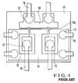
- a low-noise transistor having a pattern as shown in Fig. 4 is conventionally widely used as a low-noise amplifying element for microwaves in the C to Ku bands.
- This pattern has a gate finger 12a, gate electrode pads 12, a source electrode pad 14, and a drain electrode pad 13.
- the gate finger 12a is straightly arranged on a pellet 11.
- the gate electrode pads 12 are led out from portions midway along the gate finger 12a to one side.
- the source electrode pad 14 surrounds the gate electrode pads 12.
- the drain electrode pad 13 is arranged on the other side of the source electrode pad 14 through the gate finger 12a.
- This pattern is called the ⁇ type pattern. Bonding wires 16 are connected to the respective electrode pads 12, 13, and 14 through bonding balls 17.
- this pattern has, e.g., a gate electrode pad 22, four gate fingers 22a, an H-shaped source electrode pad 24 and a source electrode path 24b, a source finger 24a, a drain electrode pad 23, two drain fingers 23a, and aerial wirings 25.
- the gate electrode pad 22 is arranged on a pellet 21.
- the four gate fingers 22a are led out from the gate electrode pad 22 to be parallel to each other.
- the source electrode pad 24 and the source electrode path 24b are arranged to sandwich the gate electrode pad 22 and the gate fingers 22a.
- the source finger 24a is led out from the source electrode path 24b and is arranged in a region sandwiched between the two central gate fingers 22a.
- the drain electrode pad 23 is arranged on the other side of the gate electrode pad 22 through the source electrode path 24b.
- the two drain fingers 23a are arranged in the two remaining regions sandwiched between the gate fingers 22a.
- the aerial wirings 25 connect the drain fingers 23a to lie across the source electrode path 24b. This pattern is called the H type pattern. Bonding wires 26 are connected to the respective electrode pads 22, 23, and 24 through bonding balls 27.
- the gate electrode pads 12 are surrounded by the source electrode pad 14.
- both the gate electrode pad 22 and the drain electrode pad 23 are sandwiched by the source electrode pad 24. Therefore, the area of the gate electrode pads 12 or gate electrode pad 22 and the area of the drain electrode pad 23 are limited by the source electrode pads 14 and 24. More specifically, within the pellets 11 and 21 having a limited size, it is impossible to form the gate electrode pads 12 and 22 and the drain electrode pad 23 to have a large size, and a defect tends to be caused by misalignment in bonding.
- a semiconductor device comprising a square pellet having first and second diagonal lines, a gate electrode pad arranged on one of two corners located on the first diagonal line on the pellet, a drain electrode pad arranged on the other of the two corners located on the first diagonal line on the pellet, a pair of source electrode pads arranged on two corners located on the second diagonal line on the pellet, and a source electrode path for connecting the source electrode pads to each other.
- Fig. 1 shows the element pattern of a low-noise microwave transistor according to the first embodiment of the present invention.
- the element pattern of this embodiment has a gate electrode pad 102, a drain electrode pad 103, and two source electrode pads 104.
- the gate electrode pad 102 is arranged on one of four corners on a square pellet 101 to be located on one diagonal line.
- the drain electrode pad 103 is arranged on the other of the corners located on this diagonal line.
- the source electrode pads 104 are arranged on the two corners located on the remaining diagonal line on the pellet 101.
- gate electrode pad 102 Four comb-like gate fingers 102a are led out from the gate electrode pad 102 to the central portion of the pellet 101.
- Two drain fingers 103a led out from the drain electrode pad 103 are arranged on the two regions sandwiched by the two end portion-side gate fingers 102a.
- the two source electrode pads 104 are connected to each other through a source electrode path 104b arranged between the gate electrode pad 102 and the distal ends of the drain fingers 103a led out from the drain electrode pad 103.
- the source electrode path 104b extends above the gate fingers 102a to lie across them through aerial wirings 105.
- a source finger 104a led out from the source electrode path 104b is arranged in a region sandwiched by the two central gate fingers 102a.
- Bonding wires 106 are respectively bonded to the gate electrode pad 102 and the drain electrode pad 103 through bonding balls 107. Two bonding wires 106 are bonded to each of the two source electrode pads 104 through bonding balls 107, resulting in a total of four bonding wires 106. Many bonding wires 106 are bonded to the source electrode pads 104 in this manner in order to decrease the source ground impedance so as to cope with a high frequency.
- the electrode pads i.e., the bonding pads 102, 103, and 104 are arranged on the four corners of the pellet 101, the areas of the respective bonding pads 102, 103, and 104 can be maintained as large as possible on the pellet 101 having a limited size.
- the total area of the bonding pads 102, 103, and 104 can be 100 ⁇ m 2 .
- the areas of the bonding pads 102, 103, and 104 can be increased, the allowable range of misalignment in bonding is enlarged, and the defective bonding rate can be decreased.
- the defective bonding rate can be decreased from 0.5% down to 0.01% or less.
- the bonding index speed increases, misalignment in bonding increases.
- the bonding index speed can be increased than in the conventional case. Therefore, the productivity can be improved by about 10%.
- the source electrode path 104b is formed by the aerial wirings.
- the gate fingers 102a may be formed by the aerial wirings.
- cross wirings may be used in which upper wirings are formed over lower wirings through an insulating film.
- Fig. 2 shows the element pattern of a low-noise microwave transistor according to the second embodiment of the present invention.
- a gate electrode pad 102, a drain electrode pad 103, and source electrode pads 104 form a pattern arrangement similar to that of Fig. 1, and a detail description thereof will thus be omitted.
- Six comb-like gate fingers 102a are led out from the gate electrode pad 102 to the central portion of a pellet 101.
- Three drain fingers 103a led out from the drain electrode pad 103 are arranged on three regions sandwiched by the two central gate fingers 102a and the two side gate fingers 102a.
- the two source electrode pads 104 are connected to each other through a source electrode path 104b arranged between the drain electrode pad 103 and the distal ends of the gate fingers 102a led out from the gate electrode pad 102.
- the drain fingers 103a extend above the source electrode path 104b to lie across it through aerial wirings 105.
- the two source fingers 104a led out from the source electrode path 104b are arranged on the two remaining regions sandwiched by the gate fingers 102a.
- Two bonding wires 106 are bonded to each of the gate electrode pad 102 and the drain electrode pad 103 through bonding balls 107.
- Another two bonding wires 106 are bonded to each of the two source electrode pads 104 through bonding balls 107, resulting in a total of four bonding wires 106.
- the drain fingers 103a are formed by the aerial wirings.
- the source electrode path 104b may be formed by the aerial wirings.
- cross wirings may be used in which upper wirings are formed over lower wirings through an insulating film.
- Fig. 3 shows the element pattern of a low-noise microwave transistor according to the third embodiment of the present invention.
- the same reference numerals are used to denote the same or equivalent portions as in Fig. 1, and a detailed description thereof will be omitted.
- the gap of gate fingers 102a and the size of bonding wires 106 and bonding balls 107 are not changed but other portions are made small, so that the area of a pellet 101 is decreased to about half.
- the positions of two source electrode pads 104 are replaced with the positions of the gate electrode pad 102 and a drain electrode pad 103 in Fig. 3.
- the gate electrode pad 102 and the drain electrode pad 103 are respectively arranged on the two corners located on one diagonal line and the two source electrode pads 104 are respectively arranged on the two corners located on the other diagonal line.
- the gate electrode pad 102 and drain electrode pad 103 can have larger areas than in the conventional case with respect to the areas of the source electrode pads 104 having the same size.
- the pellet 101 which is smaller than the conventional pellet 101 suffices, and downsizing of the pellet 101 can be realized.
- the areas of the gate electrode pad and drain electrode pad can be made larger than in the conventional case by arranging the gate, source, and drain electrode pads on the four corners of the pellet.
- the allowable range of misalignment in bonding is increased accordingly, so that the defective bonding rate is decreased, and the productivity is improved.
- the size of the pellet can be made smaller than the conventional pellet.
Landscapes
- Junction Field-Effect Transistors (AREA)
- Wire Bonding (AREA)
Applications Claiming Priority (2)
| Application Number | Priority Date | Filing Date | Title |
|---|---|---|---|
| JP8174752A JP2778587B2 (ja) | 1996-07-04 | 1996-07-04 | 半導体装置 |
| JP174752/96 | 1996-07-04 |
Publications (2)
| Publication Number | Publication Date |
|---|---|
| EP0817264A2 true EP0817264A2 (de) | 1998-01-07 |
| EP0817264A3 EP0817264A3 (de) | 1998-12-09 |
Family
ID=15984071
Family Applications (1)
| Application Number | Title | Priority Date | Filing Date |
|---|---|---|---|
| EP97110462A Withdrawn EP0817264A3 (de) | 1996-07-04 | 1997-06-26 | Halbleiteranordnung |
Country Status (5)
| Country | Link |
|---|---|
| US (1) | US5856687A (de) |
| EP (1) | EP0817264A3 (de) |
| JP (1) | JP2778587B2 (de) |
| KR (1) | KR100255060B1 (de) |
| TW (1) | TW519708B (de) |
Families Citing this family (5)
| Publication number | Priority date | Publication date | Assignee | Title |
|---|---|---|---|---|
| JPH11195973A (ja) * | 1998-01-07 | 1999-07-21 | Oki Electric Ind Co Ltd | 半導体装置及びそれを用いた双方向光mosリレー |
| US6373143B1 (en) | 1998-09-24 | 2002-04-16 | International Business Machines Corporation | Integrated circuit having wirebond pads suitable for probing |
| JP2003007727A (ja) * | 2001-06-22 | 2003-01-10 | Sanyo Electric Co Ltd | 化合物半導体装置 |
| US6774416B2 (en) * | 2001-07-16 | 2004-08-10 | Nanowave, Inc | Small area cascode FET structure operating at mm-wave frequencies |
| US7994632B2 (en) * | 2006-01-10 | 2011-08-09 | International Rectifier Corporation | Interdigitated conductive lead frame or laminate lead frame for GaN die |
Family Cites Families (8)
| Publication number | Priority date | Publication date | Assignee | Title |
|---|---|---|---|---|
| JPS566476A (en) * | 1979-06-28 | 1981-01-23 | Nec Corp | Ultrahigh frequency field effect transistor |
| JPS637008A (ja) * | 1986-06-27 | 1988-01-12 | Fujitsu Ltd | 進行波型分布増幅器 |
| DE69010546T2 (de) * | 1989-04-17 | 1995-02-09 | Matsushita Electric Ind Co Ltd | Hochfrequenz-Halbleiteranordnung. |
| JP2822739B2 (ja) * | 1992-01-21 | 1998-11-11 | 日本電気株式会社 | 半導体装置 |
| JPH05315369A (ja) * | 1992-05-08 | 1993-11-26 | Sharp Corp | 高周波用半導体装置 |
| JP2576773B2 (ja) * | 1993-10-29 | 1997-01-29 | 日本電気株式会社 | マルチフィンガー型電界効果トランジスタ |
| DE4444808B4 (de) * | 1993-12-17 | 2005-12-15 | Denso Corp., Kariya | Halbleitervorrichtung |
| JPH08172104A (ja) * | 1994-12-20 | 1996-07-02 | Nec Corp | 半導体装置 |
-
1996
- 1996-07-04 JP JP8174752A patent/JP2778587B2/ja not_active Expired - Fee Related
-
1997
- 1997-06-24 TW TW086108833A patent/TW519708B/zh not_active IP Right Cessation
- 1997-06-26 EP EP97110462A patent/EP0817264A3/de not_active Withdrawn
- 1997-07-03 KR KR1019970030792A patent/KR100255060B1/ko not_active Expired - Fee Related
- 1997-07-07 US US08/889,052 patent/US5856687A/en not_active Expired - Lifetime
Also Published As
| Publication number | Publication date |
|---|---|
| KR100255060B1 (ko) | 2000-05-01 |
| EP0817264A3 (de) | 1998-12-09 |
| JP2778587B2 (ja) | 1998-07-23 |
| TW519708B (en) | 2003-02-01 |
| JPH1022320A (ja) | 1998-01-23 |
| US5856687A (en) | 1999-01-05 |
| KR980012158A (ko) | 1998-04-30 |
Similar Documents
| Publication | Publication Date | Title |
|---|---|---|
| US5373188A (en) | Packaged semiconductor device including multiple semiconductor chips and cross-over lead | |
| EP0154998B1 (de) | Stromversorgungsleiter-Struktur in einer integrierten Halbleiterschaltung | |
| KR100328906B1 (ko) | 리드프레임의리드온칩내부리드를결합하는방법및장치 | |
| US5497031A (en) | Semiconductor device having semiconductor chip with backside electrode | |
| US6605873B1 (en) | Integrated electronic device comprising a mechanical stress protection structure | |
| US5757082A (en) | Semiconductor chips, devices incorporating same and method of making same | |
| US5672909A (en) | Interdigitated wirebond programmable fixed voltage planes | |
| US20110012245A1 (en) | Semiconductor device | |
| US4551789A (en) | Multilayer ceramic substrates with several metallization planes | |
| JPS5984542A (ja) | 高周波半導体集積回路 | |
| US5801450A (en) | Variable pitch stagger die for optimal density | |
| US20170154849A1 (en) | Semiconductor device comprising power elements in juxtaposition order | |
| US6121690A (en) | Semiconductor device having two pluralities of electrode pads, pads of different pluralities having different widths and respective pads of different pluralities having an aligned transverse edge | |
| JP4025044B2 (ja) | 半導体集積回路装置 | |
| US5856687A (en) | Semiconductor device with connected source electrode pads at diagonal corners | |
| JPH04171734A (ja) | 半導体装置 | |
| US6054763A (en) | Semiconductor device | |
| US6191491B1 (en) | Semiconductor integrated circuit device | |
| KR950010046B1 (ko) | 경사 주변 회로를 가진 집적회로 장치 | |
| JP2724193B2 (ja) | 半導体装置 | |
| JPH04364051A (ja) | 半導体装置 | |
| JPH065849A (ja) | 半導体素子の構造 | |
| US6984882B2 (en) | Semiconductor device with reduced wiring paths between an array of semiconductor chip parts | |
| US6975020B2 (en) | Semiconductor integrated circuit having pads layout for increasing signal integrity and reducing chip size | |
| KR0169365B1 (ko) | 표시 패널 및 그 제조 방법 |
Legal Events
| Date | Code | Title | Description |
|---|---|---|---|
| PUAI | Public reference made under article 153(3) epc to a published international application that has entered the european phase |
Free format text: ORIGINAL CODE: 0009012 |
|
| AK | Designated contracting states |
Kind code of ref document: A2 Designated state(s): DE GB |
|
| PUAL | Search report despatched |
Free format text: ORIGINAL CODE: 0009013 |
|
| AK | Designated contracting states |
Kind code of ref document: A3 Designated state(s): AT BE CH DE DK ES FI FR GB GR IE IT LI LU MC NL PT SE |
|
| 17P | Request for examination filed |
Effective date: 19990301 |
|
| AKX | Designation fees paid |
Free format text: DE GB |
|
| 17Q | First examination report despatched |
Effective date: 20020815 |
|
| RAP1 | Party data changed (applicant data changed or rights of an application transferred) |
Owner name: NEC COMPOUND SEMICONDUCTOR DEVICES, LTD. |
|
| STAA | Information on the status of an ep patent application or granted ep patent |
Free format text: STATUS: THE APPLICATION IS DEEMED TO BE WITHDRAWN |
|
| 18D | Application deemed to be withdrawn |
Effective date: 20021228 |