EP0817992B1 - Verfahren und vorrichtung zur auswahl eines optimalen bustaktsignals in einem hoch skalierbaren rechnersystem - Google Patents
Verfahren und vorrichtung zur auswahl eines optimalen bustaktsignals in einem hoch skalierbaren rechnersystem Download PDFInfo
- Publication number
- EP0817992B1 EP0817992B1 EP96910678.0A EP96910678A EP0817992B1 EP 0817992 B1 EP0817992 B1 EP 0817992B1 EP 96910678 A EP96910678 A EP 96910678A EP 0817992 B1 EP0817992 B1 EP 0817992B1
- Authority
- EP
- European Patent Office
- Prior art keywords
- system bus
- circuitry
- frequency
- cpu
- clock
- Prior art date
- Legal status (The legal status is an assumption and is not a legal conclusion. Google has not performed a legal analysis and makes no representation as to the accuracy of the status listed.)
- Expired - Lifetime
Links
Images



Classifications
-
- G—PHYSICS
- G06—COMPUTING OR CALCULATING; COUNTING
- G06F—ELECTRIC DIGITAL DATA PROCESSING
- G06F1/00—Details not covered by groups G06F3/00 - G06F13/00 and G06F21/00
- G06F1/04—Generating or distributing clock signals or signals derived directly therefrom
- G06F1/08—Clock generators with changeable or programmable clock frequency
Definitions
- the present invention relates to the field of computer systems. More specifically, the present invention relates to scaling of central processing unit (CPU) and system bus clock frequencies of computer systems.
- CPU central processing unit
- Scalability of a system product line is often critical to its success. Superior scalability allows a system product line to have multiple models optimized for different performance design points over a wide performance spectrum to be cost effectively manufactured. Additionally, purchasers may start with the lower cost low end performance models, and grow their systems as their computing requirements increase.
- a well designed modern server system often would offer a choice for the number of CPUs to be employed. Many of these well designed server systems also would offer a choice or choices for the CPU clock frequency or frequencies.
- the system bus In order to accommodate the different potential CPU clock frequencies, the system bus would be designed to operate in one of a number of complementary clock frequencies. The selection of the CPU and system bus clock frequencies would be predetermined and set via jumpers.
- a server system would allow the employment of 1-4 CPUs having 1-2 clock frequencies to be selected from 3 clock frequencies (e.g. 100, 180, 200 MHz), and a system bus having a clock frequency to be selected from 3 other clock frequencies (e.g. 50, 60 and 66 MHz), with the ratio of any CPU clock frequency to system bus clock frequency to be one of 4 choices (2:1, 3:1, 4:1 and 5:1), the optimal selection will have to be made from almost 100 possible combinations.
- 3 clock frequencies e.g. 100, 180, 200 MHz
- 3 other clock frequencies e.g. 50, 60 and 66 MHz
- first exemplary computer system 10 comprises CPU boards 12a and 12b having CPUs 14a and 14b of a first type and CPUs 16a and 16b of a second type.
- CPUs 14a and 14b have a first maximum clock frequency
- CPUs 16a and 16b have a second maximum clock frequency.
- First exemplary computer system 10 also comprises system bus 18, cache memory 20, main memory 22 and memory controller 24 coupled to each other and to CPU boards 12a and 12b as shown.
- first exemplary computer system 10 further comprises oscillators 27, oscillator output selector 26 and complementary control circuitry, which is a bus clock frequency preference selector 28 under this embodiment.
- Oscillators 27, Oscillator output selector 26 and bus clock frequency preference selector 28 are disposed on the motherboard 30 of first exemplary computer system 10. Furthermore, under this embodiment, CPU boards 12a and 12b are to also include ratio and frequency code generators 30a and 30b.
- CPU boards 12a and 12b, CPUs 14a-14b and 16a-16b, system bus 18, cache memory 20, main memory 22 and memory controller 24 perform their conventional functions, which are well known, and the constitutions of these elements are also well known. Thus, these elements will not be otherwise further described.
- Oscillators 27 are used to output multiple series' of clock pulses having different clock frequencies, e.g. 66 MHz, 50 MHz, and so forth.
- Oscillator output selector 26 is used to select one of these series' of clock pulses whose clock frequency would be optimal for CPUs 14a-14b and 16a-16b.
- the clock pulses are provided to the oscillator output selector 26 at predetermined input terminals.
- the oscillator output selector 26 can rely on the fact that the clock pulses output by a 66 MHz oscillator are provided at a first input terminal, whereas the clock pulses output by a 50 MHz oscillator are provided at a second input terminal, and so forth.
- Oscillator output selector 26 makes its selection in accordance to control signal OSCSEL provided by control circuitry or bus clock frequency preference selector 28 under this embodiment.
- Control circuitry, or bus clock frequency preference selector 28 outputs OSCSEL to control the selection being made by oscillator output selector 26, in accordance to control inputs received.
- Bus clock frequency preference selector 28 receives encoded system bus clock frequency preferences from CPU boards 12a and 12b as control inputs, and in response, bus clock frequency preference selector 28 outputs OSCSEL in accordance to the lowest bus clock frequency preference denoted, thereby causing oscillator output selector 26 to select the series of clock pulses having a frequency that is equal to or slower than the slowest preferred frequency.
- the system bus clock frequency preferences are encoded and prestored in ratio and frequency code generators 30a and 30b of CPU boards 12a and 12b.
- the system bus clock frequency preference encodings are output by ratio and frequency code generators 30a and 30b at system reset.
- CPU clock frequency to system bus clock frequency ratios are also encoded and prestored in ratio and frequency code generators 30a and 30b of CPU boards 12a and 12b.
- the CPU clock frequency to system bus clock frequency ratio encodings are also output and provided to on board CPUs 14a-14b and 16a-16b by ratio and frequency code generators 30a and 30b at system reset.
- second exemplary computer system 100 comprises CPU boards 102a and 102b having CPUs 104a and 104b of a third type and CPUs 106a and 106b of a fourth type.
- CPUs 104a and 104b have a third maximum clock frequency
- CPUs 106a and 106b have a fourth maximum clock frequency.
- Second exemplary computer system 100 also comprises system bus 108, cache memory 110, main memory 112 and memory controller 114 coupled to each other and to CPU boards 102a and 120b as shown.
- second exemplary computer system 100 further comprises oscillators 117, oscillator output selector 116 and complementary control circuitry, which is a ratio and selection look-up circuit 118 under this embodiment.
- Oscillators 117, oscillator output selector 116 and ratio and selection look-up circuit 118 are disposed on motherboard 120 of exemplary computer system 100.
- CPU boards 102a and 102b are to also include CPU type output circuits 120a and 120b.
- CPU boards 102a and 102b, CPUs 104a-104b and 106a-106b, system bus 108, cache memory 110, main memory 112 and memory controller 114 perform their conventional functions, which are well known, and the constitutions of these elements are also well known. Thus, these elements will not be otherwise further described.
- oscillators 117 output multiple series of clock pulses having different clock frequencies, e.g. 66 MHz, 50 MHz, and so forth.
- Oscillator output selector 116 is used to select one of these series' of clock pulses whose clock frequency would be optimal for CPU 104a-104b and 106a-106b as well as for system bus 108.
- the clock pulses are provided to the oscillator output selector 116 at predetermined input terminals.
- the oscillator output selector 116 can rely on the fact that the clock pulses output by a 66 MHz oscillator are provided at a first input terminal, whereas the clock pulses output by a 50 MHz oscillator are provided at a second input terminal, and so forth.
- Oscillator output selector 116 makes its selection in accordance to control signal OSCSEL provided by ratio and selection look-up circuit 118 under this embodiment.
- Control circuitry, or ratio and selection look-up circuit 118 outputs OSCSEL to control the selection being made by oscillator output selector 116, and CPU clock frequency to system bus clock frequency ratios to on board CPUs 104a-104b and 106a-106b, in accordance to control inputs received.
- Ratio and selection look-up circuit 118 receives CPU types from CPU boards 102a-102b as control inputs.
- the CPU types correspond to CPU maximum operating frequency and base system bus operating frequency pairs.
- CPU type X corresponds to a CPU having a maximum operating frequency of 180 MHz and a base system bus operating frequency of 60 MHz.
- CPU types are prestored in CPU type output circuits 120a-120b of CPU boards 102a-102b, and output at system reset.
- Optimal system bus clock frequencies and optimal CPU clock frequency to system bus ratios for the various CPU clock frequency combinations are predetermined, encoded, and the encodings are prestored in ratio and selection lookup circuit 118.
- the optimal system bus clock frequency and the optimal CPU clock frequency to system bus clock frequency ratio are determined based on maximized total CPU clock frequency utilization.
- ratio and selection look-up circuit 118 causes oscillator output selector 116 to select the series of clock pulses having a clock frequency that will allow exemplary computer system 100 to maximize the total CPU clock frequencies utilized.
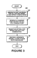
- the first step is to generate the CPU clock frequency utilizations for all CPU clock frequency and system bus clock frequency combinations presently supported and expected to be supported in the product life of the particular family of CPUs, step 132.
- they are generated in a matrix form.
- they are generated using multiple utilization matrices 140a-140c.
- utilization matrix 140a contains the CPU clock frequency utilizations for CPU clock frequencies 100 MHz, 150 MHZ etc.
- utilization matrix 104b when operated in conjunction with system bus clock frequencies of 50 MHz, 60 MHz, and 66 MHz, utilization matrix 104b contains the CPU clock frequency utilizations for CPU clock frequencies 120 MHz, 180 MHz, and so forth. More specifically, for a CPU clock frequency of 180 MHz, 150 MHz, 180 MHz, and 133 MHz of CPU clock frequencies will be utilized, depending on whether the system bus clock frequency is 50 MHz, 60 MHz or 66 MHz, since at most the CPU can operate at 3x, 3x, and 2x of the system bus frequency.
- a total CPU clock frequency utilization matrix covering all CPU clock frequency combinations is generated, step 134.
- each row of the total utilization matrix will contain the total CPU clock frequency utilizations 144 for a particular CPU clock frequency combination.
- the CPU clock frequency utilizations 142a for CPU clock frequency 200 MHz and the CPU dock frequency utilizations 142b for CPU clock frequency 180 MHz are combined to generate the total CPU clock frequency utilizations 144 for the CPU clock frequency combination of 200 MHz x 180 MHz.
- the total CPU clock frequency utilizations 144 would be 350 MHz, 360 MHz and 333 MHz respectively.
- an optimal system bus frequency is selected for each CPU clock frequency combination by selecting the maximum total CPU clock frequency utilization, step 136. For example, as shown in Figure 4 , upon comparing the total CPU clock frequency utilizations for CPU clock frequency combination of 200 x 180, 60 MHz would be selected as the optimal system bus frequency, since only a total of 360 MHz of CPU clock frequency would be utilized.
- the optimal system bus clock frequency and the corresponding CPU clock frequency to system bus clock frequency ratios are encoded, and the encodings are prestored into the ratio and selection lookup circuitry 118, step 138.
- a selection code for selecting the oscillator generating clock pulses having a frequency of 60 MHz, and codes denoting the CPU clock frequency to system bus dock frequency ratios to be 3:1 in both cases are prestored into the ratio and selection lookup circuitry 118.
- the above described maximized total CPU clock frequency utilization approach to determining the optimal system bus clock frequencies and CPU clock frequency to system bus clock frequency ratios for various CPU clock frequency combinations may be implemented in software, using any number of well known programming language, including but not limited to C, on any number of well known computer systems, including but not limited to Pentium® processor based computer systems. Pentium is a registered trademark of Intel Corporation.
Landscapes
- Engineering & Computer Science (AREA)
- Theoretical Computer Science (AREA)
- Physics & Mathematics (AREA)
- General Engineering & Computer Science (AREA)
- General Physics & Mathematics (AREA)
- Information Transfer Systems (AREA)
- Executing Machine-Instructions (AREA)
Claims (12)
- Vorrichtung, aufweisend:Zentraleinheiten (CPUs) (104a, 104b, 106a, 106b);einen Systembus (108);erste Schaltungen (118), die betriebsfähig sind, bei Systemrücksetzungszeit erste Steuereingaben auszugeben, welche die Art der CPUs anzeigen;zweite Schaltungen (116), die mit den ersten Schaltungen (118) gekoppelt und betriebsfähig sind, die ersten Steuereingaben zu empfangen, eine CPU-Taktfrequenzverwendungsmatrix zu generieren, die CPU-Taktfrequenzkombinationen für mehrere verfügbare Systembustakte für den Systembus (108) in Übereinstimmung mit den empfangenen ersten Steuereingaben abdeckt, und einen Systembustakt aus der Verwendungsmatrix auszuwählen, wobei der Systembustakt eine Taktfrequenz aufweist, die auf den Arten der CPUs (104a, 104b, 106a, 106b) basiert, wie definiert durch die empfangenen ersten Steuereingaben, und wobei der Systembus (108) mit den zweiten Schaltungen (116) gekoppelt ist.
- Vorrichtung nach Anspruch 1, wobei,
die ersten Schaltungen (118) bei Systemrücksetzungszeit erste Systembustaktfrequenz-Präferenzinformationen als die ersten Systembusauswahlsteuereingaben ausgeben; und
die zweiten Schaltungen (116) eine Serie von Taktsignalen als den Systembustakt auswählen, die eine Frequenz aufweisen, die gleich oder langsamer als die langsamste empfangene Systembustaktpräferenz ist. - Vorrichtung nach Anspruch 1, wobei,
die ersten Schaltungen (118) bei Systemrücksetzungszeit erste CPU-Taktfrequenzinformationen als die ersten Systembusauswahlsteuereingaben ausgeben; und
die zweiten Schaltungen (116) eine Serie von Taktsignalen auswählen, die eine Frequenz aufweisen, die dem System ermöglicht, die gesamte CPU-Frequenznutzung als den Systembustakt im Hinblick auf die ersten empfangenen Prozessortaktfrequenzinformationen zu maximieren. - Vorrichtung nach Anspruch 3, wobei die ersten Schaltungen (118) die ersten CPU-Taktfrequenzinformationen durch das Ausgeben erster Informationen über die CPU-Art, die direkt einer ersten CPU-Frequenz und einer ersten passenden Basissystembusfrequenz entspricht, implizit ausgeben.
- Vorrichtung nach Anspruch 1, wobei die zweiten Schaltungen (116) aufweisen:ein Oszillatorausgangswahlschalter, um eine von mehreren Serien von Taktsignalen auszuwählen, die unterschiedliche Frequenzen aufweisen, welche durch Oszillatoren des Systems als der Systembustakt ausgegeben werden; undSteuerschaltungen, die mit den ersten Schaltungen (118) und dem Oszillatorausgangswahlschalter gekoppelt sind, um die ersten Steuereingaben zu empfangen, welche durch die ersten Schaltungen (118) ausgegeben werden, und die Auswahl zu kontrollieren, die durch den Oszillatorausgangswahlschalter in Übereinstimmung mit den empfangenen ersten Steuereingaben getroffen wird.
- Vorrichtung nach Anspruch 5, wobei
die Steuerschaltungen erste Präferenzinformationen über die Systembusfrequenz von den ersten Schaltungen (118) als die ersten Steuereingaben empfangen; und
die Steuerschaltungen den Oszillatorausgangswahlschalter veranlassen, eine Serie von Taktsignalen auszuwählen, die eine Frequenz aufweisen, die gleich oder langsamer ist als die langsamste Präferenz, die von den ersten Schaltungen (118) empfangen wurde. - Vorrichtung nach Anspruch 5, wobei
die Steuerschaltungen erste Prozessorfrequenzinformationen von den ersten Schaltungen (118) als erste Steuereingaben empfangen; und
die Steuerschaltungen den Oszillatorausgangswahlschalter veranlassen, eine Serie von Taktsignalen auszuwählen, die eine Frequenz aufweisen, die dem System ermöglicht, die gesamte CPU-Frequenznutzung als den Systembustakt im Hinblick auf die ersten empfangenen CPU-Frequenzinformationen zu maximieren. - Vorrichtung nach Anspruch 7, wobei die Steuerschaltungen Schaltungselemente aufweisen, um Auswahlsteuersignale vorzuspeichern, die an den Oszillatorausgangswahlschalter für verschiedene CPU-Frequenzkombinationen auszugeben sind.
- Vorrichtung nach Anspruch 5, wobei die Steuerschaltungen ferner zur gleichen Zeit Verhältnisinformationen von CPU-Taktfrequenz zu Systembustaktfrequenz an die CPUs (104a, 104b, 106a, 106b) des Systems ausgeben.
- Vorrichtung nach Anspruch 9, wobei die Steuerschaltungen Schaltungselemente aufweisen, um Verhältnisinformationen von CPU-Taktfrequenz zu Systembustaktfrequenz vorzuspeichern, die an die CPUs (104a, 104b, 106a, 106b) des Systems für verschiedene CPU-Frequenzkombinationen auszugeben sind.
- Vorrichtung nach Anspruch 1, wobei die ersten Schaltungen (118) ferner zur gleichen Zeit Verhältnisinformationen von CPU-Taktfrequenz zu Systembustaktfrequenz an eine oder mehrere CPUs (104a, 104b, 106a, 106b) des Systems ausgeben.
- Vorrichtung nach Anspruch 1, wobei
die Vorrichtung ferner dritte Schaltungen aufweist, um bei Systemrücksetzungszeit zweite Steuereingaben auszugeben;
wobei die zweiten Schaltungen (116) ferner mit den dritten Schaltungen gekoppelt sind, um die zweiten Steuereingaben zu empfangen und den Systembustakt für den Systembus (108) auch in Übereinstimmung mit den empfangenen zweiten Steuereingaben auszuwählen, und der Systembustakt eine Taktfrequenz aufweist, die für CPUs (104a, 104b, 106a, 106b) von einem System optimal ist, wie definiert durch die empfangenen ersten sowie zweiten Steuereingaben.
Applications Claiming Priority (3)
| Application Number | Priority Date | Filing Date | Title |
|---|---|---|---|
| US414290 | 1982-09-03 | ||
| US41429095A | 1995-03-31 | 1995-03-31 | |
| PCT/US1996/004412 WO1996030819A1 (en) | 1995-03-31 | 1996-03-28 | Method and apparatus for selecting an optimal system bus clock in a highly scalable computer system |
Publications (3)
| Publication Number | Publication Date |
|---|---|
| EP0817992A1 EP0817992A1 (de) | 1998-01-14 |
| EP0817992A4 EP0817992A4 (de) | 2002-02-13 |
| EP0817992B1 true EP0817992B1 (de) | 2014-12-24 |
Family
ID=23640822
Family Applications (1)
| Application Number | Title | Priority Date | Filing Date |
|---|---|---|---|
| EP96910678.0A Expired - Lifetime EP0817992B1 (de) | 1995-03-31 | 1996-03-28 | Verfahren und vorrichtung zur auswahl eines optimalen bustaktsignals in einem hoch skalierbaren rechnersystem |
Country Status (5)
| Country | Link |
|---|---|
| US (1) | US6026231A (de) |
| EP (1) | EP0817992B1 (de) |
| KR (1) | KR100294003B1 (de) |
| AU (1) | AU5380796A (de) |
| WO (1) | WO1996030819A1 (de) |
Families Citing this family (11)
| Publication number | Priority date | Publication date | Assignee | Title |
|---|---|---|---|---|
| US6047373A (en) * | 1997-01-02 | 2000-04-04 | Intel Corporation | Method and apparatus for setting the operating parameters of a computer system |
| JP2002041452A (ja) * | 2000-07-27 | 2002-02-08 | Hitachi Ltd | マイクロプロセッサ、半導体モジュール及びデータ処理システム |
| KR100369463B1 (ko) * | 2000-12-21 | 2003-01-24 | 엘지전자 주식회사 | 휴대용 컴퓨터에서의 호스트 버스 클럭 가변 제어방법 |
| JP2002215599A (ja) * | 2001-01-18 | 2002-08-02 | Mitsubishi Electric Corp | マルチプロセッサシステムおよびその制御方法 |
| US7058824B2 (en) * | 2001-06-15 | 2006-06-06 | Microsoft Corporation | Method and system for using idle threads to adaptively throttle a computer |
| DE10240086A1 (de) * | 2002-08-30 | 2004-03-11 | Fujitsu Siemens Computers Gmbh | Verfahren und Anordnung zum Betreiben von peripheren Einheiten an einem BUS |
| US20050210310A1 (en) * | 2002-08-30 | 2005-09-22 | Fujitsu Siemens Computers Gmbh | Method and apparatus for operating peripheral units on a bus |
| US20050220942A1 (en) * | 2004-03-15 | 2005-10-06 | Hongyu Wu | Easy to peal vacuum packaging bags |
| TWI257553B (en) * | 2004-06-04 | 2006-07-01 | Asustek Comp Inc | Multiple over-clocking main board and control method thereof |
| US8245070B2 (en) * | 2008-12-30 | 2012-08-14 | Intel Corporation | Method for optimizing voltage-frequency setup in multi-core processor systems |
| US10761560B2 (en) | 2018-10-15 | 2020-09-01 | Huawei Technologies Co., Ltd. | Method and apparatus for transaction based propagated clock-gating for low power design |
Family Cites Families (6)
| Publication number | Priority date | Publication date | Assignee | Title |
|---|---|---|---|---|
| US5092280A (en) * | 1988-04-19 | 1992-03-03 | Westinghouse Electric Corp. | Pressure pulse cleaning apparatus |
| US5263172A (en) * | 1990-04-16 | 1993-11-16 | International Business Machines Corporation | Multiple speed synchronous bus having single clock path for providing first or second clock speed based upon speed indication signals |
| US5095280A (en) * | 1990-11-26 | 1992-03-10 | Integrated Circuit Systems, Inc. | Dual dot clock signal generator |
| GB2252432B (en) * | 1991-02-01 | 1994-09-28 | Intel Corp | Method and apparatus for operating a computer bus using selectable clock frequencies |
| US5448715A (en) * | 1992-07-29 | 1995-09-05 | Hewlett-Packard Company | Dual clock domain interface between CPU and memory bus |
| US5459855A (en) * | 1992-08-10 | 1995-10-17 | Hewlett-Packard Company | Frequency ratio detector for determining fixed frequency ratios in a computer system |
-
1996
- 1996-03-28 EP EP96910678.0A patent/EP0817992B1/de not_active Expired - Lifetime
- 1996-03-28 WO PCT/US1996/004412 patent/WO1996030819A1/en not_active Ceased
- 1996-03-28 AU AU53807/96A patent/AU5380796A/en not_active Abandoned
- 1996-03-28 KR KR1019970706058A patent/KR100294003B1/ko not_active Expired - Fee Related
-
1997
- 1997-12-24 US US08/998,147 patent/US6026231A/en not_active Expired - Lifetime
Also Published As
| Publication number | Publication date |
|---|---|
| KR100294003B1 (ko) | 2001-08-07 |
| EP0817992A1 (de) | 1998-01-14 |
| US6026231A (en) | 2000-02-15 |
| WO1996030819A1 (en) | 1996-10-03 |
| EP0817992A4 (de) | 2002-02-13 |
| KR19980702652A (ko) | 1998-08-05 |
| AU5380796A (en) | 1996-10-16 |
Similar Documents
| Publication | Publication Date | Title |
|---|---|---|
| EP0817992B1 (de) | Verfahren und vorrichtung zur auswahl eines optimalen bustaktsignals in einem hoch skalierbaren rechnersystem | |
| US5995016A (en) | Method and apparatus for N choose M device selection | |
| US5982195A (en) | Programmable logic device architectures | |
| EP0206083B1 (de) | Verfahren und Gerät zum Aneinanderpassen von Bussen verschiedener Breiten | |
| US5802393A (en) | Computer system for detecting and accessing BIOS ROM on local bus peripheral bus or expansion bus | |
| EP0453199B1 (de) | Rechnersystem mit synchronem Bus | |
| US5136180A (en) | Variable frequency clock for a computer system | |
| EP0015054A1 (de) | Verbindungssysteme mit Bus | |
| US7036009B2 (en) | Partition reconfiguration system, partition reconfiguration method, and partition reconfiguration program | |
| US5742188A (en) | Universal input data sampling circuit and method thereof | |
| KR100369092B1 (ko) | 데이타프로세서로부터어드레스신호와데이터신호를제공하는방법과데이터프로세서 | |
| EP0380092B1 (de) | Entscheidungsvorrichtung für Prioritätsfolge | |
| EP0229734A2 (de) | Mikroprogram-Steueranordnung | |
| US6147537A (en) | Reset circuit for flipflop | |
| US7032038B1 (en) | Configurable peripheral devices | |
| US6161188A (en) | Microprocessor having fuse control and selection of clock multiplier | |
| US5831556A (en) | Pin-reduced low power keyboard scanner | |
| US6192437B1 (en) | Transmission apparatus with control circuit/relay within each card providing connection to related card output depending on related slot ID/ redundancy/non-redundancy, working/protection signals | |
| JPH0728393A (ja) | 制御装置 | |
| US5940607A (en) | Device and method for automatically selecting a central processing unit driving frequency | |
| EP0100240A2 (de) | Verfahren und Vorrichtung zur Systemgenerierung | |
| US6121790A (en) | Programmable logic device with enhanced multiplexing capabilities in interconnect resources | |
| US4464772A (en) | Frequency synthesizer for providing a pseudo-constant frequency signal | |
| GB2126013A (en) | Microprocessor system | |
| KR0167646B1 (ko) | 중앙처리장치의 선택장치 |
Legal Events
| Date | Code | Title | Description |
|---|---|---|---|
| PUAI | Public reference made under article 153(3) epc to a published international application that has entered the european phase |
Free format text: ORIGINAL CODE: 0009012 |
|
| 17P | Request for examination filed |
Effective date: 19971024 |
|
| AK | Designated contracting states |
Kind code of ref document: A1 Designated state(s): DE FR GB IT |
|
| A4 | Supplementary search report drawn up and despatched |
Effective date: 20020102 |
|
| AK | Designated contracting states |
Kind code of ref document: A4 Designated state(s): DE FR GB IT |
|
| 17Q | First examination report despatched |
Effective date: 20070914 |
|
| GRAP | Despatch of communication of intention to grant a patent |
Free format text: ORIGINAL CODE: EPIDOSNIGR1 |
|
| INTG | Intention to grant announced |
Effective date: 20140704 |
|
| GRAS | Grant fee paid |
Free format text: ORIGINAL CODE: EPIDOSNIGR3 |
|
| GRAA | (expected) grant |
Free format text: ORIGINAL CODE: 0009210 |
|
| AK | Designated contracting states |
Kind code of ref document: B1 Designated state(s): DE FR GB IT |
|
| REG | Reference to a national code |
Ref country code: GB Ref legal event code: FG4D |
|
| REG | Reference to a national code |
Ref country code: DE Ref legal event code: R096 Ref document number: 69638679 Country of ref document: DE Effective date: 20150219 |
|
| REG | Reference to a national code |
Ref country code: FR Ref legal event code: PLFP Year of fee payment: 20 |
|
| PGFP | Annual fee paid to national office [announced via postgrant information from national office to epo] |
Ref country code: DE Payment date: 20150324 Year of fee payment: 20 |
|
| PGFP | Annual fee paid to national office [announced via postgrant information from national office to epo] |
Ref country code: GB Payment date: 20150325 Year of fee payment: 20 Ref country code: FR Payment date: 20150309 Year of fee payment: 20 |
|
| REG | Reference to a national code |
Ref country code: DE Ref legal event code: R097 Ref document number: 69638679 Country of ref document: DE |
|
| PLBE | No opposition filed within time limit |
Free format text: ORIGINAL CODE: 0009261 |
|
| STAA | Information on the status of an ep patent application or granted ep patent |
Free format text: STATUS: NO OPPOSITION FILED WITHIN TIME LIMIT |
|
| 26N | No opposition filed |
Effective date: 20150925 |
|
| PG25 | Lapsed in a contracting state [announced via postgrant information from national office to epo] |
Ref country code: IT Free format text: LAPSE BECAUSE OF FAILURE TO SUBMIT A TRANSLATION OF THE DESCRIPTION OR TO PAY THE FEE WITHIN THE PRESCRIBED TIME-LIMIT Effective date: 20141224 |
|
| REG | Reference to a national code |
Ref country code: DE Ref legal event code: R071 Ref document number: 69638679 Country of ref document: DE |
|
| REG | Reference to a national code |
Ref country code: GB Ref legal event code: PE20 Expiry date: 20160327 |
|
| PG25 | Lapsed in a contracting state [announced via postgrant information from national office to epo] |
Ref country code: GB Free format text: LAPSE BECAUSE OF EXPIRATION OF PROTECTION Effective date: 20160327 |