EP0818823A2 - Module à radio-fréquence et procédé de fabrication du module à radio-fréquence - Google Patents
Module à radio-fréquence et procédé de fabrication du module à radio-fréquence Download PDFInfo
- Publication number
- EP0818823A2 EP0818823A2 EP97109577A EP97109577A EP0818823A2 EP 0818823 A2 EP0818823 A2 EP 0818823A2 EP 97109577 A EP97109577 A EP 97109577A EP 97109577 A EP97109577 A EP 97109577A EP 0818823 A2 EP0818823 A2 EP 0818823A2
- Authority
- EP
- European Patent Office
- Prior art keywords
- metal film
- radio frequency
- frequency module
- semiconductor device
- module according
- Prior art date
- Legal status (The legal status is an assumption and is not a legal conclusion. Google has not performed a legal analysis and makes no representation as to the accuracy of the status listed.)
- Withdrawn
Links
Images


Classifications
-
- H—ELECTRICITY
- H10—SEMICONDUCTOR DEVICES; ELECTRIC SOLID-STATE DEVICES NOT OTHERWISE PROVIDED FOR
- H10W—GENERIC PACKAGES, INTERCONNECTIONS, CONNECTORS OR OTHER CONSTRUCTIONAL DETAILS OF DEVICES COVERED BY CLASS H10
- H10W44/00—Electrical arrangements for controlling or matching impedance
- H10W44/20—Electrical arrangements for controlling or matching impedance at high-frequency [HF] or radio frequency [RF]
-
- H—ELECTRICITY
- H10—SEMICONDUCTOR DEVICES; ELECTRIC SOLID-STATE DEVICES NOT OTHERWISE PROVIDED FOR
- H10W—GENERIC PACKAGES, INTERCONNECTIONS, CONNECTORS OR OTHER CONSTRUCTIONAL DETAILS OF DEVICES COVERED BY CLASS H10
- H10W70/00—Package substrates; Interposers; Redistribution layers [RDL]
- H10W70/60—Insulating or insulated package substrates; Interposers; Redistribution layers
- H10W70/67—Insulating or insulated package substrates; Interposers; Redistribution layers characterised by their insulating layers or insulating parts
- H10W70/68—Shapes or dispositions thereof
- H10W70/682—Shapes or dispositions thereof comprising holes having chips therein
-
- H—ELECTRICITY
- H10—SEMICONDUCTOR DEVICES; ELECTRIC SOLID-STATE DEVICES NOT OTHERWISE PROVIDED FOR
- H10W—GENERIC PACKAGES, INTERCONNECTIONS, CONNECTORS OR OTHER CONSTRUCTIONAL DETAILS OF DEVICES COVERED BY CLASS H10
- H10W70/00—Package substrates; Interposers; Redistribution layers [RDL]
- H10W70/60—Insulating or insulated package substrates; Interposers; Redistribution layers
- H10W70/67—Insulating or insulated package substrates; Interposers; Redistribution layers characterised by their insulating layers or insulating parts
- H10W70/68—Shapes or dispositions thereof
- H10W70/685—Shapes or dispositions thereof comprising multiple insulating layers
-
- H—ELECTRICITY
- H10—SEMICONDUCTOR DEVICES; ELECTRIC SOLID-STATE DEVICES NOT OTHERWISE PROVIDED FOR
- H10W—GENERIC PACKAGES, INTERCONNECTIONS, CONNECTORS OR OTHER CONSTRUCTIONAL DETAILS OF DEVICES COVERED BY CLASS H10
- H10W72/00—Interconnections or connectors in packages
- H10W72/071—Connecting or disconnecting
- H10W72/075—Connecting or disconnecting of bond wires
- H10W72/07541—Controlling the environment, e.g. atmosphere composition or temperature
- H10W72/07554—Controlling the environment, e.g. atmosphere composition or temperature changes in dispositions
-
- H—ELECTRICITY
- H10—SEMICONDUCTOR DEVICES; ELECTRIC SOLID-STATE DEVICES NOT OTHERWISE PROVIDED FOR
- H10W—GENERIC PACKAGES, INTERCONNECTIONS, CONNECTORS OR OTHER CONSTRUCTIONAL DETAILS OF DEVICES COVERED BY CLASS H10
- H10W72/00—Interconnections or connectors in packages
- H10W72/30—Die-attach connectors
- H10W72/381—Auxiliary members
-
- H—ELECTRICITY
- H10—SEMICONDUCTOR DEVICES; ELECTRIC SOLID-STATE DEVICES NOT OTHERWISE PROVIDED FOR
- H10W—GENERIC PACKAGES, INTERCONNECTIONS, CONNECTORS OR OTHER CONSTRUCTIONAL DETAILS OF DEVICES COVERED BY CLASS H10
- H10W72/00—Interconnections or connectors in packages
- H10W72/50—Bond wires
- H10W72/531—Shapes of wire connectors
- H10W72/536—Shapes of wire connectors the connected ends being ball-shaped
-
- H—ELECTRICITY
- H10—SEMICONDUCTOR DEVICES; ELECTRIC SOLID-STATE DEVICES NOT OTHERWISE PROVIDED FOR
- H10W—GENERIC PACKAGES, INTERCONNECTIONS, CONNECTORS OR OTHER CONSTRUCTIONAL DETAILS OF DEVICES COVERED BY CLASS H10
- H10W72/00—Interconnections or connectors in packages
- H10W72/50—Bond wires
- H10W72/541—Dispositions of bond wires
- H10W72/5445—Dispositions of bond wires being orthogonal to a side surface of the chip, e.g. parallel arrangements
-
- H—ELECTRICITY
- H10—SEMICONDUCTOR DEVICES; ELECTRIC SOLID-STATE DEVICES NOT OTHERWISE PROVIDED FOR
- H10W—GENERIC PACKAGES, INTERCONNECTIONS, CONNECTORS OR OTHER CONSTRUCTIONAL DETAILS OF DEVICES COVERED BY CLASS H10
- H10W72/00—Interconnections or connectors in packages
- H10W72/50—Bond wires
- H10W72/541—Dispositions of bond wires
- H10W72/547—Dispositions of multiple bond wires
-
- H—ELECTRICITY
- H10—SEMICONDUCTOR DEVICES; ELECTRIC SOLID-STATE DEVICES NOT OTHERWISE PROVIDED FOR
- H10W—GENERIC PACKAGES, INTERCONNECTIONS, CONNECTORS OR OTHER CONSTRUCTIONAL DETAILS OF DEVICES COVERED BY CLASS H10
- H10W72/00—Interconnections or connectors in packages
- H10W72/851—Dispositions of multiple connectors or interconnections
- H10W72/874—On different surfaces
- H10W72/884—Die-attach connectors and bond wires
-
- H—ELECTRICITY
- H10—SEMICONDUCTOR DEVICES; ELECTRIC SOLID-STATE DEVICES NOT OTHERWISE PROVIDED FOR
- H10W—GENERIC PACKAGES, INTERCONNECTIONS, CONNECTORS OR OTHER CONSTRUCTIONAL DETAILS OF DEVICES COVERED BY CLASS H10
- H10W72/00—Interconnections or connectors in packages
- H10W72/90—Bond pads, in general
- H10W72/951—Materials of bond pads
- H10W72/952—Materials of bond pads comprising metals or metalloids, e.g. PbSn, Ag or Cu
-
- H—ELECTRICITY
- H10—SEMICONDUCTOR DEVICES; ELECTRIC SOLID-STATE DEVICES NOT OTHERWISE PROVIDED FOR
- H10W—GENERIC PACKAGES, INTERCONNECTIONS, CONNECTORS OR OTHER CONSTRUCTIONAL DETAILS OF DEVICES COVERED BY CLASS H10
- H10W90/00—Package configurations
- H10W90/701—Package configurations characterised by the relative positions of pads or connectors relative to package parts
- H10W90/731—Package configurations characterised by the relative positions of pads or connectors relative to package parts of die-attach connectors
- H10W90/734—Package configurations characterised by the relative positions of pads or connectors relative to package parts of die-attach connectors between a chip and a stacked insulating package substrate, interposer or RDL
-
- H—ELECTRICITY
- H10—SEMICONDUCTOR DEVICES; ELECTRIC SOLID-STATE DEVICES NOT OTHERWISE PROVIDED FOR
- H10W—GENERIC PACKAGES, INTERCONNECTIONS, CONNECTORS OR OTHER CONSTRUCTIONAL DETAILS OF DEVICES COVERED BY CLASS H10
- H10W90/00—Package configurations
- H10W90/701—Package configurations characterised by the relative positions of pads or connectors relative to package parts
- H10W90/731—Package configurations characterised by the relative positions of pads or connectors relative to package parts of die-attach connectors
- H10W90/736—Package configurations characterised by the relative positions of pads or connectors relative to package parts of die-attach connectors between a chip and a stacked lead frame, conducting package substrate or heat sink
-
- H—ELECTRICITY
- H10—SEMICONDUCTOR DEVICES; ELECTRIC SOLID-STATE DEVICES NOT OTHERWISE PROVIDED FOR
- H10W—GENERIC PACKAGES, INTERCONNECTIONS, CONNECTORS OR OTHER CONSTRUCTIONAL DETAILS OF DEVICES COVERED BY CLASS H10
- H10W90/00—Package configurations
- H10W90/701—Package configurations characterised by the relative positions of pads or connectors relative to package parts
- H10W90/751—Package configurations characterised by the relative positions of pads or connectors relative to package parts of bond wires
- H10W90/754—Package configurations characterised by the relative positions of pads or connectors relative to package parts of bond wires between a chip and a stacked insulating package substrate, interposer or RDL
-
- H—ELECTRICITY
- H10—SEMICONDUCTOR DEVICES; ELECTRIC SOLID-STATE DEVICES NOT OTHERWISE PROVIDED FOR
- H10W—GENERIC PACKAGES, INTERCONNECTIONS, CONNECTORS OR OTHER CONSTRUCTIONAL DETAILS OF DEVICES COVERED BY CLASS H10
- H10W90/00—Package configurations
- H10W90/701—Package configurations characterised by the relative positions of pads or connectors relative to package parts
- H10W90/751—Package configurations characterised by the relative positions of pads or connectors relative to package parts of bond wires
- H10W90/756—Package configurations characterised by the relative positions of pads or connectors relative to package parts of bond wires between a chip and a stacked lead frame, conducting package substrate or heat sink
-
- Y—GENERAL TAGGING OF NEW TECHNOLOGICAL DEVELOPMENTS; GENERAL TAGGING OF CROSS-SECTIONAL TECHNOLOGIES SPANNING OVER SEVERAL SECTIONS OF THE IPC; TECHNICAL SUBJECTS COVERED BY FORMER USPC CROSS-REFERENCE ART COLLECTIONS [XRACs] AND DIGESTS
- Y10—TECHNICAL SUBJECTS COVERED BY FORMER USPC
- Y10T—TECHNICAL SUBJECTS COVERED BY FORMER US CLASSIFICATION
- Y10T29/00—Metal working
- Y10T29/49—Method of mechanical manufacture
- Y10T29/49002—Electrical device making
- Y10T29/49117—Conductor or circuit manufacturing
- Y10T29/49124—On flat or curved insulated base, e.g., printed circuit, etc.
- Y10T29/49126—Assembling bases
-
- Y—GENERAL TAGGING OF NEW TECHNOLOGICAL DEVELOPMENTS; GENERAL TAGGING OF CROSS-SECTIONAL TECHNOLOGIES SPANNING OVER SEVERAL SECTIONS OF THE IPC; TECHNICAL SUBJECTS COVERED BY FORMER USPC CROSS-REFERENCE ART COLLECTIONS [XRACs] AND DIGESTS
- Y10—TECHNICAL SUBJECTS COVERED BY FORMER USPC
- Y10T—TECHNICAL SUBJECTS COVERED BY FORMER US CLASSIFICATION
- Y10T29/00—Metal working
- Y10T29/49—Method of mechanical manufacture
- Y10T29/49002—Electrical device making
- Y10T29/49117—Conductor or circuit manufacturing
- Y10T29/49124—On flat or curved insulated base, e.g., printed circuit, etc.
- Y10T29/4913—Assembling to base an electrical component, e.g., capacitor, etc.
-
- Y—GENERAL TAGGING OF NEW TECHNOLOGICAL DEVELOPMENTS; GENERAL TAGGING OF CROSS-SECTIONAL TECHNOLOGIES SPANNING OVER SEVERAL SECTIONS OF THE IPC; TECHNICAL SUBJECTS COVERED BY FORMER USPC CROSS-REFERENCE ART COLLECTIONS [XRACs] AND DIGESTS
- Y10—TECHNICAL SUBJECTS COVERED BY FORMER USPC
- Y10T—TECHNICAL SUBJECTS COVERED BY FORMER US CLASSIFICATION
- Y10T29/00—Metal working
- Y10T29/49—Method of mechanical manufacture
- Y10T29/49002—Electrical device making
- Y10T29/49117—Conductor or circuit manufacturing
- Y10T29/49124—On flat or curved insulated base, e.g., printed circuit, etc.
- Y10T29/49155—Manufacturing circuit on or in base
- Y10T29/49165—Manufacturing circuit on or in base by forming conductive walled aperture in base
Definitions
- the present invention relates to a radio frequency module operating at a frequency of several hundred MHz or higher and a method for fabricating the same. More particularly, the present invention relates to a radio frequency module including active elements (such as transmission power transistors) mounted on a printed circuit board and a method for fabricating the same.
- active elements such as transmission power transistors
- a typical "radio frequency module” implements a compact radio frequency circuit by mounting principally various chip components at a high density on a printed circuit board of a small size.
- a radio frequency module includes various active elements such as transmission power transistors and various kinds of small-sized passive elements or chip components such as resistors, capacitors and inductors. Both the active elements and the passive elements are mounted on a printed circuit board on which transmission lines such as microstrip lines have been formed.
- a radio frequency module operates at a frequency of several hundred MHz or higher and is typically used as a transmission section for various kinds of mobile communication units such as transceivers, cellular phone units and the like.
- a radio frequency module used as a transmission section generally implements a two-stage or three-stage radio frequency power amplifier circuit including a plurality of field effect transistors (hereinafter, simply referred to as "FETs").
- FETs field effect transistors
- the impedance of a radio frequency module viewed from an external circuit at the terminal thereof for inputting/outputting a radio frequency signal therethrough is adjusted to be 50 ⁇ and a direct current bias circuit is incorporated therein.
- a prior art metal base substrate for a radio frequency module is described, for example, in Japanese Laid-Open Patent Publication No. 3-272189.
- the metal base substrate described in this patent publication includes an insulating film, and a metal plate and a sheet of conductive metal foil which are adhered to both surfaces of the insulating film.
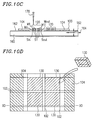
- FIG. 13 is a schematic cross-sectional view of the radio frequency module described in this patent publication.
- the radio frequency module shown in Figure 13 includes a circuit board 1310 and a semiconductor device 1320 which have been mounted on a radiator plate 1300 by means of soldering.
- the circuit board 1310 has a multi-layer structure of a metal film 1312 , a resin substrate 1314 and another metal film 1316 .
- a solder layer 1330 connects the circuit board 1310 and the semiconductor device 1320 to the radiator plate 1300 , respectively.
- the semiconductor device 1320 includes: an FET chip 1322 ; a package metal base 1323 ; a ceramic frame 1324 ; electrodes 1325 ; a source wire 1326 ; a gate wire 1327 ; a drain wire 1328 ; and lead terminals 1329 .
- the heat generated from the FET chip 1322 is passed through the package metal base 1323 and the solder layer 1330 to be transmitted into the radiator plate 1300 .
- the circuit board 1310 and the semiconductor device 1320 must be individually soldered to the radiator plate 1300 .
- the radio frequency module shown in Figure 13 has a problem in that the number of required process steps is increased. Also, the lead terminals 1329 must be connected to the circuit board 1310 of an individual module.
- the radio frequency module shown in Figure 13 cannot be tested until the radiator plate 1300 has been mounted. This is because the characteristics of the FET chip 1322 in an operation state are required to be tested under the same conditions as the conditions where the radio frequency module is actually used or the state where the radiator plate 1300 has already been mounted.
- the circuit board 1310 having a small area corresponding to an individual radio frequency module must be cut out from a circuit board having a larger area corresponding to a plurality of radio frequency modules. Consequently, a prior art radio frequency module cannot be tested before the circuit board 1310 for an individual radio frequency module is cut out from the larger sized circuit board.
- the radio frequency module can be tested only after the individual radio frequency module is completed. Therefore, in accordance with the conventional technologies, multiple radio frequency modules on an identical large-sized circuit board 1310 cannot be tested simultaneously.
- the conventional radio frequency module cannot reduce the number of necessary components and the number of necessary process steps, the reduction in size and cost of a single module and the automatic fabrication of the modules cannot be realized.
- the radio frequency module of the present invention includes an insulating substrate having a first metal film on a first principal surface thereof and a second metal film on a second principal surface thereof opposed to the first principal surface and a semiconductor device.
- the semiconductor device is thermally and electrically coupled to the second metal film, and a thickness of the second metal film is larger than that of the first metal film.
- the radio frequency module further includes an opening extending through the first metal film and the insulating substrate, and the semiconductor device is thermally and electrically coupled to the second metal film located inside the opening.
- the radio frequency module further includes a via hole for thermally and electrically coupling the first metal film to the second metal film, and the semiconductor device is thermally and electrically coupled to the second metal film through the via hole.
- the thickness of the first metal film is from about 10 ⁇ m to about 100 ⁇ m, both inclusive, and the thickness of the second metal film is from about 100 ⁇ m to about 1000 ⁇ m, both inclusive.
- the thickness of the first metal film is from about 30 ⁇ m to about 50 ⁇ m, both inclusive, and the thickness of the second metal film is from about 200 ⁇ m to about 300 ⁇ m, both inclusive.
- the first metal film or the second metal film includes a multi-layer structure of copper/nickel/gold layers or a multi-layer structure of copper/titanium/gold layers.
- the copper/nickel/gold layers and the copper/titanium/gold layers are stacked such that distances from a center in a thickness direction of the second metal film to the copper/nickel/gold layers and the copper/titanium/gold layers increase in this order.
- the semiconductor device is sealed inside a package.
- the semiconductor device is a bare chip.
- the semiconductor device is mounted on a metal block.
- the semiconductor device is coupled to the second metal film thermally at a heat resistance of about 3°C/W or less and electrically at an electrical resistance of about 1 ⁇ or less.
- the second metal film is patterned.
- At least a part of the patterned second metal film is electrically coupled to the first metal film through a via hole.
- a method for fabricating a radio frequency module includes the steps of providing an opening through an insulating substrate and a first metal film, the insulating substrate having the first metal film formed on a first principal surface thereof and a second metal film formed on a second principal surface thereof opposed to the first principal surface, a thickness of the second metal film being larger than that of the first metal film, and coupling thermally and electrically a semiconductor device to the second metal film located inside the opening.
- the method includes the steps of: thermally and electrically coupling the semiconductor device to the second metal film located inside the opening in an undivided substrate in which a plurality of said insulating substrates are combined; performing a test or an adjustment of characteristics of each of a plurality of radio frequency modules formed on the plurality of insulating substrates while the undivided substrate is still undivided and after the step of coupling; and dividing the undivided substrate into the plurality of insulating substrates after the step of performing the test or the adjustment.
- the method includes the steps of: thermally and electrically coupling the semiconductor device to the second metal film located inside the opening in an undivided substrate in which a plurality of said insulating substrates are combined; mounting shield members onto the plurality of insulating substrates while the undivided substrate is still undivided and after the step of coupling; and dividing the undivided substrate into the plurality of insulating substrates after the step of mounting the shield members.
- the step of thermally and electrically coupling the semiconductor device to the second metal film located inside the opening includes a step of mounting the semiconductor device onto the second metal film via solder.
- the step of providing the opening includes the steps of: opening a hole through the first metal film and the insulating substrate; selectively applying an adhesive onto any of the first metal film, the insulating substrate and the second metal film in accordance with a distance from an edge portion of the opened hole; and attaching the first metal film, the insulating substrate and the second metal film to each other.
- the step of providing the opening includes the steps of: attaching the first metal film, the insulating substrate and the second metal film to each other; and opening a hole through the first metal film and the insulating substrate after the step of attaching.
- a method for fabricating a radio frequency module includes the steps of providing a via hole through an insulating substrate having a first metal film formed on a first principal surface thereof and a second metal film formed on a second principal surface thereof opposed to the first principal surface, a thickness of the second metal film being larger than that of the first metal film, the via hole coupling thermally and electrically the first metal film to the second metal film, and thermally and electrically coupling a semiconductor device to the first metal film.
- the method includes the steps of: thermally and electrically coupling the semiconductor device to the first metal film in an undivided substrate in which a plurality of said insulating substrates are combined; performing a test or an adjustment of characteristics of each of a plurality of radio frequency modules formed on the plurality of insulating substrates while the undivided substrate is still undivided and after the step of coupling; and dividing the undivided substrate into the plurality of insulating substrates after the step of performing the test or the adjustment.
- the method includes the steps of: thermally and electrically coupling the semiconductor device to the first metal film in an undivided substrate in which a plurality of said insulating substrates are combined; mounting shield members onto the plurality of insulating substrates while the undivided substrate is still undivided and after the step of coupling; and dividing the undivided substrate into the plurality of insulating substrates after the step of mounting the shield members.
- the step of thermally and electrically coupling the semiconductor device to the first metal film includes a step of mounting the semiconductor device onto the first metal film via solder.
- the invention described herein makes possible the advantage of providing a radio frequency module and a method for fabricating the same which can reduce the number of required components and the number of required process steps for fabricating a smaller size individual module and is suitable for an automated operation test using machinery.
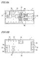
- Figure 1A is an enlarged plan view of the radio frequency module of the present invention as seen from above the principal surface thereof.
- Figure 1B is an enlarged cross-sectional view of the radio frequency module of the present invention.
- Figure 2A is an enlarged plan view of the radio frequency module of the present invention as seen from above the principal surface thereof.
- Figure 2B is an enlarged cross-sectional view of the radio frequency module of the present invention.
- Figure 3A is an enlarged plan view of the radio frequency module of the present invention as seen from above the principal surface thereof.
- Figure 3B is an enlarged cross-sectional view of the radio frequency module of the present invention.
- Figures 4A through 4D are views showing an exemplary set of steps of a method for fabricating the printed circuit board 1 shown in Figures 1A and 1B .
- Figures 5A through 5C are views showing another exemplary set of steps of a method for fabricating the printed circuit board 1 shown in Figures 1A and 1B .
- Figure 6A is a plan view of the radio frequency module of the present invention as seen from above the principal surface thereof.
- Figure 6B is a plan view of the radio frequency module of the present invention as seen from above the back surface thereof.
- Figure 6C is a cross-sectional view taken along the line VIC-VIC shown in Figure 6A .
- Figure 6D is a cross-sectional view taken along the line VID-VID shown in Figure 6A .
- Figure 7A is a plan view of the radio frequency module of the present invention as seen from above the principal surface thereof.
- Figure 7B is a cross-sectional view taken along the line VIIB-VIIB shown in Figure 7A .
- Figure 8A is a plan view of the radio frequency module of the present invention (on which a semiconductor device has not been mounted yet) as seen from above the principal surface thereof.
- Figure 8B is a plan view of the radio frequency module of the present invention as seen from above the back surface thereof.
- Figure 8C is a plan view of the radio frequency module of the present invention (on which the semiconductor device has already been mounted) as seen from above the principal surface thereof.
- Figure 8D is a cross-sectional view taken along the line VIIID-VIIID shown in Figure 8C .
- Figure 9A is a plan view of the semiconductor device 400 to be mounted onto the printed circuit board 1 shown in Figures 8A and 8B as seen from above a side opposite to a side including a ground electrode on the back surface of a package.
- Figure 9B is a plan view of the semiconductor device 400 to be mounted onto the printed circuit board 1 shown in Figures 8A and 8B as seen from above the side including the ground electrode on the back surface of the package.
- Figures 10A through 10F are views showing the process steps of a method for fabricating the radio frequency module of the present invention.
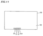
- Figure 11 is a plan view of a tester substrate 160 as seen from above a surface on which an undivided circuit board 100 is placed.
- Figure 12A is a view showing another exemplary substrate used for testing the radio frequency module.
- Figure 12B is a cross-sectional view illustrating the testing of the radio frequency module.
- Figure 13 is a schematic cross-sectional view showing a conventional radio frequency module.
- the radio frequency module of the present invention is typically used at a frequency of several hundred MHz or higher and preferably within the 800 MHz band.
- the radio frequency module to be described below implements a two-stage radio frequency amplifier circuit using two FETs.
- the circuit and the circuit configuration to which the present invention is applicable are not limited thereto. It should however be noted that the radio frequency module of the present invention can attain more remarkable effects when the radio frequency module is implemented as a circuit including a heat generating element.
- the radio frequency module of the present invention includes a printed circuit board and various elements mounted thereon.
- a circuit pattern for connecting respective components is provided for the printed circuit board.
- the printed circuit board has a "principal-surface metal film” on which the respective components are mounted and a "back-surface metal film", almost all the area of which is occupied by a ground pattern, to which a ground potential is applied.
- the principal-surface metal film and the back-surface metal film are typically metal films mainly made of copper (i.e., so-called “copper foil") and are attached onto both surfaces of an insulating substrate.
- the thickness of the back-surface metal film is larger than that of the principal-surface metal film.
- the thermal and electrical coupling between the heat generating components and the back-surface metal film is realized, for example, in any of the following manners:
- Figure 1A is an enlarged plan view of the radio frequency module of the present invention as seen from above the principal surface thereof.
- Figure 1B is an enlarged cross-sectional view of the radio frequency module of the present invention.
- the radio frequency module of the present invention includes a printed circuit board 1 .
- the printed circuit board 1 includes: an insulating substrate 30 ; a metal film 10 formed on the principal surface of the insulating substrate 30 ; and a metal film 20 formed on the back surface facing the principal surface.
- the thickness of the metal film 20 is larger than that of the metal film 10 .
- the metal films 10 and 20 are typically made of copper but may be made of any other metal material so long as the metal material has a sufficiently low electrical resistance.
- the insulating substrate 30 is typically made of a glass epoxy resin. However, the material usable for the insulating substrate 30 is not limited thereto but includes teflon and other resins such as a paper-based epoxy resin.
- the printed circuit board 1 has an opening 50 provided through the metal film 10 and the insulating substrate 30 . As shown in Figure 1A , a part of the upper surface of the metal film 20 is exposed inside the opening 50 and a semiconductor chip 40 is mounted on the exposed part of the surface of the metal film 20 .
- the semiconductor chip 40 is mounted in a bare chip manner, i.e., in a state where the semiconductor chip 40 has not been sealed inside a package yet.
- the bare chip mounting technique can reduce the thickness of the radio frequency module.
- the semiconductor chip 40 is die bonded onto the surface of the metal film 20 inside the opening 50 by means of soldering.
- the semiconductor chip 40 is thermally and electrically coupled to the metal film 20 by a solder layer 42 .
- a ground potential or the like can be applied to a predetermined terminal of the semiconductor chip 40 and the heat generated by the semiconductor chip 40 can be dissipated into the metal film 20 .
- the semiconductor chip 40 is coupled to the metal film 20 thermally at a heat resistance of about 3°C/W or less, and electrically at an electrical resistance of about 1 ⁇ or less.
- the thickness of the metal film 10 is preferably about 10 ⁇ m or more in order to prevent the inductance from being increased owing to the skin effects, and preferably less than about 100 ⁇ m in order to form a fine pattern suitable for a radio frequency circuit thereon. More preferably, the thickness of the metal film 10 is in an approximate range from about 30 ⁇ m to about 50 ⁇ m, both inclusive.
- the thickness of the metal film 20 is preferably about 100 ⁇ m or more.
- the thickness of the metal film 20 is preferably 1000 ⁇ m or less. More preferably, the thickness of the metal film 20 is in an approximate range from about 200 ⁇ m to about 300 ⁇ m, both inclusive.
- the drain, gate and source of the semiconductor chip 40 are wire bonded to a predetermined circuit pattern and the like via drain wires 44 , a gate wire 45 and source wires 46 .
- the wire bonding is performed by a generally used wire bonder.
- the radio frequency module of the present invention shown in Figures 1A and 1B includes the metal film 20 , having a thickness large enough to dissipate the heat generated from the semiconductor chip 40 , on the back surface of the printed circuit board 1 . As a result, since a radiator plate is no longer necessary, the number of required components and the size can be reduced.
- resin may be filled into the opening 50 so as to cover the semiconductor chip 40 in a bare chip state therewith.
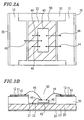
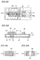
- FIG 2A is an enlarged plan view of the radio frequency module of the present invention as seen from above the principal surface thereof.
- Figure 2B is an enlarged cross-sectional view of the radio frequency module of the present invention.
- the radio frequency module shown in Figures 2A and 2B is different from the radio frequency module shown in Figures 1A and 1B in that the former radio frequency module includes a pair of stacked metal films 11 and 12 on the upper surface of the metal film 10 , a pair of stacked metal films 21 and 22 on the exposed upper surface of the metal film 20 and a pair of stacked metal films 23 and 24 on the lower surface of the metal film 20 .
- the metal films 11 , 21 and 23 are nickel or titanium, and the metal films 12 , 22 and 24 are gold. By forming these stacked metal films on the metal films 10 and 20 , the bonding using the drain wires 44 , the gate wire 45 and the source wires 46 can be performed more easily.
- Figure 3A is an enlarged plan view of the radio frequency module of the present invention as seen from above the principal surface thereof.
- Figure 3B is an enlarged cross-sectional view of the radio frequency module of the present invention.
- the radio frequency module shown in Figures 3A and 3B is different from the radio frequency module shown in Figures 1A and 1B in that the semiconductor chip 40 of the former radio frequency module is die bonded to a metal block 41 by means of soldering, and the metal block 41 is die bonded to the metal film 20 by means of soldering.
- the semiconductor chip 40 is preferably coupled to the metal film 20 thermally at a heat resistance of about 3°C/W or less, and electrically at an electrical resistance of about 1 ⁇ or less.
- a single semiconductor chip 40 is mounted on the metal block 41 .
- a plurality of semiconductor chips 40 may be mounted thereon. In such a case, first, a plurality of semiconductor chips 40 are mounted on the metal block 41 . Thereafter, the metal block 41 is mounted on the metal film 20 , thereby improving the mounting efficiency.
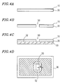
- Figures 4A through 4D are views showing an exemplary set of steps of a method for fabricating the printed circuit board 1 shown in Figures 1A and 1B .
- a metal film 10 and an insulating substrate 30 are attached to each other via an adhesive.
- an opening 50 is formed by punching the metal film 10 and the insulating substrate 30 which have been attached to each other.
- a metal film 20 is attached via an adhesive to the insulating substrate 30 through which the opening 50 has been formed, and a via hole 32 (to be described below) is formed for electrically coupling the metal film 10 to the metal film 20 .
- Figure 4D is a plan view of the lower surface of the insulating substrate 30 showing the range within which the adhesive is applied thereto as seen from the metal film 20 .
- the adhesive to be applied between the insulating substrate 30 and the metal film 20 shown in Figure 4C for attaching them to each other is preferably applied at the hatched portion shown in Figure 4D .
- the distance d is preferably in the range from about 2 mm to about 3 mm, both inclusive.
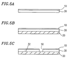
- Figures 5A through 5C are cross-sectional views showing another exemplary set of steps of a method for fabricating the printed circuit board 1 shown in Figures 1A and 1B .
- a metal film 10 and an insulating substrate 30 are attached to each other with an adhesive.
- a metal film 20 and the insulating substrate 30 are attached to each other with an adhesive.
- a portion of the attached metal film 10 and insulating substrate 30 is cut out to such a depth as to expose the upper surface of the metal film 20 , thereby forming an opening 50 . Then, a via hole 32 for electrically coupling these metal films 10 and 20 is formed.
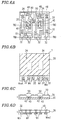
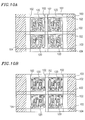
- Figure 6A is a plan view of the radio frequency module of the present invention as seen from above the principal surface thereof.
- Figure 6B is a plan view of the radio frequency module of the present invention as seen from above the back surface thereof.
- Figure 6C is a cross-sectional view taken along a line VIC-VIC shown in Figure 6A .
- Figure 6D is a cross-sectional view taken along a line VID-VID shown in Figure 6A .
- a metal film 10 patterned by etching for forming a radio frequency circuit is provided on the principal surface of the printed circuit board 1 .
- the thickness of the metal film 10 is about 40 ⁇ m, for example.
- Various chip components 48 such as resistors and capacitors are mounted onto the metal film 10 by means of soldering.
- Semiconductor chips 40 are die bonded by means of soldering onto the surface of metal film 20 which has been exposed inside the openings 50 .
- the terminals of the semiconductor chips 40 are electrically connected to the metal film 10 or the pattern on the principal surface by means of wire bonding.
- the semiconductor chips 40 are, for example, an anterior-stage FET and a posterior-stage FET forming a two-stage amplifier circuit.
- the circuit configuration, the type of the elements and the number of the elements are not limited to those exemplified in Figure 6A . Nevertheless, it should be noted that the present invention is particularly effective when the semiconductor chips 40 generate heat.
- a part of the nodes of the radio frequency circuit i.e., a part of the pattern of the metal film 10 , is electrically connected to the metal film 20 through the via holes 34 filled with metal. As a result, a ground potential is applied to the nodes.
- a metal film 20 on which a ground pattern is formed is provided so as to occupy a large area on the back surface of the printed circuit board 1 .
- patterns Min , M1 and Mout used for connecting the radio frequency module to external circuits are formed.
- the patterns Min , M1 and Mout for connection with external circuits (hereinafter, such patterns will be referred to as "external connection patterns") are used for connecting the radio frequency module to the mother circuit board of a mobile communication unit, for example.
- the via holes 32 are used for connecting the external connection patterns Min , M1 and Mout to the pattern of the metal film 10 on the principal surface.
- the external connection pattern Min receives a radio frequency signal and the external connection pattern Mout outputs a radio frequency signal amplified by the radio frequency module.
- the external connection patterns M1 receive a direct current bias voltage to be supplied to the gates and the drains thereof and then supply the voltage to the semiconductor chips 40 .
- the types, the number and the positions of the external connection patterns Min , M1 and Mout on the back surface of the printed circuit board 1 are not limited to those illustrated in Figure 6B but may be modified in accordance with the type of an external circuit to which the radio frequency module is connected.
- an effect can be attained in that it is no longer necessary to separately provide lead terminals.
- the metal film 20 has a sufficiently large thickness, another effect can also be attained in that a stable electrical connection with an external circuit can be maintained. Since the lead terminals are no longer necessary, the area which has conventionally been reserved for mounting the lead terminals in prior art radio frequency modules can be omitted and a step for mounting the lead terminals can be omitted during the fabrication thereof.
- the radio frequency module of the present invention a radiator plate and lead terminals which have been indispensable for conventional radio frequency modules are no longer necessary.
- the number of required components can be considerably reduced and the space reserved on the printed circuit board for mounting the radiator plate and the lead terminals can be eliminated. Consequently, the radio frequency module can be downsized and the number of fabrication process steps thereof can be reduced.
- a semiconductor device in a bare chip state can be directly die bonded onto the bottom of the opening of the printed circuit board, both the area and the thickness of the radio frequency module can be reduced.
- Figure 7A is a plan view of the radio frequency module of the present invention as seen from above the principal surface thereof.
- Figure 7B is a cross-sectional view taken along the line VIIB-VIIB shown in Figure 7A .
- the radio frequency module of the present invention shown in Figures 7A and 7B is different from the radio frequency module shown in Figures 6A to 6D in that the semiconductor chips 40 of the former radio frequency module are not mounted onto the printed circuit board 1 in a bare chip state, but after each of the semiconductor chips 40 has been sealed inside a package.
- a semiconductor device 400 includes a semiconductor chip 40 therein.
- the semiconductor chip 40 is directly die bonded onto a package metal base 402 .
- a ceramic frame 404 is formed on the package metal base 402 .
- Electrodes 406 are formed on the ceramic frame 404 and package lead terminals 408 are provided so as to be electrically connected to the electrodes 406 .
- the terminals of the semiconductor chip 40 are electrically connected to the electrodes 406 by means of wire bonding.
- the semiconductor device 400 is sealed with a resin such that the internal circuit components can be protected.
- the radio frequency module of the present invention is applicable not only to a semiconductor device in a bare chip state but also to a semiconductor device sealed inside a package. In the latter case, the same effects as those described above can also be attained.
- a semiconductor device is mounted on a principal-surface metal film.
- the principal-surface metal film is thermally and electrically coupled to a back-surface metal film through via holes.
- the semiconductor devices can be thermally and electrically coupled to the back-surface metal film without providing the openings of the first example through the printed circuit board.
- Figure 8A is a plan view of the radio frequency module of the present invention (on which a semiconductor device has not been mounted yet) as seen from above the principal surface thereof.
- Figure 8B is a plan view of the radio frequency module of the present invention as seen from above the back surface thereof.
- Figure 8C is a plan view of the radio frequency module of the present invention (on which the semiconductor device has already been mounted) as seen from above the principal surface thereof.
- Figure 8D is a cross-sectional view taken along a line VIIID-VIIID shown in Figure 8C .
- the printed circuit board 1 of the second example is not provided with openings 50 of the first example but with via holes 38 .
- the metal films 10 and 20 and the insulating substrate 30 of the printed circuit board 1 of the second example have the same thicknesses and are made of the same materials as those of the printed circuit board 1 of the first example.
- Figure 9A is a plan view of the semiconductor device 400 to be mounted onto the printed circuit board 1 shown in Figures 8A and 8B as seen from a side opposite to a side including a ground electrode on the back surface of a package.
- Figure 9B is a plan view of the semiconductor device 400 to be mounted onto the printed circuit board 1 shown in Figures 8A and 8B as seen from the side including the ground electrode on the back surface of the package.
- the semiconductor device 400 preferably has a ground electrode 412 on the back surface of the package, as shown in Figure 9B .
- the semiconductor device 400 further includes connection pins 414 to be connected to the metal film 10 or the pattern on the principal surface of the printed circuit board 1 .
- the via holes 38 shown in Figures 8A , 8B and 8D thermally and electrically couple the principal-surface metal film 10 to the back-surface metal film 20 .
- the number of the via holes 38 is not limited to three but may be increased or decreased in order to obtain a desired heat resistance and a desired electrical resistance.
- a semiconductor chip 40 has been molded and then sealed with a resin inside the package thereof.
- the semiconductor chip 40 is connected thermally and electrically to the ground electrode 412 inside the package, thereby dissipating the heat generated from the semiconductor chip 40 to the outside via the ground electrode 412 .
- the ground electrode 412 has been exposed on the back surface of the package such that the ground electrode 412 can be soldered with the principal-surface metal film 10 when the semiconductor device 400 is mounted onto the printed circuit board 1 .
- the semiconductor device 400 is disposed on the printed circuit board 1 such that the ground electrode 412 can be soldered with the metal film 10 in the vicinity of the via holes 38 . As a result, the heat generated from the semiconductor chip 40 inside the semiconductor device 400 is dissipated into the metal film 20 via the ground electrode 412 , the metal film 10 and the via holes 38 .
- the semiconductor device 400 is preferably disposed such that the via holes 38 are included within a region of the metal film 10 which faces the ground electrode 412 . More preferably, the semiconductor device 400 is disposed such that the via holes 38 are located just under the ground electrode 412 .
- the semiconductor chip 40 is thermally and electrically coupled to the metal film 20 via the ground electrode 412 , a solder layer (not shown), the metal film 10 and the via holes 38 .
- a ground potential for example, can be applied to the predetermined terminals of the semiconductor chip 40 and the heat generated from the semiconductor chip 40 can be dissipated into the metal film 20 .
- the semiconductor chip 40 is coupled to the metal film 20 thermally at a heat resistance of about 3°C/W or less, and electrically at an electrical resistance of about 1 ⁇ or less.
- the thickness of the metal film 20 is larger than that of the metal film 10 .
- the thickness of the metal film 10 is preferably about 10 ⁇ m or more in order to prevent the inductance from being increased owing to the skin effects and preferably less than about 100 ⁇ m in order to form a fine pattern suitable for a radio frequency circuit thereon. More preferably, the thickness of the metal film 10 is in an approximate range from about 30 ⁇ m to about 50 ⁇ m, both inclusive.
- the thickness of the metal film 20 is preferably about 100 ⁇ m or more.
- the thickness of the metal film 20 is preferably 1000 ⁇ m or less. More preferably, the thickness of the metal film 20 is in an approximate range from about 200 ⁇ m to about 300 ⁇ m, both inclusive.
- the external connection patterns 36 are electrically connected to the metal film 10 or the pattern on the principal surface through the via holes 32 .
- the external connection patterns 36 have the same functions as those of the external connection patterns Min , M1 and Mout of the first example.
- the external connection patterns 36 can be provided by patterning the metal film 20 in the second example. As a result, there is no need of providing the lead terminals.
- Figures 8C and 8D show a state where the semiconductor device 400 has been mounted on the printed circuit board 1 .
- the semiconductor device 400 shown in Figures 8C and 8D includes an integrated circuit (IC) chip therein, a separate semiconductor device such as an FET may also be provided instead.
- IC integrated circuit
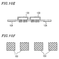
- FIGS 10A through 10F are views showing the process steps for fabricating the radio frequency module of the present invention.
- an undivided circuit board 100 for mounting a plurality of radio frequency modules thereon is fabricated.
- a plurality of circuit board divisions 120 are provided on the undivided circuit board 100 .
- Various components of a single radio frequency module are mounted in each circuit board division 120 .
- Each circuit board division 120 corresponds to the printed circuit board 1 shown in Figures 6A to 6D , for example.
- Division grooves 102 are formed on the surface of the undivided circuit board 100 in order to facilitate the division of the undivided circuit board 100 into the circuit board divisions 120 after the works performed on the radio frequency modules on the undivided circuit board 100 have been completed.
- the depth of the division grooves 102 is preferably about one-half of the thickness of the undivided circuit board 100 . In such a case, the division can be performed manually instead of using a machine.
- circuit board divisions 120 are provided on the undivided circuit board 100 .
- the number of the circuit board divisions 120 is not limited thereto.
- the respective steps including mounting various components, test and adjustment of the radio frequency modules and mounting of shield members can be performed more efficiently.
- ground electrodes 104 having sufficiently large areas are laid out around the plurality of circuit board divisions 120 , thereby stabilizing the ground potential. As a result, when the characteristics of the radio frequency modules are tested (to be described later), the test can be performed more stably.
- the components of the radio frequency modules are mounted into the respective circuit board divisions 120 .
- the semiconductor chip 40 and the chip components 48 shown in Figure 6A are mounted in each circuit board division 120 .
- the wire bonding for electrically connecting the semiconductor chip 40 shown in Figure 6A to the metal film 10 is also performed. That is to say, after the mounting step shown in Figure 10B and the connection of the radio frequency modules to external circuits (including testing equipment) are completed, the respective radio frequency modules are in an operable state.
- the respective radio frequency modules can be operated on the undivided circuit board 100 .
- the below-described works such as test and adjustment of the respective radio frequency modules and mounting of shield members can be performed before the undivided circuit board 100 is divided into the circuit board divisions 120 .
- the undivided circuit board 100 is fixed on a tester substrate 160 , thereby testing and/or adjusting the radio frequency modules. Almost the entire region of the upper surface of the tester substrate 160 is occupied by a ground electrode 162 , thereby stabilizing the ground potential and connecting the terminals of the circuit board divisions 120 corresponding to currently non-tested radio frequency modules to the ground.
- the radio frequency power input/output characteristics, the gain, the power efficiency and the like of the radio frequency module can be measured.
- a radio frequency input power is supplied through a pattern Sin
- a power amplified by the radio frequency module is output through a pattern Sout and a direct current bias is applied through patterns S1 to the radio frequency module.
- the respective patterns Sin , S1 and Sout are contacted with the associated terminals of the radio frequency module.
- FIG 11 is a plan view of the tester substrate 160 as seen from above the surface on which the undivided circuit board 100 is placed.
- the tester substrate 160 has patterns Sin , S1 and Sout (e.g., associated with the external connection patterns Min , M1 and Mout shown in Figure 6B , respectively) such that the radio frequency modules can be individually tested one by one.
- the pattern Sin receives a radio frequency signal output from the radio frequency module and the pattern Sout outputs a radio frequency signal to the radio frequency module.
- the patterns S1 supply a direct current bias to the radio frequency module. By applying a pressure thereto, the patterns Sin , S1 and Sout can be respectively connected to the external connection patterns Min , M1 and Mout of the radio frequency module at an electrical resistance sufficiently low for testing.
- a laser beam 170 is used, thereby varying the values of chip components 48 such as resistors and capacitors which are mounted on the radio frequency module and can be trimmed by laser. Then, the characteristics of the radio frequency module can be tested again after the characteristics of the radio frequency module have been adjusted.
- the location of the laser beam 170 may be fixed and the tester substrate 160 may be moved (as indicated by the arrows 164 ), for example.
- the tester substrate 160 may be moved (as indicated by the arrows 164 ), for example.
- a test and adjustment loop may be repeatedly performed a desired number of times by using machinery.
- the shield members 130 are mounted so as to cover the radio frequency modules in the respective circuit board divisions 120 therewith.
- the mounting of the shield members 130 shown in Figure 10D is performed after the test and the adjustment shown in Figure 10C have been completed.
- Each of the shield members 130 is made of a metallic thin plate, for example, and shields a completed radio frequency module from an electromagnetic interruption from an external circuit (e.g., a mobile communication unit) when the radio frequency module operates.
- the shield member 130 is soldered with the metal film 10 shown in Figure 6A and is electrically connected to the ground surface on the back surface of the printed circuit board through the via holes.
- Figure 10E is a cross-sectional view taken along the line XD-XD shown in Figure 10D .
- the test may be performed after the shield members 130 have been mounted as shown in Figure 10E .
- the radio frequency module incorporated into an actually used machine is actually operated, the radio frequency module is shielded by the shield member 130 .
- the radio frequency module can be tested more precisely, because the test is performed under an environment closer to an actual operating environment.
- the undivided circuit board 100 is divided into the respective circuit board divisions 120 , thereby completing the radio frequency modules.
- a plurality of radio frequency modules are first mounted in the circuit board divisions 120 on the undivided circuit board 100 .
- test and adjustment of the respective modules and mounting of the shield members are simultaneously performed on the basis of the undivided circuit board 100 .
- the fabrication process can be simplified and automated.
- the test and the adjustment of the radio frequency modules are enabled not on the basis of a single circuit board division 120 but on the basis of a single undivided circuit board 100 .
- the radio frequency module of the present invention includes a metal film having a radiation effect on the back surface thereof and because the radio frequency module of the present invention includes external connection patterns (such as Min , M1 and Mout shown in Figure 6B ) on the back surface of the printed circuit board.
- the test, adjustment and mounting steps can be performed while the radio frequency modules are still mounted on the undivided circuit board 100 .
- an effect can be attained in that the fabrication process of the radio frequency modules can be automated consistently. That is to say, after the undivided circuit board 100 itself has been completed, all the process steps including the mounting of the components, the test of the circuits, the parameter adjustment of the components, the provision of the shield members and the division into the respective modules can be performed preferably by machinery without dividing the undivided circuit board 100 until the final step.
- the radiator plate and the lead terminals can be eliminated, the present invention considerably contributes to the downsizing of a radio frequency module.
- Figures 12A and 12B are views showing another exemplary substrate used for testing the radio frequency module.
- a tester substrate 180 corresponds to the tester substrate 160 .
- a ground electrode 182 and patterns Tin , T1 and Tout correspond to the ground electrode 162 and the patterns Sin , S1 and Sout , respectively.
- a semiconductor device more particularly an FET used for an amplifier, has been exemplified as a heat generating component.
- the heat generating component is not limited thereto. Alternatively, any other semiconductor device or passive component may be used as the heat generating component.
- the method for fabricating the radio frequency module according to the present invention is applicable to the radio frequency module having the embodiments described in the first and the second examples. That is to say, so long as the respective fabrication process steps of the method described in the third example are performed, the method of the present invention is applicable either to a radio frequency module of much a type as having openings or to a radio frequency module of such a type as having via holes.
- a heat generating semiconductor device is thermally and electrically coupled to a back-surface metal film having a thickness larger than that of a principal-surface metal film.
- the radio frequency module can be operated without mounting a radiator plate thereon and the number of required components and the size of the module can be reduced.
- the test, adjustment or mounting can be performed simultaneously on a plurality of radio frequency modules mounted on a single undivided circuit board.
- external connection patterns are formed on the back-surface metal film by etching and patterning the back-surface metal film so that the lead terminals can be omitted.
- a semiconductor device is mounted inside an opening provided through the printed circuit board, thereby reducing the thickness of the module.
- the semiconductor device can be coupled thermally and electrically to the back-surface metal film by providing the via holes through the printed circuit board.
- the radiator plate can be omitted even when the openings are not formed.
Landscapes
- Cooling Or The Like Of Semiconductors Or Solid State Devices (AREA)
Applications Claiming Priority (2)
| Application Number | Priority Date | Filing Date | Title |
|---|---|---|---|
| JP15206096 | 1996-06-13 | ||
| JP152060/96 | 1996-06-13 |
Publications (2)
| Publication Number | Publication Date |
|---|---|
| EP0818823A2 true EP0818823A2 (fr) | 1998-01-14 |
| EP0818823A3 EP0818823A3 (fr) | 1999-04-21 |
Family
ID=15532186
Family Applications (1)
| Application Number | Title | Priority Date | Filing Date |
|---|---|---|---|
| EP97109577A Withdrawn EP0818823A3 (fr) | 1996-06-13 | 1997-06-12 | Module à radio-fréquence et procédé de fabrication du module à radio-fréquence |
Country Status (2)
| Country | Link |
|---|---|
| US (2) | US6301122B1 (fr) |
| EP (1) | EP0818823A3 (fr) |
Cited By (2)
| Publication number | Priority date | Publication date | Assignee | Title |
|---|---|---|---|---|
| GB2365629A (en) * | 2000-06-20 | 2002-02-20 | Murata Manufacturing Co | RF module |
| GB2376806A (en) * | 2000-06-20 | 2002-12-24 | Murata Manufacturing Co | RF module |
Families Citing this family (20)
| Publication number | Priority date | Publication date | Assignee | Title |
|---|---|---|---|---|
| US6172419B1 (en) * | 1998-02-24 | 2001-01-09 | Micron Technology, Inc. | Low profile ball grid array package |
| US6410989B1 (en) * | 1999-01-04 | 2002-06-25 | International Rectifier Corporation | Chip-scale package |
| US6931369B1 (en) | 2001-05-01 | 2005-08-16 | National Semiconductor Corporation | Method to perform thermal simulation of an electronic circuit on a network |
| US6678877B1 (en) * | 2001-08-15 | 2004-01-13 | National Semiconductor Corporation | Creating a PC board (PCB) layout for a circuit in which the components of the circuit are placed in the determined PCB landing areas |
| JP4068336B2 (ja) | 2001-11-30 | 2008-03-26 | 株式会社東芝 | 半導体装置 |
| JP4416432B2 (ja) * | 2003-05-12 | 2010-02-17 | シチズン電子株式会社 | 電源回路装置 |
| US7279983B2 (en) * | 2005-11-18 | 2007-10-09 | Semiconductor Components Industries, L.L.C. | Output amplifier structure with bias compensation |
| JP5197953B2 (ja) * | 2006-12-27 | 2013-05-15 | 新光電気工業株式会社 | リードフレーム及びその製造方法、及び半導体装置 |
| US20080224816A1 (en) * | 2007-03-13 | 2008-09-18 | Tatsuya Inoue | Electrostatic discharge protection component, and electronic component module using the same |
| KR101336572B1 (ko) * | 2007-05-09 | 2013-12-03 | 삼성전자주식회사 | 반도체 패키지 |
| US8914968B2 (en) * | 2009-09-08 | 2014-12-23 | Siklu Communication ltd. | Methods for constructing a transition between a laminated PCB and a waveguide including forming a cavity within the laminated PCB for receiving a bare die |
| US8912859B2 (en) * | 2009-09-08 | 2014-12-16 | Siklu Communication ltd. | Transition between a laminated PCB and a waveguide including a lamina with a printed conductive surface functioning as a waveguide-backshort |
| US8917151B2 (en) * | 2009-09-08 | 2014-12-23 | Siklu Communication ltd. | Transition between a laminated PCB and a waveguide through a cavity in the laminated PCB |
| US8912860B2 (en) * | 2009-09-08 | 2014-12-16 | Siklu Communication ltd. | Millimeter-wave bare IC mounted within a laminated PCB and usable in a waveguide transition |
| US8912862B2 (en) * | 2009-09-08 | 2014-12-16 | Siklu Communication ltd. | Impedance matching between a bare-die integrated circuit and a transmission line on a laminated PCB |
| TWI574363B (zh) * | 2011-07-05 | 2017-03-11 | 鴻海精密工業股份有限公司 | 晶片封裝體 |
| US9024326B2 (en) * | 2011-07-18 | 2015-05-05 | Bae Systems Information And Electronic Systems Integration Inc. | Method and design of an RF thru-via interconnect |
| JP2014207388A (ja) * | 2013-04-15 | 2014-10-30 | 株式会社東芝 | 半導体パッケージ |
| US10679920B2 (en) | 2018-01-22 | 2020-06-09 | Panasonic Intellectual Property Management Co., Ltd. | Semiconductor device having semiconductor package in a wiring board opening |
| CN110797616B (zh) * | 2019-11-12 | 2021-11-09 | 扬州海科电子科技有限公司 | 一种基于基片集成同轴线结构的多层数模混压板 |
Family Cites Families (18)
| Publication number | Priority date | Publication date | Assignee | Title |
|---|---|---|---|---|
| US3872583A (en) | 1972-07-10 | 1975-03-25 | Amdahl Corp | LSI chip package and method |
| JPS4967553A (fr) | 1972-11-01 | 1974-07-01 | ||
| US3946428A (en) | 1973-09-19 | 1976-03-23 | Nippon Electric Company, Limited | Encapsulation package for a semiconductor element |
| US4513355A (en) * | 1983-06-15 | 1985-04-23 | Motorola, Inc. | Metallization and bonding means and method for VLSI packages |
| JPS61193462A (ja) | 1985-02-21 | 1986-08-27 | Toshiba Corp | 半導体装置 |
| CA1320006C (fr) | 1986-06-02 | 1993-07-06 | Norio Hidaka | Boitier de circuit integre |
| US4922324A (en) | 1987-01-20 | 1990-05-01 | Kabushiki Kaisha Toshiba | Semiconductor integrated circuit device |
| US5243320A (en) * | 1988-02-26 | 1993-09-07 | Gould Inc. | Resistive metal layers and method for making same |
| US4942076A (en) | 1988-11-03 | 1990-07-17 | Micro Substrates, Inc. | Ceramic substrate with metal filled via holes for hybrid microcircuits and method of making the same |
| US5206986A (en) | 1989-08-11 | 1993-05-04 | Fujitsu Limited | Method of producing an electronic circuit package |
| JPH03272189A (ja) | 1990-03-22 | 1991-12-03 | Mitsubishi Cable Ind Ltd | 金属ベース基板 |
| US5241133A (en) * | 1990-12-21 | 1993-08-31 | Motorola, Inc. | Leadless pad array chip carrier |
| EP0506122A3 (en) | 1991-03-29 | 1994-09-14 | Matsushita Electric Industrial Co Ltd | Power module |
| US5500555A (en) * | 1994-04-11 | 1996-03-19 | Lsi Logic Corporation | Multi-layer semiconductor package substrate with thermally-conductive prepeg layer |
| US5569955A (en) * | 1994-09-16 | 1996-10-29 | National Semiconductor Corporation | High density integrated circuit assembly combining leadframe leads with conductive traces |
| US5541450A (en) * | 1994-11-02 | 1996-07-30 | Motorola, Inc. | Low-profile ball-grid array semiconductor package |
| US5622588A (en) | 1995-02-02 | 1997-04-22 | Hestia Technologies, Inc. | Methods of making multi-tier laminate substrates for electronic device packaging |
| US5798909A (en) * | 1995-02-15 | 1998-08-25 | International Business Machines Corporation | Single-tiered organic chip carriers for wire bond-type chips |
-
1997
- 1997-06-11 US US08/872,950 patent/US6301122B1/en not_active Expired - Lifetime
- 1997-06-12 EP EP97109577A patent/EP0818823A3/fr not_active Withdrawn
-
1999
- 1999-05-19 US US09/315,224 patent/US6158116A/en not_active Expired - Lifetime
Cited By (5)
| Publication number | Priority date | Publication date | Assignee | Title |
|---|---|---|---|---|
| GB2365629A (en) * | 2000-06-20 | 2002-02-20 | Murata Manufacturing Co | RF module |
| GB2376806A (en) * | 2000-06-20 | 2002-12-24 | Murata Manufacturing Co | RF module |
| GB2365629B (en) * | 2000-06-20 | 2003-01-15 | Murata Manufacturing Co | Rf module |
| GB2376806B (en) * | 2000-06-20 | 2003-05-28 | Murata Manufacturing Co | RF module |
| US7245884B2 (en) | 2000-06-20 | 2007-07-17 | Murata Manufacturing Co., Ltd. | RF module |
Also Published As
| Publication number | Publication date |
|---|---|
| US6158116A (en) | 2000-12-12 |
| US6301122B1 (en) | 2001-10-09 |
| EP0818823A3 (fr) | 1999-04-21 |
Similar Documents
| Publication | Publication Date | Title |
|---|---|---|
| US6158116A (en) | Radio frequency module and method for fabricating the radio frequency module | |
| US7236373B2 (en) | Electronic device capable of preventing electromagnetic wave from being radiated | |
| US6856007B2 (en) | High-frequency chip packages | |
| US5796165A (en) | High-frequency integrated circuit device having a multilayer structure | |
| EP0595346B1 (fr) | Assemblage modulaire composite hyperfréquence et sa structure de connexion | |
| US5717249A (en) | RF power amplifying circuit device | |
| US7638364B2 (en) | Multilayer integrated circuit for RF communication and method for assembly thereof | |
| KR100839067B1 (ko) | 전자 회로 모듈과 그 제조 방법 | |
| WO1995008189A1 (fr) | Circuit multipuce | |
| CN101996962A (zh) | 电子部件模块以及无线通信设备 | |
| EP0979559A1 (fr) | Module amplificateur a deux amplificateurs de puissance pour telephones cellulaires a double bande | |
| US20220059427A1 (en) | Semiconductor package, semiconductor device, semiconductor package-mounted apparatus, and semiconductor device-mounted apparatus | |
| US6787398B2 (en) | Method of fabricating a high frequency signal amplification device | |
| US20070018298A1 (en) | Optimized multi-apparation assembly | |
| JPH05167302A (ja) | 高周波電力増幅回路装置およびそれを含む高周波モジュール | |
| JP2937948B2 (ja) | 高周波モジュールおよび高周波モジュールの製造方法 | |
| JP2006049602A (ja) | 半導体装置およびその製造方法 | |
| EP0996155A2 (fr) | Dispositif à circuit integré haute fréquence | |
| JP2773685B2 (ja) | 半導体装置 | |
| JPWO2003077317A1 (ja) | 集積回路装置及びその製造方法 | |
| JP2004055834A (ja) | 混成集積回路装置 | |
| JP2000031374A (ja) | 集積回路装置 | |
| JP2000151222A (ja) | 高周波モジュール | |
| Brooks | An acoustic charge transport signal processing module featuring a low-temperature co-fireable ceramic chip carrier | |
| TW200421567A (en) | Semiconductor device |
Legal Events
| Date | Code | Title | Description |
|---|---|---|---|
| PUAI | Public reference made under article 153(3) epc to a published international application that has entered the european phase |
Free format text: ORIGINAL CODE: 0009012 |
|
| 17P | Request for examination filed |
Effective date: 19970701 |
|
| AK | Designated contracting states |
Kind code of ref document: A2 Designated state(s): DE FR GB IT |
|
| AX | Request for extension of the european patent |
Free format text: AL;LT;LV;RO;SI |
|
| PUAL | Search report despatched |
Free format text: ORIGINAL CODE: 0009013 |
|
| AK | Designated contracting states |
Kind code of ref document: A3 Designated state(s): AT BE CH DE DK ES FI FR GB GR IE IT LI LU MC NL PT SE |
|
| AX | Request for extension of the european patent |
Free format text: AL;LT;LV;RO;SI |
|
| AKX | Designation fees paid |
Free format text: DE FR GB IT |
|
| RAP1 | Party data changed (applicant data changed or rights of an application transferred) |
Owner name: PANASONIC CORPORATION |
|
| STAA | Information on the status of an ep patent application or granted ep patent |
Free format text: STATUS: THE APPLICATION HAS BEEN WITHDRAWN |
|
| 18W | Application withdrawn |
Effective date: 20090326 |