EP0819351B1 - Ausleseschaltung für eine bildmatrix mit aktiver matrix - Google Patents
Ausleseschaltung für eine bildmatrix mit aktiver matrix Download PDFInfo
- Publication number
- EP0819351B1 EP0819351B1 EP95915088A EP95915088A EP0819351B1 EP 0819351 B1 EP0819351 B1 EP 0819351B1 EP 95915088 A EP95915088 A EP 95915088A EP 95915088 A EP95915088 A EP 95915088A EP 0819351 B1 EP0819351 B1 EP 0819351B1
- Authority
- EP
- European Patent Office
- Prior art keywords
- pixel electrodes
- control lines
- switching means
- data line
- pixels
- Prior art date
- Legal status (The legal status is an assumption and is not a legal conclusion. Google has not performed a legal analysis and makes no representation as to the accuracy of the status listed.)
- Expired - Lifetime
Links
- 239000011159 matrix material Substances 0.000 title description 14
- 238000003491 array Methods 0.000 title description 9
- 238000003384 imaging method Methods 0.000 title description 6
- 238000000034 method Methods 0.000 claims description 30
- 238000012937 correction Methods 0.000 claims description 7
- 230000009977 dual effect Effects 0.000 claims description 6
- 238000012546 transfer Methods 0.000 claims description 3
- 238000001514 detection method Methods 0.000 claims 4
- 238000010586 diagram Methods 0.000 description 8
- 230000005855 radiation Effects 0.000 description 8
- 230000035945 sensitivity Effects 0.000 description 7
- 238000013461 design Methods 0.000 description 6
- 239000011669 selenium Substances 0.000 description 5
- 230000003213 activating effect Effects 0.000 description 3
- 239000010409 thin film Substances 0.000 description 3
- BUGBHKTXTAQXES-UHFFFAOYSA-N Selenium Chemical compound [Se] BUGBHKTXTAQXES-UHFFFAOYSA-N 0.000 description 2
- 238000009607 mammography Methods 0.000 description 2
- 229910052711 selenium Inorganic materials 0.000 description 2
- 230000007704 transition Effects 0.000 description 2
- TVEXGJYMHHTVKP-UHFFFAOYSA-N 6-oxabicyclo[3.2.1]oct-3-en-7-one Chemical compound C1C2C(=O)OC1C=CC2 TVEXGJYMHHTVKP-UHFFFAOYSA-N 0.000 description 1
- XUIMIQQOPSSXEZ-UHFFFAOYSA-N Silicon Chemical compound [Si] XUIMIQQOPSSXEZ-UHFFFAOYSA-N 0.000 description 1
- 229910021417 amorphous silicon Inorganic materials 0.000 description 1
- 238000006243 chemical reaction Methods 0.000 description 1
- 238000002059 diagnostic imaging Methods 0.000 description 1
- 230000005684 electric field Effects 0.000 description 1
- 230000005670 electromagnetic radiation Effects 0.000 description 1
- 238000005516 engineering process Methods 0.000 description 1
- 230000002093 peripheral effect Effects 0.000 description 1
- 238000012805 post-processing Methods 0.000 description 1
- 238000012545 processing Methods 0.000 description 1
- 229910052710 silicon Inorganic materials 0.000 description 1
- 239000010703 silicon Substances 0.000 description 1
- 210000000779 thoracic wall Anatomy 0.000 description 1
Images



Classifications
-
- H—ELECTRICITY
- H04—ELECTRIC COMMUNICATION TECHNIQUE
- H04N—PICTORIAL COMMUNICATION, e.g. TELEVISION
- H04N25/00—Circuitry of solid-state image sensors [SSIS]; Control thereof
- H04N25/70—SSIS architectures; Circuits associated therewith
- H04N25/76—Addressed sensors, e.g. MOS or CMOS sensors
- H04N25/766—Addressed sensors, e.g. MOS or CMOS sensors comprising control or output lines used for a plurality of functions, e.g. for pixel output, driving, reset or power
-
- H—ELECTRICITY
- H04—ELECTRIC COMMUNICATION TECHNIQUE
- H04N—PICTORIAL COMMUNICATION, e.g. TELEVISION
- H04N25/00—Circuitry of solid-state image sensors [SSIS]; Control thereof
- H04N25/70—SSIS architectures; Circuits associated therewith
- H04N25/76—Addressed sensors, e.g. MOS or CMOS sensors
Definitions
- This invention relates in general to image capturing arrays, and more particularly to their read-out circuitry.
- Imaging arrays are known in the art which comprise a transducer for either directly converting incident radiation to electrical charges, or for converting incident radiation to light energy (i.e. photons) and then converting the light energy to electrical charges. It is also known in the art to connect an active matrix read-out array to such prior art transducers, for collecting charges generated by the transducer onto individual pixels of the active matrix array, and then reading out the pixel charges on a row-by-row basis. The charge signals read out of the array are then measured using charge amplifiers connected to each source or data line. Examples of such prior art systems are disclosed in W. Zhao and J.A.
- each pixel is connected to a source line and a gate line of the associated switching transistor (e.g. thin film transistor (TFT)). This effectively reduces the fill factor for each pixel, unless an additional insulating layer is placed between the source lines or gate lines and the pixel electrodes.
- TFT thin film transistor
- a further disadvantage of prior art active matrix readout arrays is that the charge amplifier design for such prior art arrays usually suffers from a trade-off between sensitivity and dynamic range. In particular, where a charge amplifier has been designed for high sensitivity in a prior art active matrix read-out array, such an amplifier is not capable of measuring large signals due to saturation of the response.
- An MOS CCD imaging array is known from Kawashima et al, International Electron Devices Meeting Technical Digest, 5 Dec. 1993, pages 575-578 having two pixel electrodes per pixel so as to allow pixel size to be shrunk and the realization of vertical two line mixing for high sensitivity.
- circuitry which, in one application, is capable of reducing by half the number of source lines or gate lines in an active matrix-read-out array, and which, in another application, maintains the usual number of source lines and gate lines, but is capable of extending the dynamic range of the charge amplifiers.
- the circuitry may enjoy substantially increased fill factor on a per-pixel basis in comparison to some prior art designs.
- the circuitry may also increase the pitch of the gate or data lines, so that fewer channels are required in the peripheral gate drivers or charge amplifiers and fewer wire bonds to these external devices are needed. This results in lower cost and improved reliability and the ability to provide higher resolution within a given bond pitch constraint.
- the circuitry is operated using the usual number of source and gate lines, extended dynamic range is provided over some prior art designs while maintaining high sensitivity of the charge amplifiers.
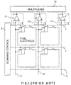
- FIG. 1 shows an active matrix circuit for a radiation imaging device, according to the prior art.
- a transducer (not shown) converts electromagnetic radiation into charge signal.
- the transducer can be, for example, a relatively thick (e.g. 500 ⁇ m) layer of amorphous selenium (a-Se) across which a high voltage may be applied between a top electrode on one side of the a-Se layer and the pixel electrodes 1 on the opposite side. Electron-hole pairs are generated in the a-Se layer in response to incident radiation, and the charges move toward the two electrodes under the influence of an electric field established by the high voltage.
- a-Se amorphous selenium
- the charge deposited on pixel electrodes 1 is then read out on a row-by-row basis by means of an array of thin film transistors (TFTs 3). Successive rows of pixel electrodes 1 are scanned in response to scanning control circuit 5 applying a scanning pulse to gate lines 7, to which the gate electrodes of successive rows of TFTs 3 are connected. Charges stored on each of the scanned rows of pixel electrodes 1, are applied to adjacent source or data lines 9 via the drain-source signal path through the associated TFTs 3. This signal is measured using charge amplifiers 11 connected to respective data or source lines 9.
- the charge amplifiers 11 may be of standard well known design.
- a multiplexer 13 is used to select successive outputs of the charge amplifiers 11. Additional A/D conversion circuitry (now shown) is provided to convert the sensed charges to digital signals for further processing, display, etc.
- the occupancy of the source or data lines 9 reduces the fill factor of each pixel in such prior art designs, unless an additional insulating layer is placed between the source lines and the pixel electrodes 1.
- the charge amplifiers 11 for such prior art read-out matrices usually suffer from a trade-off between sensitivity and dynamic range since a charge amplifier which has been designed for high sensitivity cannot measure large signals due to saturation of the response. Also, many wire bond connections must be made between the pixel array and the scanning control and charge amplifier circuits (usually silicon integrated circuits).
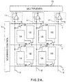
- FIG. 2A a first embodiment of the circuitry according to the present invention is shown.
- two pixel electrodes are provided for each space normally occupied by a single pixel in the prior art of Fig. 1.
- First pixel electrode 1A is connected to source line 9 via first TFT 3A, the gate input of which is connected to a first one of the control lines 7 on one side of the pixel.
- a second pixel electrode 1B is connected to first pixel electrode 1A via second TFT 3B, the gate input of which is connected to the other control line 7 for the pixel.
- the gate lines 7 are sequentially scanned, starting at the top and moving down.
- the charge carried on pixel electrodes 1A is read out through the TFTs 3A.
- the read-out process momentarily leaves pixel electrodes 1A free of charge.
- part of the charge carried by pixel electrodes 1B is transferred to the pixel electrodes 1A, through TFTs 3B. This charge is then read out when TFTs 3A are activated during the second successive scan of gate lines 7.
- the transfer of charge from pixel electrodes 1B to 1A is incomplete. Consequently, the signal derived from the pixel electrodes 1B in the second sequential scan of gate lines 7, must be multiplied by a suitable correction factor.
- the ratio of the total charge initially induced on pixel 1B to the charge measured on the second scan is given by (C1A + C1B)/C1A, where C1A and C1B are the storage capacitances of pixels 1A and 1B, respectively.
- pixels 1A are first read by successively addressing gate lines 7 as discussed above, from the top row down.
- the charge originally on the pixels 1B which is thereby redistributed between the pixels 1A and 1B is then read-out by simultaneously addressing adjacent gate lines 7 (i.e. two at a time), starting from the bottom and moving up. This allows the original charge on the pixels 1B to be read out completely, without the need for any multiplication factor.
- the circuit of Figure 2A can also be used to extend the dynamic range for charge read-out without changing the number of pixels per source line.
- pixel electrodes 1B are made smaller than pixel electrodes 1A and are placed sufficiently close to pixel electrodes 1A as to effectively sample the same radiation induced charge. Suitable area ratios 1A/1B could be anywhere from about 2 to 20. In this case, pixel electrodes 1A and 1B are considered to be components of the same pixel.
- the charges deposited on pixel electrodes 1A are read out. For some of the pixels, this charge may be enough to saturate the associated charge amplifiers 11.
- the charge from the smaller pixel electrodes 1B are sampled, which, in most cases, does not result in saturation of the associated charge amplifiers 11.
- data from the second scan multiplied by a suitable factor, is used.
- the signals on some pixels might be large enough to saturate the charge amplifiers 11 even on the second scan.
- a third or fourth scan can be used to further sub-divide the remaining charge until it is reduced to a measurable level.
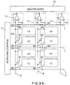
- FIG. 3A a second embodiment of the invention is shown in which a given number of pixels are addressed using only half the usual number of gate lines.
- pixel electrodes 1A are connected to source lines 9 as discussed above with reference to Figure 2.
- Second pixel electrodes 1C are also connected to source lines (i.e. data lines) 9, via series-connected TFTs 3C and 3D, the gate input of TFT 3C being connected to the top gate line or control line 7, while the gate input of TFT 3D is connected to the bottom control line (i.e. gate line) 7.
- the charge deposited on pixel electrodes 1A are read out by activating gate lines 7 one row at a time, in the usual manner. During this process, the charges on pixel electrodes 1C are not disturbed since at least one of the two TFTs 3C and 3D will be off for each pixel. The charges on pixel electrodes 1C are read out only after reading pixel electrodes 1A, by activating two adjacent gate lines 7 simultaneously.
- the circuit of Figure 3A can also be used to extend the dynamic range in a similar manner as discussed above with reference to Figure 2A.
- the pixel electrodes 1C are made smaller than pixel electrodes 1A and are placed very close to them, so as to effectively sample the same radiation induced charge.
- the signals from pixel electrodes 1A are normally used upon sequential scanning, unless saturation of the associated charge amplifiers 11 occurs. In the latter case, the signals from the smaller electrodes 1C, multiplied by a suitable correction factor, are used.
- this circuit only one level of dynamic range extension is possible since the charges on pixel electrodes 1C are read out completely, rather than being sub-divided on subsequent scans as in the embodiment of Figure 2A.
- FIG. 2A the pixels are located to the right of pixels 1A and the number of source lines (i.e. data lines) per pixel is reduced.
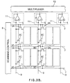
- this can be easily rearranged so that the pixels 1B are located beneath the pixels 1A as shown in Figure 2B, so that the number of gate lines (i.e. control lines) per pixel is reduced instead.
- the pixels 1C are shown disposed to the right of the pixels 1A, thereby reducing the number of source lines (i.e. data lines) per pixel, rather than the number of gate lines (i.e. control lines) per pixel as in Figure 3A.
- FIG. 2 The circuits of Figures 2 and 3 can be combined to reduce both the number of source lines per pixel and the number of gate lines per pixel, as shown in Figure 4.
- pixel electrodes 1A are read first by sequentially scanning the gate lines 7 from the top down.
- the main portion of charge on pixel electrodes 1B is read next by again sequentially scanning the gate lines 7, from the top down.
- pixel electrodes 1C are read by simultaneously addressing adjacent pairs of gate lines 7.
- the charge measured during this last step will contain a remnant of charge from pixel electrodes 1B. However, since the magnitude of this charge is known from the previous step of charge calculation, an equivalent amount can be subtracted from the charge sensed in this last step by post processing.
- the two transistors 3C and 3D may be replaced by a single thin film transistor having both upper and lower gates.
- Transistors 3C and 3D, and their alternative dual gate embodiments are shown in Figures 5a and 5b, respectively.
- the alterative embodiment provides an improved fill factor by reducing the number of transistors.
- the gate voltage levels for the ON and OFF state must be chosen so that transistor 3E is ON only if both upper and lower gates have ON voltages applied thereto.
- transistors 3A and 3B can be either single gate devices or dual date devices, with upper and lower gates connected together.
- a fourth pixel electrode 1D is provided for each pixel, this pixel electrode being connected to pixel electrode 1C via a further TFT switching transistor 3E.
- TFT switching transistor 3C' is fabricated as a dual gate device with top and bottom gates identified as G1 and G2, wherein the top gate is physically located above the channel and the bottom gate is located below the channel.
- the control lines 7 are successively scanned with a two level waveform, as shown in the left hand portion of Figure 6.
- a medium level gate voltage is first applied (e.g. 10 volts from a nominal OFF value of -5 volts), which causes the charge collected on pixels 1A to be read-out and cleared.
- the charges on pixels 1C are not transferred at this stage because the medium level gate voltage is insufficient to enable transistor 3C' while gate G2 is set to an OFF (i.e. -5 volts) voltage.
- the control pulse is then increased to a high level (e.g. 20 volts), which is sufficient to enable transistor 3C' so that the charge on pixels 1C is read-out, even though the low voltage (e.g - 5 volts) is still applied to gate G2.
- This medium-high pulse transition is applied successively to respective control lines 7, preferably from the top down.
- a portion of the charge originally deposited on the pixels 1B is transferred to the pixels 1A, and a portion of the charge originally deposited in the pixels 1D is transferred to the pixels 1C.
- These transferred charges are then read-out using a second scan of medium-high pulse transitions, again from the top down.
- the transistors 3C' are designed so that they turn on with a high voltage applied to gate G1 when a low voltage is applied to gate G2, but are disabled as long as a low voltage is applied to gate G1. This characteristic of the transistors 3C' is obtained by insuring that the gate G1 spans the entire length of the channel, while the gate G2 spans only a portion of the channel.
- the embodiment of Figure 6 reduces both the number of gates per pixel and the number of source lines per pixel.
- a versatile charge read-out matrix can be provided which is capable in one application of significantly increasing the pixel fill factor by reducing the number of source lines and gate lines, for example by one half over the prior art design of Fig. 1.
- the same circuits are capable of extending the dynamic range of the output charge amplifiers without compromising sensitivity.
- the dynamic range for read-out may be increased without reducing the number of source or gate lines.
Landscapes
- Engineering & Computer Science (AREA)
- Multimedia (AREA)
- Signal Processing (AREA)
- Solid State Image Pick-Up Elements (AREA)
- Transforming Light Signals Into Electric Signals (AREA)
Claims (35)
- Bilderfassungsanordnung, umfassend eine Anzahl in Zeilen und Spalten angeordneter Pixel (1), wobei jedes Pixel von mindestens einer Datenleitung (9) und mindestens zwei Steuerleitungen (7) begrenzt ist, die mit einer Ansprechsteuerschaltung (5) verbunden sind, dadurch gekennzeichnet, dass für jedes Pixel mindestens zwei Pixelelektroden (1A, 1B) vorhanden sind und mindestens zwei Schaltvorrichtungen (3A, 3B), wobei eine erste Pixelelektrode (1A) über eine erste Schaltvorrichtung (3A) mit der mindestens einen Datenleitung (9) verbunden ist, und ein Steuereingang der ersten Schaltvorrichtung (3A) an eine erste Steuerleitung (7) angeschlossen ist, so dass beim Empfang eines ersten Ansprechimpulses von der Ansprechsteuerschaltung (5) die Ladung auf der ersten Pixelelektrode (1A) auf die mindestens eine Datenleitung (9) übertragen wird, und eine zweite Pixelelektrode (1B) über eine zweite Schaltvorrichtung (3B) mit der ersten Pixelelektrode (1A) verbunden ist, und ein Steuereingang der zweiten Schaltvorrichtung (3B) mit einer zweiten Steuerleitung (7) verbunden ist, so dass beim Empfang eines zweiten Ansprechimpulses von der Steuerschaltung (5) nach einem ersten Ansprechimpuls die Ladung auf der zweiten Pixelelektrode (1B) auf die erste Pixelelektrode (1A) übertragen wird.
- Anordnung nach Anspruch 1, wobei jede Schaltvorrichtung (3A, 3B) einen Dünnfilmtransistor (TFT) enthält.
- Anordnung nach Anspruch 2, worin bei jedem Pixel ein Sourceanschluss der ersten Schaltvorrichtung (3A) mit der mindestens einen Datenleitung (9) verbunden ist, ein Gateanschluss mit der ersten Steuerleitung (7) verbunden ist und ein Drainanschluss mit der ersten Pixelelektrode (1A) verbunden ist.
- Anordnung nach Anspruch 2 oder 3, worin bei jedem Pixel ein Sourceanschluss der zweiten Schaltvorrichtung (3B) mit der ersten Pixelelektrode (1A) verbunden ist, ein Gateanschluss mit der zweiten Steuerleitung (7) verbunden ist und ein Drainanschluss mit der zweiten Pixelelektrode (1B) verbunden ist.
- Verfahren zum Betreiben einer Anordnung nach irgendeinem der Ansprüche 1 bis 4, umfassend die Schritte:a) das Anlegen eines ersten Ansprechimpulses aus der Ansprechsteuerschaltung (5) an den Steuereingang der ersten Schaltvorrichtung (3A), damit die Ladung auf der ersten Pixelelektrode (1A) auf die mindestens eine Datenleitung (9) übertragen wird; undb) nachdem die Ladung im Schritt a) auf die mindestens eine Datenleitung (9) übertragen worden ist, das Anlegen eines zweiten Ansprechimpulses aus der Ansprechsteuerschaltung (5) an den Steuereingang der zweiten Schaltvorrichtung (3B), damit die Ladung auf der zweiten Pixelelektrode (1B) auf die erste Pixelelektrode übertragen wird.
- Verfahren zum Betreiben einer Anordnung nach irgendeinem der Ansprüche 1 bis 4, umfassend die Schritte:a) das Ansprechen aufeinander folgender Steuerleitungen (7), so dass für jedes Pixel die Ladung, die die erste Pixelelektrode (1A) trägt, aufgrund des Ansprechens der ersten der mindestens zwei Steuerleitungen (7) auf die mindestens eine Datenleitung (9) übertragen wird, und ein Teil der Ladung, die die zweite Pixelelektrode (1B) trägt, aufgrund des Ansprechens der zweiten Steuerleitung (7) auf die erste Pixelelektrode (1A) übertragen wird;b) das nochmalige Ansprechen aufeinander folgender Steuerleitungen (7), so dass der Teil der Ladung, der von der zweiten Pixelelektrode (1B) auf die erste Pixelelektrode (1A) übertragen worden ist, auf die mindestens eine Datenleitung (9) übertragen wird; undc) das Multiplizieren des Ladungsteils, der auf die mindestens eine Datenleitung (9) übertragen wird, mit einem Korrekturfaktor, der dem Kapazitätsverhältnis zwischen der ersten und der zweiten Pixelelektrode (1A, 1B) proportional ist, wobei jedes der Pixel als Pixelpaar arbeitet, das durch die erste und zweite Pixelelektrode bestimmt ist.
- Verfahren nach Anspruch 6, zudem umfassend die Schritte des wiederholten weiteren Ansprechens aufeinander folgender Steuerleitungen (7), damit die Ladung von jeder zweiten Pixelelektrode (1B) abgeführt wird.
- Verfahren nach Anspruch 6, zudem umfassend den Schritt des gleichzeitigen Ansprechens aller Steuerleitungen (7), damit die Ladung von jeder zweiten Pixelelektrode (1B) abgeführt wird.
- Anordnung nach irgendeinem der Ansprüche 1 bis 4 oder Verfahren nach irgendeinem der Ansprüche 5 bis 8, wobei jede zweite Pixelelektrode (1B) kleiner ist als jede erste Pixelelektrode (1A).
- Verfahren zum Betreiben einer Anordnung nach Anspruch 9, umfassend die Schritte:a) das Ansprechen aufeinander folgender Steuerleitungen (7), so dass für jedes Pixel die Ladung, die die erste Pixelelektrode (1A) trägt, aufgrund des Ansprechens der ersten der mindestens zwei Steuerleitungen (7) auf die mindestens eine Datenleitung (9) übertragen wird, und ein Teil der Ladung, die die zweite Pixelelektrode (1B) trägt, aufgrund des Ansprechens der zweiten Steuerleitung (7) auf die erste Pixelelektrode (1A) übertragen wird;b) für jedes Pixel das Erfassen, ob die auf die mindestens eine Datenleitung (9) übertragene Ladung größer ist als eine vorgeschriebene Sättigungsmenge;c) das nochmalige Ansprechen aufeinander folgender Steuerleitungen (7), so dass der Teil der Ladung, der von der zweiten Pixelelektrode (1B) auf die erste Pixelelektrode (1A) übertragen worden ist, auf die mindestens eine Datenleitung (9) übertragen wird; undd) für jedes Pixel, bei dem die auf die mindestens eine Datenleitung (9) übertragene Ladung kleiner ist als die vorgeschriebene Sättigungsmenge, das Auswählen der Ladung für die Ausgabeerkennung, und für jedes Pixel, bei dem die auf die mindestens eine Datenleitung (9) übertragene Ladung größer ist als die vorgeschriebene Sättigungsmenge, das Multiplizieren des Ladungsteils, der von der zweiten Pixelelektrode (1B) auf die mindestens eine Datenleitung (9) übertragen wird, mit einem Korrekturfaktor, um eine Ladung zu gewinnen, die der auf der ersten Pixelelektrode (1A) gespeicherten Ladung äquivalent ist, wobei die erste und die zweite Pixelelektrode eine identische Ladung je Einheitsfläche aufweisen, und das Auswählen der äquivalenten Ladung für die Ausgabeerkennung, wodurch der Dynamikbereich der Pixel vergrößert wird.
- Verfahren zum Betreiben einer Anordnung nach irgendeinem der Ansprüche 1 bis 4, umfassend die Schritte:a) das Ansprechen aufeinander folgender Steuerleitungen (7), so dass für jedes Pixel die Ladung, die die erste Pixelelektrode (1A) trägt, aufgrund des Ansprechens der ersten der mindestens zwei Steuerleitungen (7) auf die mindestens eine Datenleitung (9) übertragen wird, und die Ladung, die die zweite Pixelelektrode (1B) trägt, durch das Ansprechen der zweiten Steuerleitung (7) auf die erste Pixelelektrode (1A) und die zweite Pixelelektrode (1B) umverteilt wird; undb) das nochmalige Ansprechen aufeinander folgender benachbarter Steuerleitungspaare (7), so dass die gesamte verbliebene Ladung auf der ersten und der zweiten Pixelelektrode (1A, 1B) auf die mindestens eine Datenleitung (9) übertragen wird.
- Bilderfassungsanordnung, umfassend eine Anzahl in Zeilen und Spalten angeordneter Pixel (1), wobei jedes Pixel von mindestens einer Datenleitung und mindestens zwei Steuerleitungen begrenzt ist, dadurch gekennzeichnet, dass für jedes Pixel mindestens zwei Pixelelektroden (1A, 1C) vorhanden sind und mindestens drei Schaltvorrichtungen (3A, 3C, 3D), wobei eine erste Pixelelektrode (1A) über eine erste Schaltvorrichtung (3A) mit der mindestens einen Datenleitung verbunden ist und ein Steuereingang der ersten Schaltvorrichtung (3A) an eine erste Steuerleitung (7) angeschlossen ist, eine zweite Pixelelektrode (1C) über die zweiten und dritten Schaltvorrichtungen (3C, 3D) mit der mindestens einen Datenleitung (9) verbunden ist, ein Steuereingang der zweiten Schaltvorrichtung (3C) mit der ersten Steuerleitung verbunden ist und ein Steuereingang der dritten Schaltvorrichtung (3D) mit der zweiten Steuerleitung (7) verbunden ist.
- Anordnung nach Anspruch 12, wobei jede Schaltvorrichtung (3A, 3C, 3D) einen Dünnfilmtransistor (TFT) enthält.
- Anordnung nach Anspruch 13, worin bei jedem Pixel ein Sourceanschluss der ersten Schaltvorrichtung (3A) mit der mindestens einen Datenleitung (9) verbunden ist, ein Gateanschluss mit der ersten Steuerleitung (7) verbunden ist und ein Drainanschluss mit der ersten Pixelelektrode (1A) verbunden ist.
- Anordnung nach Anspruch 13 oder 14, worin bei jedem Pixel der Sourceanschluss der zweiten Schaltvorrichtung (3C) mit der mindestens einen Datenleitung (9) verbunden ist, ein Gateanschluss mit der ersten Steuerleitung (7) verbunden ist und ein Drainanschluss mit einem Sourceanschluss der dritten Schaltvorrichtung (3D) verbunden ist, der Gateanschluss jeder dritten Schaltvorrichtung (3D) mit der zweiten Steuerleitung (7) verbunden ist und ein Drainanschluss mit der zweiten Pixelelektrode (1C) verbunden ist.
- Anordnung nach irgendeinem der Ansprüche 12 bis 15, wobei die zweite und die dritte Schaltvorrichtung (3C, 3D) als Dual-Gate-Vorrichtung integriert sind.
- Verfahren zum Betreiben einer Anordnung nach irgendeinem der Ansprüche 12 bis 16, umfassend die Schritte:a) das Ansprechen aufeinander folgender Steuerleitungen (7), so dass für jedes Pixel die Ladung, die die erste Pixelelektrode (1A) trägt, aufgrund des Ansprechens der ersten Steuerleitung des Steuerleitungspaars (7) auf die mindestens eine Datenleitung (9) übertragen wird; undb) das nochmalige Ansprechen aufeinander folgender benachbarter Steuerleitungspaare (7), so dass für jedes Pixel die Ladung, die die zweite Pixelelektrode (1C) trägt, durch das Ansprechen der benachbarten Steuerleitungspaare (7) auf die mindestens eine Datenleitung (9) übertragen wird, wobei jedes der Pixel als Pixelpaar arbeitet, das durch die erste und zweite Pixelelektrode bestimmt ist.
- Anordnung nach irgendeinem der Ansprüche 12 bis 16 oder Verfahren nach Anspruch 17, wobei jede zweite Pixelelektrode (1C) kleiner ist als jede erste Pixelelektrode (1A).
- Verfahren zum Betreiben einer Anordnung nach Anspruch 18 oder Verfahren nach Anspruch 18, umfassend die Schritte:a) das Ansprechen aufeinander folgender Steuerleitungen (7), so dass für jedes Pixel die Ladung, die die erste Pixelelektrode (1A) trägt, aufgrund des Ansprechens der ersten Steuerleitung (7) auf die mindestens eine Datenleitung (9) übertragen wird;b) für jedes Pixel das Erfassen, ob die auf die mindestens eine Datenleitung (9) übertragene Ladung größer ist als eine vorgeschriebene Sättigungsmenge;c) das nochmalige Ansprechen aufeinander folgender Steuerleitungspaare (7), so dass die Ladung, die die zweite Pixelelektrode (1C) trägt, auf die mindestens eine Datenleitung (9) übertragen wird; undd) für jedes Pixel, bei dem die von der ersten Pixelelektrode (1A) auf die mindestens eine Datenleitung (9) übertragene Ladung geringer ist als die vorbestimmte Sättigungsmenge, das Auswählen der Ladung für die Ausgabeerkennung, und für jedes Pixel, bei dem die von der ersten Pixelelektrode (1A) auf die mindestens eine Datenleitung (9) übertragene Ladung größer ist als die vorgeschriebene Sättigungsmenge, das Multiplizieren der von der zweiten Pixelelektrode (1C) auf die mindestens eine Datenleitung (9) übertragenen Ladung mit einem Korrekturfaktor, der dem Flächenverhältnis der ersten und der zweiten Pixelelektrode proportional ist, und das Auswählen der mit dem Korrekturfaktor multiplizierten Ladung für die Ausgabeerkennung, wodurch der Dynamikbereich eines jeden Pixels vergrößert wird.
- Bilderfassungsanordnung, umfassend eine Anzahl in Zeilen und Spalten angeordneter Pixel (1), wobei jedes Pixel von einer Datenleitung (9) und einem Steuerleitungspaar (7) begrenzt ist, dadurch gekennzeichnet, dass für jedes Pixel mindestens drei Pixelelektroden (1A, 1B, 1C) vorhanden sind und mindestens vier Schaltvorrichtungen (3A, 3B, 3C, 3D), wobei eine erste Pixelelektrode (1A) über eine erste Schaltvorrichtung (3A) mit der Datenleitung (9) verbunden ist und ein Steuereingang der ersten Schaltvorrichtung (3A) an eine erste Steuerleitung (7) angeschlossen ist, eine zweite Pixelelektrode (1B) über eine zweite Schaltvorrichtung (3B) mit der ersten Pixelelektrode (1A) verbunden ist, wobei ein Steuereingang der zweiten Schaltvorrichtung (3B) mit der anderen Steuerleitung (7) verbunden ist, eine dritte Pixelelektrode (1C) über die dritte und die vierte Schaltvorrichtung (3C, 3D) mit der Datenleitung (9) verbunden ist, und ein Steuereingang der dritten Schaltvorrichtung (3C) mit der ersten Steuerleitung (7) verbunden ist und ein Steuereingang der vierten Schaltvorrichtung (3D) mit der anderen Steuerleitung (7) verbunden ist.
- Anordnung nach Anspruch 20, wobei jede Schaltvorrichtung (3A, 3B, 3C, 3D) einen Dünnfilmtransistor (TFT) enthält.
- Anordnung nach Anspruch 21, worin bei jedem Pixel ein Sourceanschluss der ersten Schaltvorrichtung mit der Datenleitung (9) verbunden ist, ein Gateanschluss mit der ersten Steuerleitung (7) verbunden ist und ein Drainanschluss mit der ersten Pixelelektrode (1A) verbunden ist.
- Anordnung nach Anspruch 21 oder 22, worin bei jedem Pixel der Sourceanschluss der zweiten Schaltvorrichtung (3B) mit der Datenleitung (9) verbunden ist, ein Gateanschluss mit der ersten Steuerleitung (7) verbunden ist und ein Drainanschluss mit einem Sourceanschluss der vierten Schaltvorrichtung (3D) verbunden ist, ein Gateanschluss jeder vierten Schaltvorrichtung (3D) mit der anderen Steuerleitung (7) verbunden ist und ein Drainanschluss mit der dritten Pixelelektrode (1C) verbunden ist.
- Anordnung nach Anspruch 21, 22 oder 23, wobei für jedes Pixel ein Sourceanschluss der dritten Schaltvorrichtung (3C) mit der Datenleitung (9) verbunden ist, ein Gateanschluss mit der ersten Steuerleitung (7) verbunden ist und ein Drainanschluss mit einem Sourceanschluss der vierten Schaltvorrichtung (3D) verbunden ist, und ein Gateanschluss jeder vierten Schaltvorrichtung (3D) mit der anderen Steuerleitung (7) verbunden ist und ein Drainanschluss mit der dritten Pixelelektrode (1C) verbunden ist.
- Anordnung nach irgendeinem der Ansprüche 20 bis 24, wobei die dritte und die vierte Schaltvorrichtung (3C, 3D) als Dual-Gate-Vorrichtung integriert sind.
- Verfahren zum Betreiben einer Anordnung nach irgendeinem der Ansprüche 20 bis 25, umfassend die Schritte:a) das Ansprechen aufeinander folgender Steuerleitungen (7), so dass für jedes Pixel die Ladung, die die erste Pixelelektrode (1A) trägt, aufgrund des Ansprechens der ersten Steuerleitung des Steuerleitungspaars (7) auf die Datenleitung (9) übertragen wird, und ein Teil der Ladung, die die zweite Pixelelektrode (1B) trägt, aufgrund des Ansprechens der anderen Steuerleitung (7) auf die erste Pixelelektrode (1A) übertragen wird;b) das nochmalige Ansprechen aufeinander folgender Steuerleitungen (7), so dass der Teil der Ladung, der von der zweiten Pixelelektrode (1B) auf die erste Pixelelektrode (1A) übertragen worden ist, auf die Datenleitung (9) übertragen wird;c) das Multiplizieren des Ladungsteils, der auf die Datenleitung (9) übertragen wird, mit einem Korrekturfaktor, der dem Kapazitätsverhältnis zwischen der ersten und der zweiten Pixelelektrode (1A, 1B) proportional ist;d) das nochmalige Ansprechen aufeinander folgender benachbarter Steuerleitungspaare (7), so dass für jedes Pixel die Ladung, die die dritte Pixelelektrode (1C) trägt, aufgrund des Ansprechens der benachbarten Steuerleitungspaare (7) auf die Datenleitung (9) übertragen wird, wobei jedes Pixel wie zwei Pixelpaare wirkt, ein erstes Pixelpaar durch die erste und die zweite Pixelelektrode (1A, 1B) bestimmt ist und ein zweites Pixelpaar durch die erste und die dritte Pixelelektrode (1A, 1C) bestimmt ist; unde) das Subtrahieren des auf die Datenleitung (9) übertragenen Ladungsteils von der Ladung, die von der dritten Pixelelektrode auf die Datenleitung übertragen worden ist.
- Anordnung nach Anspruch 2, 3, 4, 13, 14, 15, 21, 22, 23 oder 24, Anordnung nach Anspruch 9 wenn abhängig von Anspruch 2, Anspruch 16 wenn abhängig von Anspruch 13 oder Anspruch 25 wenn abhängig von Anspruch 21, Verfahren nach Anspruch 5, 6, 7, 8, 9, 10 oder 11 wenn abhängig von Anspruch 2, Verfahren nach Anspruch 17, 18 oder 19 wenn abhängig von Anspruch 13 oder Verfahren nach Anspruch 26 wenn abhängig von Anspruch 21, wobei jeder Dünnfilmtransistor (TFT) eine Vorrichtung mit einem einzigen Gate ist.
- Anordnung nach Anspruch 2, 3, 4, 13, 14, 15, 21, 22, 23 oder 24, Anordnung nach Anspruch 9 wenn abhängig von Anspruch 2, Anspruch 16 wenn abhängig von Anspruch 13 oder Anspruch 25 wenn abhängig von Anspruch 21, Verfahren nach Anspruch 5, 6, 7, 8, 9, 10 oder 11 wenn abhängig von Anspruch 2, Verfahren nach Anspruch 17, 18 oder 19 wenn abhängig von Anspruch 13 oder Verfahren nach Anspruch 26 wenn abhängig von Anspruch 21, wobei jeder Dünnfilmtransistor (TFT) eine Dual-Gate-Vorrichtung ist.
- Bilderfassungsanordnung, umfassend eine Anzahl in Zeilen und Spalten angeordneter Pixel (1), wobei jedes Pixel von einer Datenleitung (9) und einem Steuerleitungspaar (7) begrenzt ist, dadurch gekennzeichnet, dass für jedes Pixel mindestens vier Pixelelektroden (1A, 1B, 1C, 1D) vorhanden sind und mindestens vier Schaltvorrichtungen (3A, 3B, 3C' , 3E), wobei eine erste Pixelelektrode (1A) über eine erste Schaltvorrichtung (3A) mit der Datenleitung (9) verbunden ist und ein Steuereingang der ersten Schaltvorrichtung (3A) an eine erste Steuerleitung (7) angeschlossen ist, eine zweite Pixelelektrode (1B) über eine zweite Schaltvorrichtung (3B) mit der ersten Pixelelektrode (1A) verbunden ist, und ein Steuereingang der zweiten Schaltvorrichtung (3B) mit der anderen Steuerleitung (7) verbunden ist, eine dritte Pixelelektrode (1C) über die dritte Schaltvorrichtung (3C') mit der Datenleitung (9) verbunden ist, ein erster Steuereingang der dritten Schaltvorrichtung (3C') mit der ersten Steuerleitung (7) verbunden ist und ein zweiter Steuereingang davon mit der anderen Steuerleitung (7) verbunden ist, und eine vierte Pixelelektrode (1D) über eine vierte Schaltvorrichtung (3E) mit der dritten Pixelelektrode (1C) verbunden ist, und ein Steuereingang der vierten Schaltvorrichtung (3E) mit der anderen Steuerleitung (7) verbunden ist.
- Anordnung nach Anspruch 29, wobei jede Schaltvorrichtung (3A, 3B, 3C', 3E) einen Dünnfilmtransistor (TFT) enthält.
- Anordnung nach Anspruch 30, worin bei jedem Pixel ein Sourceanschluss der ersten Schaltvorrichtung (3A) mit der Datenleitung (9) verbunden ist, ein Gateanschluss mit der ersten Steuerleitung (7) verbunden ist und ein Drainanschluss mit der ersten Pixelelektrode (1A) verbunden ist.
- Anordnung nach Anspruch 30 oder 31, worin bei jedem Pixel der Sourceanschluss der zweiten Schaltvorrichtung (3B) mit der ersten Pixelelektrode (1A) verbunden ist, ein Gateanschluss mit der anderen Steuerleitung (7) verbunden ist und ein Drainanschluss mit der zweiten Pixelelektrode (1B) verbunden ist.
- Anordnung nach Anspruch 30, 31 oder 32, wobei für jedes Pixel ein Sourceanschluss der dritten Schaltvorrichtung (3C') mit der Datenleitung (9) verbunden ist, ein erster Gateanschluss mit der ersten Steuerleitung (7) verbunden ist, ein zweiter Gateanschluss mit der anderen Steuerleitung (7) verbunden ist, und ein Drainanschluss mit der dritten Pixelelektrode (1C) verbunden ist.
- Anordnung nach Anspruch 30, 31, 32 oder 33, wobei für jedes Pixel ein Sourceanschluss der vierten Schaltvorrichtung (3E) mit der dritten Pixelelektrode (1C) verbunden ist, ein Gateanschluss mit der anderen Steuerleitung (7) verbunden ist, und ein Drainanschluss mit der vierten Pixelelektrode (1D) verbunden ist.
- Verfahren zum Betreiben einer Anordnung nach irgendeinem der Ansprüche 29 bis 34, umfassend die Schritte:a) das Ansprechen aufeinander folgender Steuerleitungen (7), indem man zuerst eine Spannung mit mittlerem Pegel an den Steuereingang einer jeden ersten Schaltvorrichtung (3A) anlegt, so dass die Ladung, die die erste Pixelelektrode (1A) trägt, für jedes angesprochene Pixel auf die Datenleitung (9) übertragen wird, und ein Teil der Ladung, die die zweite und die vierte Pixelelektrode (1B, 1D) tragen, für jedes dem angesprochenen Pixel benachbarte Pixel auf die erste bzw. dritte Pixelelektrode (1A, 1C) übertragen wird, und danach das Anlegen einer Spannung mit hohem Pegel an den Steuereingang der ersten Schaltvorrichtung (3A) und den ersten Steuereingang der dritten Schaltvorrichtung (3A), so dass die Ladung, die die dritte Pixelelektrode trägt, für jedes angesprochene Pixel auf die Datenleitung (9) übertragen wird; undb) das nochmalige Ansprechen aufeinander folgender Steuerleitungen (7), so dass der Ladungsteil, der von der zweiten und vierten Pixelelektrode (1B, 1D) auf die erste und dritte Pixelelektrode (1A, 1C) übertragen worden ist, der mindestens einen Datenleitung (9) zugeführt wird.
Applications Claiming Priority (1)
| Application Number | Priority Date | Filing Date | Title |
|---|---|---|---|
| PCT/CA1995/000202 WO1996031976A1 (en) | 1995-04-07 | 1995-04-07 | Read-out circuit for active matrix imaging arrays |
Publications (2)
| Publication Number | Publication Date |
|---|---|
| EP0819351A1 EP0819351A1 (de) | 1998-01-21 |
| EP0819351B1 true EP0819351B1 (de) | 2001-08-01 |
Family
ID=4173075
Family Applications (1)
| Application Number | Title | Priority Date | Filing Date |
|---|---|---|---|
| EP95915088A Expired - Lifetime EP0819351B1 (de) | 1995-04-07 | 1995-04-07 | Ausleseschaltung für eine bildmatrix mit aktiver matrix |
Country Status (6)
| Country | Link |
|---|---|
| US (2) | US6300977B1 (de) |
| EP (1) | EP0819351B1 (de) |
| JP (1) | JPH11503283A (de) |
| CA (1) | CA2216136C (de) |
| DE (1) | DE69522013T2 (de) |
| WO (1) | WO1996031976A1 (de) |
Families Citing this family (49)
| Publication number | Priority date | Publication date | Assignee | Title |
|---|---|---|---|---|
| DE19740612B4 (de) * | 1997-08-30 | 2005-10-13 | Fraunhofer-Gesellschaft zur Förderung der angewandten Forschung e.V. | Anordnung von Bildsensorelementen |
| US6437307B1 (en) | 1997-09-12 | 2002-08-20 | Fraunhofer-Gesellschaft Zur Forderung Zur Angewandten Forshung E.V. | Image detection member and assembly of image detection members |
| US6956605B1 (en) * | 1998-08-05 | 2005-10-18 | Canon Kabushiki Kaisha | Image pickup apparatus |
| US6870946B1 (en) | 1998-08-06 | 2005-03-22 | Secugen Corporation | Compact optical fingerprint capturing and recognition system |
| US6381347B1 (en) | 1998-11-12 | 2002-04-30 | Secugen | High contrast, low distortion optical acquistion system for image capturing |
| AU4603400A (en) | 1999-05-10 | 2000-11-21 | Yves Chartier | Energy selective detection systems |
| US6654057B1 (en) | 1999-06-17 | 2003-11-25 | Micron Technology, Inc. | Active pixel sensor with a diagonal active area |
| US6693670B1 (en) | 1999-07-29 | 2004-02-17 | Vision - Sciences, Inc. | Multi-photodetector unit cell |
| JP2001251557A (ja) * | 1999-12-27 | 2001-09-14 | Canon Inc | エリアセンサ、該エリアセンサを有する画像入力装置および該エリアセンサの駆動方法 |
| TWI282457B (en) * | 2000-04-06 | 2007-06-11 | Chi Mei Optoelectronics Corp | Liquid crystal display component with defect restore ability and restoring method of defect |
| EP1303978A4 (de) * | 2000-07-05 | 2006-08-09 | Vision Sciences Inc | Verfahren zur komprimierung des dynamikbereiches |
| JP4144193B2 (ja) * | 2000-10-25 | 2008-09-03 | ソニー株式会社 | 表示パネル、及びディスプレイ装置 |
| JP2004530286A (ja) * | 2000-11-27 | 2004-09-30 | ビジョン−サイエンシズ・インコーポレイテッド | イメージ・センサ内での雑音レベルの軽減 |
| KR100432490B1 (ko) | 2001-09-17 | 2004-05-22 | (주)니트 젠 | 광학식 지문취득 장치 |
| WO2003073159A1 (en) | 2002-02-20 | 2003-09-04 | Planar Systems, Inc. | Light sensitive display |
| US7009663B2 (en) | 2003-12-17 | 2006-03-07 | Planar Systems, Inc. | Integrated optical light sensitive active matrix liquid crystal display |
| US7053967B2 (en) | 2002-05-23 | 2006-05-30 | Planar Systems, Inc. | Light sensitive display |
| TW548615B (en) * | 2002-03-29 | 2003-08-21 | Chi Mei Optoelectronics Corp | Display panel having driver circuit with data line commonly used by three adjacent pixels |
| TW544942B (en) * | 2002-09-30 | 2003-08-01 | Hannstar Display Corp | Thin film transistor array substrate |
| US20080084374A1 (en) | 2003-02-20 | 2008-04-10 | Planar Systems, Inc. | Light sensitive display |
| KR100965580B1 (ko) * | 2003-08-21 | 2010-06-23 | 엘지디스플레이 주식회사 | 액정표시장치와 그의 구동방법 |
| US7773139B2 (en) | 2004-04-16 | 2010-08-10 | Apple Inc. | Image sensor with photosensitive thin film transistors |
| US7532187B2 (en) * | 2004-09-28 | 2009-05-12 | Sharp Laboratories Of America, Inc. | Dual-gate transistor display |
| KR101006450B1 (ko) * | 2004-08-03 | 2011-01-06 | 삼성전자주식회사 | 액정 표시 장치 |
| US7557355B2 (en) * | 2004-09-30 | 2009-07-07 | Canon Kabushiki Kaisha | Image pickup apparatus and radiation image pickup apparatus |
| KR100680469B1 (ko) | 2005-01-31 | 2007-02-08 | 매그나칩 반도체 유한회사 | 인접한 화소들 사이의 센싱노드들이 공유된 씨모스 이미지센서 |
| KR100665943B1 (ko) * | 2005-06-30 | 2007-01-09 | 엘지.필립스 엘시디 주식회사 | 유기전계 발광 디스플레이 장치 및 구동방법 |
| JP2007060070A (ja) * | 2005-08-23 | 2007-03-08 | Casio Comput Co Ltd | 画像読取装置及びその駆動制御方法 |
| US7714917B2 (en) * | 2005-08-30 | 2010-05-11 | Aptina Imaging Corporation | Method and apparatus providing a two-way shared storage gate on a four-way shared pixel |
| KR101160839B1 (ko) * | 2005-11-02 | 2012-07-02 | 삼성전자주식회사 | 액정 표시 장치 |
| TWI322401B (en) * | 2006-07-13 | 2010-03-21 | Au Optronics Corp | Liquid crystal display |
| US7755121B2 (en) * | 2007-08-23 | 2010-07-13 | Aptina Imaging Corp. | Imagers, apparatuses and systems utilizing pixels with improved optical resolution and methods of operating the same |
| JP2009204978A (ja) * | 2008-02-28 | 2009-09-10 | Sony Corp | El表示パネルモジュール、el表示パネル及び電子機器 |
| KR101595817B1 (ko) * | 2008-08-22 | 2016-02-22 | 삼성디스플레이 주식회사 | 액정 표시 장치 |
| KR101542511B1 (ko) * | 2008-12-24 | 2015-08-07 | 삼성디스플레이 주식회사 | 표시 장치 |
| EP2567287B1 (de) * | 2010-05-03 | 2019-08-21 | InVisage Technologies, Inc. | Vorrichtungen und verfahren zur erfassung hochauflösender bilder und videos |
| US9310923B2 (en) | 2010-12-03 | 2016-04-12 | Apple Inc. | Input device for touch sensitive devices |
| US8638320B2 (en) | 2011-06-22 | 2014-01-28 | Apple Inc. | Stylus orientation detection |
| US9329703B2 (en) | 2011-06-22 | 2016-05-03 | Apple Inc. | Intelligent stylus |
| US8928635B2 (en) | 2011-06-22 | 2015-01-06 | Apple Inc. | Active stylus |
| US9176604B2 (en) | 2012-07-27 | 2015-11-03 | Apple Inc. | Stylus device |
| US9557845B2 (en) | 2012-07-27 | 2017-01-31 | Apple Inc. | Input device for and method of communication with capacitive devices through frequency variation |
| US9652090B2 (en) | 2012-07-27 | 2017-05-16 | Apple Inc. | Device for digital communication through capacitive coupling |
| US10048775B2 (en) | 2013-03-14 | 2018-08-14 | Apple Inc. | Stylus detection and demodulation |
| US10845901B2 (en) | 2013-07-31 | 2020-11-24 | Apple Inc. | Touch controller architecture |
| US10061450B2 (en) | 2014-12-04 | 2018-08-28 | Apple Inc. | Coarse scan and targeted active mode scan for touch |
| US10474277B2 (en) | 2016-05-31 | 2019-11-12 | Apple Inc. | Position-based stylus communication |
| CN109755258B (zh) * | 2017-11-08 | 2021-02-19 | 元太科技工业股份有限公司 | 画素阵列基板与显示装置 |
| US12153764B1 (en) | 2020-09-25 | 2024-11-26 | Apple Inc. | Stylus with receive architecture for position determination |
Family Cites Families (10)
| Publication number | Priority date | Publication date | Assignee | Title |
|---|---|---|---|---|
| US4445117A (en) * | 1981-12-28 | 1984-04-24 | Hughes Aircraft Company | Transistorized focal plane having floating gate output nodes |
| JP2620240B2 (ja) * | 1987-06-10 | 1997-06-11 | 株式会社日立製作所 | 液晶表示装置 |
| US5151689A (en) * | 1988-04-25 | 1992-09-29 | Hitachi, Ltd. | Display device with matrix-arranged pixels having reduced number of vertical signal lines |
| US5063449A (en) * | 1988-11-18 | 1991-11-05 | Kabushiki Kaisha Toshiba | Solid-state image sensor employing a gate and diode for bias charge injection |
| JP2641802B2 (ja) * | 1990-12-27 | 1997-08-20 | 富士通株式会社 | 撮像装置 |
| EP0536964B1 (de) * | 1991-10-05 | 1998-03-18 | Fujitsu Limited | Aktive Flüssigkristall-Matrix-Anzeige mit verminderter Anzahl von Datenbusleitungen |
| US5401952A (en) * | 1991-10-25 | 1995-03-28 | Canon Kabushiki Kaisha | Signal processor having avalanche photodiodes |
| US5406332A (en) * | 1992-03-06 | 1995-04-11 | Canon Kabushiki Kaisha | Photoelectric converting device |
| WO1994008331A1 (en) * | 1992-10-06 | 1994-04-14 | Panocorp Display Systems | Drive system and method for panel displays |
| JPH06334920A (ja) * | 1993-03-23 | 1994-12-02 | Nippon Hoso Kyokai <Nhk> | 固体撮像素子とその駆動方法 |
-
1995
- 1995-04-07 JP JP8529808A patent/JPH11503283A/ja not_active Abandoned
- 1995-04-07 WO PCT/CA1995/000202 patent/WO1996031976A1/en not_active Ceased
- 1995-04-07 CA CA002216136A patent/CA2216136C/en not_active Expired - Fee Related
- 1995-04-07 US US08/930,749 patent/US6300977B1/en not_active Expired - Fee Related
- 1995-04-07 DE DE69522013T patent/DE69522013T2/de not_active Expired - Fee Related
- 1995-04-07 EP EP95915088A patent/EP0819351B1/de not_active Expired - Lifetime
-
2001
- 2001-05-02 US US09/847,423 patent/US20010028481A1/en not_active Abandoned
Also Published As
| Publication number | Publication date |
|---|---|
| DE69522013T2 (de) | 2002-03-28 |
| US6300977B1 (en) | 2001-10-09 |
| EP0819351A1 (de) | 1998-01-21 |
| JPH11503283A (ja) | 1999-03-23 |
| CA2216136A1 (en) | 1996-10-10 |
| US20010028481A1 (en) | 2001-10-11 |
| WO1996031976A1 (en) | 1996-10-10 |
| DE69522013D1 (de) | 2001-09-06 |
| CA2216136C (en) | 2003-09-16 |
Similar Documents
| Publication | Publication Date | Title |
|---|---|---|
| US6300977B1 (en) | Read-out circuit for active matrix imaging arrays | |
| USRE42157E1 (en) | Photoelectric converter, its driving method, and system including the photoelectric converter | |
| EP0778983B1 (de) | Bildwandlersystem | |
| US6232607B1 (en) | High resolution flat panel for radiation imaging | |
| US7375748B2 (en) | Differential readout from pixels in CMOS sensor | |
| EP0653881B1 (de) | Festkörperbildaufnahmevorrichtung | |
| EP0922943B1 (de) | Strahlungsdetektor und Verfahren zur Strahlungsdetektion | |
| US6449014B1 (en) | Image sensor having a low impedance reading block between pixel data lines and output line | |
| EP0842539B1 (de) | Methode und apparat zum betrieb eines dual-gatter-tft-elektromagnetischen strahlungsbildwandlers | |
| US6486470B2 (en) | Compensation circuit for use in a high resolution amplified flat panel for radiation imaging | |
| US6940552B1 (en) | Photoelectric conversion device | |
| JP3039989B2 (ja) | 放射線撮像装置 | |
| JP2006148901A (ja) | 光電変換装置、放射線読取装置及び光電変換装置の駆動方法 | |
| Zarnowski et al. | Performance of a large-format charge-injection device | |
| JP2001320038A (ja) | 光電変換装置 | |
| JP2001074552A (ja) | 光電変換装置及びその駆動方法 | |
| JP2002033959A (ja) | 光電変換装置及びその駆動方法、放射線撮像システム | |
| JP2009005374A (ja) | 光電変換装置の駆動方法 | |
| CA2228153A1 (en) | Method and apparatus of operating a dual gate tft electromagnetic radiation imaging device | |
| JPH0477171A (ja) | リニアイメージセンサ |
Legal Events
| Date | Code | Title | Description |
|---|---|---|---|
| PUAI | Public reference made under article 153(3) epc to a published international application that has entered the european phase |
Free format text: ORIGINAL CODE: 0009012 |
|
| 17P | Request for examination filed |
Effective date: 19971103 |
|
| AK | Designated contracting states |
Kind code of ref document: A1 Designated state(s): DE FR GB NL |
|
| RAP1 | Party data changed (applicant data changed or rights of an application transferred) |
Owner name: LITTON SYSTEMS CANADA LIMITED |
|
| RAP1 | Party data changed (applicant data changed or rights of an application transferred) |
Owner name: 1294339 ONTARIO, INC. |
|
| GRAG | Despatch of communication of intention to grant |
Free format text: ORIGINAL CODE: EPIDOS AGRA |
|
| RAP1 | Party data changed (applicant data changed or rights of an application transferred) |
Owner name: IFIRE TECHNOLOGY INC. |
|
| 17Q | First examination report despatched |
Effective date: 20001121 |
|
| GRAG | Despatch of communication of intention to grant |
Free format text: ORIGINAL CODE: EPIDOS AGRA |
|
| GRAH | Despatch of communication of intention to grant a patent |
Free format text: ORIGINAL CODE: EPIDOS IGRA |
|
| GRAH | Despatch of communication of intention to grant a patent |
Free format text: ORIGINAL CODE: EPIDOS IGRA |
|
| GRAA | (expected) grant |
Free format text: ORIGINAL CODE: 0009210 |
|
| AK | Designated contracting states |
Kind code of ref document: B1 Designated state(s): DE FR GB NL |
|
| REF | Corresponds to: |
Ref document number: 69522013 Country of ref document: DE Date of ref document: 20010906 |
|
| ET | Fr: translation filed | ||
| REG | Reference to a national code |
Ref country code: GB Ref legal event code: IF02 |
|
| PGFP | Annual fee paid to national office [announced via postgrant information from national office to epo] |
Ref country code: FR Payment date: 20020327 Year of fee payment: 8 |
|
| PGFP | Annual fee paid to national office [announced via postgrant information from national office to epo] |
Ref country code: NL Payment date: 20020403 Year of fee payment: 8 |
|
| PLBE | No opposition filed within time limit |
Free format text: ORIGINAL CODE: 0009261 |
|
| STAA | Information on the status of an ep patent application or granted ep patent |
Free format text: STATUS: NO OPPOSITION FILED WITHIN TIME LIMIT |
|
| 26N | No opposition filed | ||
| PG25 | Lapsed in a contracting state [announced via postgrant information from national office to epo] |
Ref country code: NL Free format text: LAPSE BECAUSE OF NON-PAYMENT OF DUE FEES Effective date: 20031101 |
|
| NLV4 | Nl: lapsed or anulled due to non-payment of the annual fee |
Effective date: 20031101 |
|
| PG25 | Lapsed in a contracting state [announced via postgrant information from national office to epo] |
Ref country code: FR Free format text: LAPSE BECAUSE OF NON-PAYMENT OF DUE FEES Effective date: 20031231 |
|
| REG | Reference to a national code |
Ref country code: FR Ref legal event code: ST |
|
| REG | Reference to a national code |
Ref country code: GB Ref legal event code: 732E |
|
| PGFP | Annual fee paid to national office [announced via postgrant information from national office to epo] |
Ref country code: GB Payment date: 20060406 Year of fee payment: 12 |
|
| PGFP | Annual fee paid to national office [announced via postgrant information from national office to epo] |
Ref country code: DE Payment date: 20060419 Year of fee payment: 12 |
|
| GBPC | Gb: european patent ceased through non-payment of renewal fee |
Effective date: 20070407 |
|
| PG25 | Lapsed in a contracting state [announced via postgrant information from national office to epo] |
Ref country code: DE Free format text: LAPSE BECAUSE OF NON-PAYMENT OF DUE FEES Effective date: 20071101 |
|
| PG25 | Lapsed in a contracting state [announced via postgrant information from national office to epo] |
Ref country code: GB Free format text: LAPSE BECAUSE OF NON-PAYMENT OF DUE FEES Effective date: 20070407 |