EP0819783A1 - Procédé et appareillage pour préparer un monocristal - Google Patents
Procédé et appareillage pour préparer un monocristal Download PDFInfo
- Publication number
- EP0819783A1 EP0819783A1 EP97111715A EP97111715A EP0819783A1 EP 0819783 A1 EP0819783 A1 EP 0819783A1 EP 97111715 A EP97111715 A EP 97111715A EP 97111715 A EP97111715 A EP 97111715A EP 0819783 A1 EP0819783 A1 EP 0819783A1
- Authority
- EP
- European Patent Office
- Prior art keywords
- inner chamber
- inert gas
- single crystal
- chamber
- crucible
- Prior art date
- Legal status (The legal status is an assumption and is not a legal conclusion. Google has not performed a legal analysis and makes no representation as to the accuracy of the status listed.)
- Granted
Links
- 239000013078 crystal Substances 0.000 title claims abstract description 37
- 238000000034 method Methods 0.000 title claims abstract description 15
- 239000011261 inert gas Substances 0.000 claims abstract description 51
- 239000000155 melt Substances 0.000 claims abstract description 15
- 238000010438 heat treatment Methods 0.000 claims abstract description 10
- 229910052710 silicon Inorganic materials 0.000 claims abstract description 6
- 239000010703 silicon Substances 0.000 claims abstract description 6
- 238000004519 manufacturing process Methods 0.000 claims abstract description 4
- XUIMIQQOPSSXEZ-UHFFFAOYSA-N Silicon Chemical compound [Si] XUIMIQQOPSSXEZ-UHFFFAOYSA-N 0.000 claims abstract 4
- 238000009413 insulation Methods 0.000 claims description 17
- QVGXLLKOCUKJST-UHFFFAOYSA-N atomic oxygen Chemical compound [O] QVGXLLKOCUKJST-UHFFFAOYSA-N 0.000 claims description 11
- 229910052760 oxygen Inorganic materials 0.000 claims description 11
- 239000001301 oxygen Substances 0.000 claims description 11
- VYPSYNLAJGMNEJ-UHFFFAOYSA-N Silicium dioxide Chemical compound O=[Si]=O VYPSYNLAJGMNEJ-UHFFFAOYSA-N 0.000 description 12
- 229910052814 silicon oxide Inorganic materials 0.000 description 10
- OKTJSMMVPCPJKN-UHFFFAOYSA-N Carbon Chemical compound [C] OKTJSMMVPCPJKN-UHFFFAOYSA-N 0.000 description 6
- 229910002804 graphite Inorganic materials 0.000 description 5
- 239000010439 graphite Substances 0.000 description 5
- 238000012423 maintenance Methods 0.000 description 5
- 238000010348 incorporation Methods 0.000 description 4
- 239000007789 gas Substances 0.000 description 3
- 239000000203 mixture Substances 0.000 description 3
- 239000002245 particle Substances 0.000 description 3
- 238000010926 purge Methods 0.000 description 2
- 229910052799 carbon Inorganic materials 0.000 description 1
- 239000012159 carrier gas Substances 0.000 description 1
- 238000010276 construction Methods 0.000 description 1
- 238000013461 design Methods 0.000 description 1
- 239000000428 dust Substances 0.000 description 1
- 238000011010 flushing procedure Methods 0.000 description 1
- 238000009434 installation Methods 0.000 description 1
- 239000000289 melt material Substances 0.000 description 1
- 238000010943 off-gassing Methods 0.000 description 1
- 239000002244 precipitate Substances 0.000 description 1
- 239000010453 quartz Substances 0.000 description 1
- 230000005855 radiation Effects 0.000 description 1
- HBMJWWWQQXIZIP-UHFFFAOYSA-N silicon carbide Chemical compound [Si+]#[C-] HBMJWWWQQXIZIP-UHFFFAOYSA-N 0.000 description 1
- 229910010271 silicon carbide Inorganic materials 0.000 description 1
- 239000007787 solid Substances 0.000 description 1
- 230000002123 temporal effect Effects 0.000 description 1
- 238000012360 testing method Methods 0.000 description 1
- 238000004804 winding Methods 0.000 description 1
Images

Classifications
-
- C—CHEMISTRY; METALLURGY
- C30—CRYSTAL GROWTH
- C30B—SINGLE-CRYSTAL GROWTH; UNIDIRECTIONAL SOLIDIFICATION OF EUTECTIC MATERIAL OR UNIDIRECTIONAL DEMIXING OF EUTECTOID MATERIAL; REFINING BY ZONE-MELTING OF MATERIAL; PRODUCTION OF A HOMOGENEOUS POLYCRYSTALLINE MATERIAL WITH DEFINED STRUCTURE; SINGLE CRYSTALS OR HOMOGENEOUS POLYCRYSTALLINE MATERIAL WITH DEFINED STRUCTURE; AFTER-TREATMENT OF SINGLE CRYSTALS OR A HOMOGENEOUS POLYCRYSTALLINE MATERIAL WITH DEFINED STRUCTURE; APPARATUS THEREFOR
- C30B15/00—Single-crystal growth by pulling from a melt, e.g. Czochralski method
- C30B15/14—Heating of the melt or the crystallised materials
-
- C—CHEMISTRY; METALLURGY
- C30—CRYSTAL GROWTH
- C30B—SINGLE-CRYSTAL GROWTH; UNIDIRECTIONAL SOLIDIFICATION OF EUTECTIC MATERIAL OR UNIDIRECTIONAL DEMIXING OF EUTECTOID MATERIAL; REFINING BY ZONE-MELTING OF MATERIAL; PRODUCTION OF A HOMOGENEOUS POLYCRYSTALLINE MATERIAL WITH DEFINED STRUCTURE; SINGLE CRYSTALS OR HOMOGENEOUS POLYCRYSTALLINE MATERIAL WITH DEFINED STRUCTURE; AFTER-TREATMENT OF SINGLE CRYSTALS OR A HOMOGENEOUS POLYCRYSTALLINE MATERIAL WITH DEFINED STRUCTURE; APPARATUS THEREFOR
- C30B15/00—Single-crystal growth by pulling from a melt, e.g. Czochralski method
-
- Y—GENERAL TAGGING OF NEW TECHNOLOGICAL DEVELOPMENTS; GENERAL TAGGING OF CROSS-SECTIONAL TECHNOLOGIES SPANNING OVER SEVERAL SECTIONS OF THE IPC; TECHNICAL SUBJECTS COVERED BY FORMER USPC CROSS-REFERENCE ART COLLECTIONS [XRACs] AND DIGESTS
- Y10—TECHNICAL SUBJECTS COVERED BY FORMER USPC
- Y10T—TECHNICAL SUBJECTS COVERED BY FORMER US CLASSIFICATION
- Y10T117/00—Single-crystal, oriented-crystal, and epitaxy growth processes; non-coating apparatus therefor
- Y10T117/10—Apparatus
- Y10T117/1024—Apparatus for crystallization from liquid or supercritical state
- Y10T117/1076—Apparatus for crystallization from liquid or supercritical state having means for producing a moving solid-liquid-solid zone
- Y10T117/1088—Apparatus for crystallization from liquid or supercritical state having means for producing a moving solid-liquid-solid zone including heating or cooling details
Definitions
- the invention relates to a method for producing a Single crystal made of silicon in a pull-in chamber flushed with inert gas by pulling the single crystal out of a melt the Czochralski method.
- the invention also relates a device for performing the method.
- the silicon oxide remaining in the melt causes the incorporation of oxygen into the single crystal.
- a connection that is used to control the Incorporation of oxygen in the single crystal is used.
- Silicon oxide strikes the heater used for heating the crucible and usually made of graphite, a layer soon forms made of silicon carbide that covers the surface of the heater covered. This layer becomes brittle over time and becomes one Source of unwanted particles. The same thing happens when the insulation surrounding the heater with silicon oxide responds. This can also affect the insulation behavior change the insulation so much that pulling one Einkistalls is no longer possible because of the prerequisites for single crystal crystal growth in terms of the temperature field in the melt and in the single crystal is not have more fulfilled. It is therefore imperative that the device for producing single crystals regularly is shut down and cleaned, and that damaged parts of the Device to be replaced. However, such maintenance work is complex and associated with very high costs.
- the object of the invention was to extend the Operating times between two necessary maintenance tasks achieve without having to accept disadvantages.
- the invention also relates to a device for carrying it out of the procedure.
- the device is marked through a first inner chamber in which the crucible and the Heat shield and through a second inner chamber, in which is the heater, with the inner chambers are limited by side, ceiling and floor boundaries; and by a first means for supplying inert gas through the ceiling of the first inner chamber into the first inner chamber and through a second device for feeding of inert gas by limiting the bottom of the second inner Chamber in the second inner chamber.
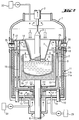
- the device according to Figure 1 comprises a drawing chamber 1 with a only hinted device 2 for pulling a Single crystal 3 from a melt 4 according to the Czochralski method.
- the melt is in a crucible 5a usually consists of quartz glass, from a support crucible 5b is supported and rotatable on a shaft 6 and vertically is slidably mounted.
- a heat shield 7 which surrounds the single crystal and comes close to the surface of the Melt reaches.
- the heat shield can be tubular or, as can be seen from Figure 1, conical be.
- To support the heat shield is in the upper part the drawing system a bracket 8 is provided.
- a heater 9 is arranged around the crucible 5a around and below the crucible.
- a resistance heater is usually used as the heating device made of graphite with at least one power supply 10 used.
- the drawing chamber is more damaging due to insulation Protected against heat.
- Insulation 11 is around arranged the heater around. It includes, for example a radiation tube 11a made of graphite and a winding 11b made of graphite felt. Further insulation 12 and 13 are located in the lower part of the drawing chamber 1.
- the interior is the Drawing chamber below the holder 8 for the heat shield 7 divided by further internals into inner chambers.
- the first inner chamber 14 is laterally delimited by a tube 16.
- Further limitations form the bracket 8 (ceiling of the chamber 14) and a support plate 17 (floor boundary of the chamber 14).
- the tube 16 and the carrier plate 17 are preferably made of graphite manufactured and also act as limitations the second inner chamber 15.
- Further limitations of the second inner chamber 15 form the cover 18 (ceiling delimitation the chamber 15), the insulation 13 (floor limitation the chamber 15) and a support tube 20 and the insulation 11 (Side boundaries of chamber 15).
- Each of the inner chambers 14 and 15 has its own Device for supplying inert gas.
- the device 22 for Feeding inert gas into the first inner chamber 14 sends an inert gas flow I in the upper part of the drawing chamber and through the bracket 8 and through the heat shield 7 in the first inner chamber 14.
- the supplied inert gas stream leaves the inner Chamber 14 through outlet openings 23 in the tube 16 and through Outlet openings 24 of a deflecting tube 25.
- the supplied inert gas through suction openings 28 from the drawing chamber 1 sucked.
- the device 29 for supplying inert gas in the second inner chamber 15 sends an inert gas stream II through the bottom 19 of the drawing chamber 1 and the insulation 13 in the second inner chamber 15.
- the supplied inert gas stream leaves the inner chamber 15 through outlet openings 26 in the cover 18 and is also made through the suction openings 28 the drawing chamber 1 sucked.
- the inert gas flows can at the earliest after leaving of the inner chambers 14 and 15 mix. In the shown This embodiment takes place in a suction chamber 27 which communicates with the suction openings 28.
- the featured Construction of the device precludes the Inert gas stream I, which is loaded with silicon oxide, in particular get to the heater 9 and insulation 11 can.
- the inert gas stream II prevents 11 deposits form on the insulation and thus the risk electrical arcing increases.
- FIG. 2 shows a further embodiment of the invention, which relates to the embodiment to which FIG. 1 relates, distinguished by an additional feature.
- the device has a third device 30 for feeding Inert gas on an inert gas flow III through the support plate 17 sends into the first inner chamber 14.
- the fed Inert gas stream III leaves the inner chamber 14 through the Outlet openings 23 in the tube 16 and through the outlet openings 24 in the deflection tube 25 and is through the suction openings 28 the drawing chamber 1 sucked. Mix the inert gas streams I and III already in the inner chamber 14.
- the incorporation of oxygen in the single crystal not only by supplying the inert gas stream I, but also by supplying the inert gas stream III influenced.
- An important variable through which the installation controlled by oxygen is the amount of inert gas the per unit time via the inert gas streams I and III is passed through the inner chamber 14. You must during the Pulling the single crystal can be changed in a controlled way reaches a certain oxygen concentration in the single crystal becomes. As a rule, the oxygen concentration in the Single crystal does not exceed a desired, narrow range of values fall below.
Landscapes
- Chemical & Material Sciences (AREA)
- Engineering & Computer Science (AREA)
- Crystallography & Structural Chemistry (AREA)
- Materials Engineering (AREA)
- Metallurgy (AREA)
- Organic Chemistry (AREA)
- Crystals, And After-Treatments Of Crystals (AREA)
Applications Claiming Priority (2)
| Application Number | Priority Date | Filing Date | Title |
|---|---|---|---|
| DE19628851A DE19628851A1 (de) | 1996-07-17 | 1996-07-17 | Verfahren und Vorrichtung zur Herstellung eines Einkristalls |
| DE19628851 | 1996-07-17 |
Publications (2)
| Publication Number | Publication Date |
|---|---|
| EP0819783A1 true EP0819783A1 (fr) | 1998-01-21 |
| EP0819783B1 EP0819783B1 (fr) | 2000-09-20 |
Family
ID=7800096
Family Applications (1)
| Application Number | Title | Priority Date | Filing Date |
|---|---|---|---|
| EP97111715A Expired - Lifetime EP0819783B1 (fr) | 1996-07-17 | 1997-07-10 | Procédé et appareillage pour préparer un monocristal |
Country Status (7)
| Country | Link |
|---|---|
| US (1) | US5746824A (fr) |
| EP (1) | EP0819783B1 (fr) |
| JP (1) | JP3000141B2 (fr) |
| KR (1) | KR100284572B1 (fr) |
| DE (2) | DE19628851A1 (fr) |
| MY (1) | MY133687A (fr) |
| TW (1) | TW476816B (fr) |
Cited By (5)
| Publication number | Priority date | Publication date | Assignee | Title |
|---|---|---|---|---|
| WO2000020664A1 (fr) * | 1998-10-07 | 2000-04-13 | Memc Electronic Materials, Inc. | Procede d'oxydation continue pour appareil de tirage du cristal |
| CN101509148B (zh) * | 2008-02-15 | 2011-05-25 | 绿能科技股份有限公司 | 具有泄浆导流结构的长晶炉 |
| CN102758258A (zh) * | 2012-06-20 | 2012-10-31 | 合肥景坤新能源有限公司 | 单晶炉用伸展式热屏蔽器 |
| CN105177701A (zh) * | 2015-10-14 | 2015-12-23 | 江苏华盛天龙光电设备股份有限公司 | 一种低能耗单晶炉 |
| CN107779946A (zh) * | 2016-08-25 | 2018-03-09 | 上海新昇半导体科技有限公司 | 热屏组件及单晶提拉炉热场结构 |
Families Citing this family (14)
| Publication number | Priority date | Publication date | Assignee | Title |
|---|---|---|---|---|
| JP3826472B2 (ja) * | 1996-02-08 | 2006-09-27 | 株式会社Sumco | 単結晶製造装置およびこれを使用した単結晶製造方法 |
| US6254673B1 (en) * | 1999-12-07 | 2001-07-03 | Seh America, Inc. | Auxillary vacuum apparatus and method for crystal growth |
| US6482263B1 (en) * | 2000-10-06 | 2002-11-19 | Memc Electronic Materials, Inc. | Heat shield assembly for crystal pulling apparatus |
| KR20030055900A (ko) * | 2001-12-27 | 2003-07-04 | 주식회사 실트론 | 단결정 잉곳의 제조장치 |
| TW200928018A (en) * | 2007-12-21 | 2009-07-01 | Green Energy Technology Inc | Crystal-growing furnace with convectional cooling structure |
| CN101481825B (zh) * | 2008-01-08 | 2010-11-17 | 绿能科技股份有限公司 | 具有对流式散热构造的长晶炉 |
| CN101519801B (zh) * | 2008-02-26 | 2011-10-12 | 绿能科技股份有限公司 | 长晶炉体结构 |
| KR101111681B1 (ko) * | 2010-10-05 | 2012-02-14 | (주)기술과가치 | 단결정 실리콘 잉곳 제조장치 |
| JP2013053017A (ja) * | 2011-09-01 | 2013-03-21 | Shin Etsu Handotai Co Ltd | 単結晶育成装置 |
| TWI461359B (zh) * | 2011-09-23 | 2014-11-21 | Masahiro Hoshino | Low energy consumption and high efficiency metal silicon purification device |
| DE112017001711B4 (de) * | 2016-03-29 | 2022-05-19 | Corner Star Limited | Kristallzüchtungsvorrichtung und diesbezügliche Verfahren |
| JP7259242B2 (ja) * | 2018-09-27 | 2023-04-18 | 住友金属鉱山株式会社 | ニオブ酸リチウム単結晶の製造方法 |
| CN110592661A (zh) * | 2019-09-11 | 2019-12-20 | 上海新昇半导体科技有限公司 | 一种晶体生长装置 |
| CN113755944A (zh) * | 2020-06-05 | 2021-12-07 | 西安奕斯伟材料科技有限公司 | 一种单晶炉热场结构、单晶炉及晶棒 |
Citations (4)
| Publication number | Priority date | Publication date | Assignee | Title |
|---|---|---|---|---|
| JPS61158890A (ja) * | 1984-12-28 | 1986-07-18 | Fujitsu Ltd | 結晶成長装置 |
| EP0568183A1 (fr) * | 1992-03-31 | 1993-11-03 | Shin-Etsu Handotai Company Limited | Appareil pour tirer un monocristal de silicium |
| EP0608875A1 (fr) * | 1993-01-28 | 1994-08-03 | Mitsubishi Materials Silicon Corporation | Système pour le tirage d'un monocrystal et procédé pour l'aspiration de l'oxyde de silicium |
| EP0715005A1 (fr) * | 1994-12-01 | 1996-06-05 | Wacker Siltronic Gesellschaft für Halbleitermaterialien mbH | Dispositif et procédé pour produire un monocristal |
Family Cites Families (1)
| Publication number | Priority date | Publication date | Assignee | Title |
|---|---|---|---|---|
| US5363796A (en) * | 1991-02-20 | 1994-11-15 | Sumitomo Metal Industries, Ltd. | Apparatus and method of growing single crystal |
-
1996
- 1996-07-17 DE DE19628851A patent/DE19628851A1/de not_active Withdrawn
-
1997
- 1997-06-10 US US08/872,566 patent/US5746824A/en not_active Expired - Lifetime
- 1997-07-04 MY MYPI97003034A patent/MY133687A/en unknown
- 1997-07-10 EP EP97111715A patent/EP0819783B1/fr not_active Expired - Lifetime
- 1997-07-10 DE DE59702373T patent/DE59702373D1/de not_active Expired - Lifetime
- 1997-07-11 KR KR1019970032332A patent/KR100284572B1/ko not_active Expired - Lifetime
- 1997-07-14 JP JP9188460A patent/JP3000141B2/ja not_active Expired - Lifetime
- 1997-07-16 TW TW086110110A patent/TW476816B/zh not_active IP Right Cessation
Patent Citations (4)
| Publication number | Priority date | Publication date | Assignee | Title |
|---|---|---|---|---|
| JPS61158890A (ja) * | 1984-12-28 | 1986-07-18 | Fujitsu Ltd | 結晶成長装置 |
| EP0568183A1 (fr) * | 1992-03-31 | 1993-11-03 | Shin-Etsu Handotai Company Limited | Appareil pour tirer un monocristal de silicium |
| EP0608875A1 (fr) * | 1993-01-28 | 1994-08-03 | Mitsubishi Materials Silicon Corporation | Système pour le tirage d'un monocrystal et procédé pour l'aspiration de l'oxyde de silicium |
| EP0715005A1 (fr) * | 1994-12-01 | 1996-06-05 | Wacker Siltronic Gesellschaft für Halbleitermaterialien mbH | Dispositif et procédé pour produire un monocristal |
Non-Patent Citations (1)
| Title |
|---|
| PATENT ABSTRACTS OF JAPAN vol. 10, no. 362 (C - 389)<2419> 4 December 1986 (1986-12-04) * |
Cited By (6)
| Publication number | Priority date | Publication date | Assignee | Title |
|---|---|---|---|---|
| WO2000020664A1 (fr) * | 1998-10-07 | 2000-04-13 | Memc Electronic Materials, Inc. | Procede d'oxydation continue pour appareil de tirage du cristal |
| US6315828B1 (en) | 1998-10-07 | 2001-11-13 | Memc Electronic Materials, Inc. | Continuous oxidation process for crystal pulling apparatus |
| CN101509148B (zh) * | 2008-02-15 | 2011-05-25 | 绿能科技股份有限公司 | 具有泄浆导流结构的长晶炉 |
| CN102758258A (zh) * | 2012-06-20 | 2012-10-31 | 合肥景坤新能源有限公司 | 单晶炉用伸展式热屏蔽器 |
| CN105177701A (zh) * | 2015-10-14 | 2015-12-23 | 江苏华盛天龙光电设备股份有限公司 | 一种低能耗单晶炉 |
| CN107779946A (zh) * | 2016-08-25 | 2018-03-09 | 上海新昇半导体科技有限公司 | 热屏组件及单晶提拉炉热场结构 |
Also Published As
| Publication number | Publication date |
|---|---|
| DE19628851A1 (de) | 1998-01-22 |
| TW476816B (en) | 2002-02-21 |
| MY133687A (en) | 2007-11-30 |
| US5746824A (en) | 1998-05-05 |
| EP0819783B1 (fr) | 2000-09-20 |
| KR100284572B1 (ko) | 2001-03-15 |
| JP3000141B2 (ja) | 2000-01-17 |
| DE59702373D1 (de) | 2000-10-26 |
| JPH1081596A (ja) | 1998-03-31 |
| KR980009529A (ko) | 1998-04-30 |
Similar Documents
| Publication | Publication Date | Title |
|---|---|---|
| EP0819783B1 (fr) | Procédé et appareillage pour préparer un monocristal | |
| DE19700516B4 (de) | Einkristall-Ziehvorrichtung | |
| DE69623962T3 (de) | Verfahren und vorrichtung zum epitaktischen wachstum mittels cvd | |
| DE4005796C2 (de) | Vorrichtung zur Herstellung einer Dünnschicht | |
| DE102008057909B4 (de) | Vorrichtung für die chemische Gasphasenabscheidung | |
| DE3884763T2 (de) | Anlage zur metallorganischen chemischen Abscheidung aus der Gasphase sowie Verfahren zu deren Anwendung. | |
| DE69510138T2 (de) | Verfahren und Vorrichtung zur chemischen Gasphasenabscheidung | |
| DE4014351C2 (de) | Vorrichtung zum Ätzen der oder zum Bilden von Schichten auf der Oberfläche von Halbleitern | |
| DE69201292T2 (de) | Vorrichtung zur Einkristallziehung. | |
| DE69410835T2 (de) | Anlage zum Ziehen eines Einkristalls und Verfahren zum Entfernen von Siliziumoxid | |
| EP0849232B1 (fr) | Procédé et appareil de l'étirage d'une fibre optique à partir d'une préforme | |
| DE60002173T2 (de) | Verfaren und reaktor zur züchtung von silizium-karbid einkristallung durch chemische dampfabscheidung | |
| DE3148620C2 (de) | Vorrichtung zum Niederschlagen dünner Filme auf Siliciumplättchen | |
| DE112017007122B4 (de) | Verfahren zur Herstellung von Silizium-Monokristall, Strömungsausrichtungselement und Monokristall-Ziehvorrichtung | |
| DE112008003953B4 (de) | Verfahren zum Herstellen eines Einkristalls, Flussbegradigungszylinder und Einkristall-Hochziehvorrichtung | |
| DE112005000715T5 (de) | Halbleitereinkristall-Herstellungsvorrichtung und Graphittiegel | |
| DE1457123C3 (de) | Verfahren und Vorrichtung zur Homogenisierung von geschmolzenem Glas | |
| DE112009001431B4 (de) | Einkristall-Herstellungsvorrichtung und Einkristall-Herstellungsverfahren | |
| DE102013203624B4 (de) | Vorrichtung und Verfahren zum Abziehen einer Oberflächenglasschicht und Glaswanne oder -rinne mit einer solchen Vorrichtung | |
| DE1471842B2 (de) | Verfahren und vorrichtung zur homogenisierung eines stromes aus geschmolzenem glas | |
| DE112006002595B4 (de) | Herstellungsvorrichtung und Herstellungsverfahren für einen Einkristall-Halbleiter | |
| DE69011619T2 (de) | Verfahren und Vorrichtung zur Einstellung der Sauerstoff-Konzentration in einem Silizium-Einkristall. | |
| DE102005061274B4 (de) | Verfahren und Vorrichtung zum Ziehen eines Quarzglasstrangs | |
| DE112017003224B4 (de) | Verfahren zur Herstellung von Silicium-Einkristall | |
| WO2021115904A1 (fr) | Procédé et dispositif de production d'un monocristal de silicium dopé avec un dopant de type n |
Legal Events
| Date | Code | Title | Description |
|---|---|---|---|
| PUAI | Public reference made under article 153(3) epc to a published international application that has entered the european phase |
Free format text: ORIGINAL CODE: 0009012 |
|
| 17P | Request for examination filed |
Effective date: 19970710 |
|
| AK | Designated contracting states |
Kind code of ref document: A1 Designated state(s): DE GB IT |
|
| AKX | Designation fees paid |
Free format text: DE GB IT |
|
| RBV | Designated contracting states (corrected) |
Designated state(s): DE GB IT |
|
| 17Q | First examination report despatched |
Effective date: 19990709 |
|
| GRAG | Despatch of communication of intention to grant |
Free format text: ORIGINAL CODE: EPIDOS AGRA |
|
| 17Q | First examination report despatched |
Effective date: 19990709 |
|
| GRAG | Despatch of communication of intention to grant |
Free format text: ORIGINAL CODE: EPIDOS AGRA |
|
| GRAH | Despatch of communication of intention to grant a patent |
Free format text: ORIGINAL CODE: EPIDOS IGRA |
|
| GRAH | Despatch of communication of intention to grant a patent |
Free format text: ORIGINAL CODE: EPIDOS IGRA |
|
| GRAA | (expected) grant |
Free format text: ORIGINAL CODE: 0009210 |
|
| AK | Designated contracting states |
Kind code of ref document: B1 Designated state(s): DE GB IT |
|
| ITF | It: translation for a ep patent filed | ||
| REF | Corresponds to: |
Ref document number: 59702373 Country of ref document: DE Date of ref document: 20001026 |
|
| GBT | Gb: translation of ep patent filed (gb section 77(6)(a)/1977) |
Effective date: 20001018 |
|
| EN | Fr: translation not filed | ||
| PLBE | No opposition filed within time limit |
Free format text: ORIGINAL CODE: 0009261 |
|
| STAA | Information on the status of an ep patent application or granted ep patent |
Free format text: STATUS: NO OPPOSITION FILED WITHIN TIME LIMIT |
|
| 26N | No opposition filed | ||
| REG | Reference to a national code |
Ref country code: GB Ref legal event code: IF02 |
|
| PGFP | Annual fee paid to national office [announced via postgrant information from national office to epo] |
Ref country code: GB Payment date: 20020703 Year of fee payment: 6 |
|
| PG25 | Lapsed in a contracting state [announced via postgrant information from national office to epo] |
Ref country code: GB Free format text: LAPSE BECAUSE OF NON-PAYMENT OF DUE FEES Effective date: 20030710 |
|
| GBPC | Gb: european patent ceased through non-payment of renewal fee |
Effective date: 20030710 |
|
| PG25 | Lapsed in a contracting state [announced via postgrant information from national office to epo] |
Ref country code: IT Free format text: LAPSE BECAUSE OF NON-PAYMENT OF DUE FEES;WARNING: LAPSES OF ITALIAN PATENTS WITH EFFECTIVE DATE BEFORE 2007 MAY HAVE OCCURRED AT ANY TIME BEFORE 2007. THE CORRECT EFFECTIVE DATE MAY BE DIFFERENT FROM THE ONE RECORDED. Effective date: 20050710 |
|
| PGFP | Annual fee paid to national office [announced via postgrant information from national office to epo] |
Ref country code: DE Payment date: 20160722 Year of fee payment: 20 |
|
| REG | Reference to a national code |
Ref country code: DE Ref legal event code: R071 Ref document number: 59702373 Country of ref document: DE |