EP0820009B1 - Emulation device with no fear of faulty operation due to noise - Google Patents
Emulation device with no fear of faulty operation due to noise Download PDFInfo
- Publication number
- EP0820009B1 EP0820009B1 EP97111458A EP97111458A EP0820009B1 EP 0820009 B1 EP0820009 B1 EP 0820009B1 EP 97111458 A EP97111458 A EP 97111458A EP 97111458 A EP97111458 A EP 97111458A EP 0820009 B1 EP0820009 B1 EP 0820009B1
- Authority
- EP
- European Patent Office
- Prior art keywords
- power supply
- target system
- emulation
- noise
- probe
- Prior art date
- Legal status (The legal status is an assumption and is not a legal conclusion. Google has not performed a legal analysis and makes no representation as to the accuracy of the status listed.)
- Expired - Lifetime
Links
Images



Classifications
-
- G—PHYSICS
- G06—COMPUTING OR CALCULATING; COUNTING
- G06F—ELECTRIC DIGITAL DATA PROCESSING
- G06F11/00—Error detection; Error correction; Monitoring
- G06F11/36—Prevention of errors by analysis, debugging or testing of software
- G06F11/362—Debugging of software
- G06F11/3648—Debugging of software using additional hardware
- G06F11/3656—Debugging of software using additional hardware using a specific debug interface
-
- B—PERFORMING OPERATIONS; TRANSPORTING
- B30—PRESSES
- B30B—PRESSES IN GENERAL
- B30B1/00—Presses, using a press ram, characterised by the features of the drive therefor, pressure being transmitted directly, or through simple thrust or tension members only, to the press ram or platen
- B30B1/02—Presses, using a press ram, characterised by the features of the drive therefor, pressure being transmitted directly, or through simple thrust or tension members only, to the press ram or platen by lever mechanism
- B30B1/06—Presses, using a press ram, characterised by the features of the drive therefor, pressure being transmitted directly, or through simple thrust or tension members only, to the press ram or platen by lever mechanism operated by cams, eccentrics, or cranks
-
- B—PERFORMING OPERATIONS; TRANSPORTING
- B30—PRESSES
- B30B—PRESSES IN GENERAL
- B30B15/00—Details of, or accessories for, presses; Auxiliary measures in connection with pressing
- B30B15/30—Feeding material to presses
-
- G—PHYSICS
- G06—COMPUTING OR CALCULATING; COUNTING
- G06F—ELECTRIC DIGITAL DATA PROCESSING
- G06F11/00—Error detection; Error correction; Monitoring
- G06F11/22—Detection or location of defective computer hardware by testing during standby operation or during idle time, e.g. start-up testing
- G06F11/26—Functional testing
- G06F11/261—Functional testing by simulating additional hardware, e.g. fault simulation
-
- H—ELECTRICITY
- H10—SEMICONDUCTOR DEVICES; ELECTRIC SOLID-STATE DEVICES NOT OTHERWISE PROVIDED FOR
- H10W—GENERIC PACKAGES, INTERCONNECTIONS, CONNECTORS OR OTHER CONSTRUCTIONAL DETAILS OF DEVICES COVERED BY CLASS H10
- H10W74/00—Encapsulations, e.g. protective coatings
Definitions
- the present invention relates to an emulation device comprising an emulation unit having a debugging function and a probe having a function to emulate at least a part of functions of a target system. More specifically, the present invention relates to an improvement of such an emulation device that has an analog circuit in the probe.
- Emulation devices of the type described are used for an application system with a microcomputer that is to be designated as a target system to debug hardware and software of the target system under the control of a control device.
- the emulation device comprises an emulation unit and a probe.
- the probe has a relatively long cable assembly for use in connecting it to the emulation unit.
- the cable assembly is provided with a probe connector at an end thereof.
- the probe connector has an integrated circuit for use in emulating peripheral functions of the microcomputer. This integrated circuit is called a peripheral evaluation chip and has digital and analog circuits.
- the peripheral evaluation chip is connected to the emulation unit and the target system via a power supply line and a ground line contained in the cable assembly.
- the emulation unit comprises a plurality of integrated circuits (ICs) such as large-scale integrated circuits (LSIs).
- ICs integrated circuits
- LSIs large-scale integrated circuits
- the emulation unit is thus affected by instantaneous change in an internal signal in ICs as well as by the impedance of the power supply line and the ground line.
- power supply noise may be generated on the power supply line and the ground line.
- the cable assembly may serve as an antenna because it is relatively long. This may cause electromagnetically induced noise on the cable assembly.
- Such power supply noise or electro-magnetically induced noise affects the peripheral evaluation chip through the power supply line and the ground line. If it happens, the analog circuit contained in the peripheral evaluation chip may be operated in a wrong or false manner.
- an emulation device comprising an emulation unit having a debugging function and a probe connecting the emulation unit with a target system in which the probe comprises a cable assembly for connecting the target system to the emulation unit and a probe connector including an analog circuit to emulate at least a part of functions of said target system
- the problem underlying the present invention is to avoid malfunction of the analog circuit due to noise in its power supply.
- FIGs. 1 through 4 a conventional emulation device is described for the purpose of facilitating the understanding of the present invention.
- an emulation device 10 is used for an application system with a microcomputer that is to be designated as a target system 11 to debug hardware and software of the target system 11 under the control of a control device 12.
- the emulation device 10 comprises an emulation unit 20 and a probe 30.
- the probe 30 is for use in connecting the emulation unit 20 to the target system 11.
- the probe 30 has a probe connector 31 and a cable assembly 32 for use in connecting the emulation unit 20 with the probe connector 31.
- the probe connector 31 is provided at an end of the cable assembly 32.
- the probe connector 31 has an integrated circuit for use in emulating peripheral functions of the microcomputer in the target system 11. This integrated circuit is referred hereinafter as a peripheral evaluation chip.
- the emulation unit 20 carries out operations of a central processing unit (CPU) of the microcomputer in the target system 11 and complementary operations for debugging hardware and software of the target system 11.
- the cable assembly 32 is an assembly of lines including a power supply line 32-1 and a ground line 32-2.
- the power supply line 32-1 and the ground line 32-2 are each connected to the target system 11 and supply electric power to a peripheral evaluation chip 33 that is mounted on the probe connector 31.
- the peripheral evaluation chip 33 on the probe connector 31 is an integrated circuit adapted to emulate peripheral functions of the microcomputer in the target system 11.
- the peripheral evaluation chip 33 is provided with the power from both the emulation unit 20 and the target system 11 via the power supply line 32-1.
- the ground line 32-2 is used to connect the emulation unit 20 with the target system 11.
- This peripheral evaluation chip 33 typically contains a digital circuit 33-1 and an analog circuit 33-2.
- the emulation unit 20 comprises a plurality of integrated circuits (ICs) such as large-scale integrated circuits (LSIs).
- ICs integrated circuits
- LSIs large-scale integrated circuits
- the emulation unit 20 is thus affected by instantaneous change in an internal signal in ICs as well as by the impedance of the power supply line 32-1 and the ground line 32-2.
- power supply noise is generated on the power supply line 32-1 and the ground line 32-2.
- the cable assembly 32 may serve as an antenna because it is relatively long. This causes electro-magnetically induced noise on the cable assembly 32.
- Such power supply noise or electro-magnetically induced noise affects the peripheral evaluation chip 33 on the probe connector 31 through the cable assembly 32. If it happens, the analog circuit 33-2 contained in the peripheral evaluation chip 33 may be operated in a wrong or false manner due to the power supply noise or the electro-magnetically induced noise.
- the analog circuit 33-2 comprises an operational amplifier 41, a comparator 42, resistors R1 and R2 for dividing voltage, a resistor R3 for signal input, and a feedback resistor R4. Power is supplied to the analog circuit 33-2 from a power supply 43 through the resistor R1.
- the analog circuit 33-2 reverse-amplifies at the operational amplifier an analog micro-signal received by an input terminal TI.
- An output of the operational amplifier 41 is converted into a digital signal by the comparator 42 and is produced through an output terminal T0.
- a reference voltage V REF is generated by dividing the voltage of the power supply 43 by the use of the resistors R1 and R2. This reference voltage V REF is applied to a point A at positive input terminals of the operational amplifier 41 and the comparator 42. As shown in Fig. 4A, unstable, small waves are added to the reference voltage V REF due to the power supply noise or the electro-magnetically induced noise.
- the input signal indicated in Fig. 4B is supplied to a point B on the input terminal TI.
- the input signal is supplied to a negative input terminal of the operational amplifier 41 through the resistor R3 and is reverse-amplified by the operational amplifier 41.
- the reverse-amplified signal exhibits a waveform of the amplified signal with unstable, small waves added thereto as shown in Fig. 4C.
- the reference signal V REF indicated in Fig. 4A is responsible for it.
- the output of the operational amplifier 41 is supplied to the negative input terminal of the comparator 42.
- the digital output signal obtained over a point D on the output terminal T0 of the comparator 42 has bread-shaped pulses with small waves at the edge of the waveform of the pulse, as shown in Fig. 4D.
- the bread-shaped pulses would cause faulty operation of the emulation device.
- a first one is to prevent the aforementioned power supply noise from entering the analog circuit 33-2 in the peripheral evaluation chip 33.
- this approach lies in avoiding generation of any power supply noise in the emulation device unit.
- This first approach lowers the impedance across the power supply and the ground by means of increasing the thickness of wiring patterns of the power supply and the ground printed on a printed wiring board on which the ICs in the emulation unit are mounted. It is thus necessary to further increase the thickness of the wiring patterns of the power supply and the ground when highfrequency noise should be removed. This in turn requires increasing the size of the printed wiring board. To increase the size of the printed wiring board requires extra costs. In addition, there is a limitation on the size of the printed wiring board.
- a second approach uses a bypass capacitor. More specifically, a capacitor is connected between the power supply line and the ground line of the analog circuit 33-2 in the peripheral evaluation chip 33. This second approach can be realized easily but the type of the capacitor used is the limitation on the frequency of the power supply noise that the capacitor can remove.
- the emulation device according to the present invention is connected between the control device 12 and the target system 11 as described in conjunction with Fig. 1.
- a feature of the emulation device according to the present invention lies in the connection between the analog circuit 33-2 in the peripheral evaluation chip 33 on a probe 30' with the power supply line and the ground line. More specifically, the analog circuit 33-2 is connected to the target system 11 via a power supply line 51 and a ground line 52 to receive power from the target system 11.
- the power supply line 51 and the ground line 52 are independent of the power supply line 32-1 and the ground line 32-2, respectively, described in conjunction with Fig. 2.
- the emulation unit 20 is controlled by the control device 12 and serves as a CPU of the microcomputer in the target system 11 to be emulated.
- the emulation unit 20 thus operates the target system 11.
- the probe 30' connects the emulation unit 20 and the target system 11.
- the probe 30' comprises the probe connector 31 and the cable assembly 32.
- the cable assembly 32 is a set of lines including the power supply line 32-1 and the ground line 32-2.
- the probe connector 31 is provided with the peripheral evaluation chip 33 mounted thereon.
- the peripheral evaluation chip 33 is an integrated circuit that is used to emulate peripheral functions of the microcomputer in the target system 11.
- the peripheral evaluation chip 33 comprises the digital circuit 33-1 and the analog circuit 33-2.
- the power supply line and the ground line for the digital circuit 33-1 and the analog circuit 33-2 in the peripheral evaluation chip 33 are different from those in the conventional peripheral evaluation chip.
- the power supply lines and the ground lines of this invention are independent of each other in the peripheral evaluation chip 33.
- the digital circuit 33-1 is connected to both the emulation unit 20 and the target system 11 through the power supply line 32-1 and the ground line 32-2.
- the analog circuit 33-2 is connected to the target system 11 through the power supply line 51 and the ground line 52, that are independent of the power supply line 32-1 and the ground line 32-2, respectively.
- the power supply line 51 and the ground line 52 connected to the analog circuit 33-2 are short unlike the long cable assembly 32 in the probe 30'. Therefore, no electro-magnetically induced noise is generated.
- the circuit in the target system 11 is significantly smaller in size than the circuit in the emulation unit 20, so that the power supply noise is hardly generated. This means that the analog circuit 33-2 is not affected by the power supply noise, avoiding the faulty operation of the emulation device which otherwise may be caused due to the power supply noise.
- the analog circuit 33-2 illustrated in Fig. 3 operates as follows with the emulation device according to the present invention.
- the reference voltage V REF is generated by dividing the voltage of the power supply 43 by the use of the resistors R1 and R2. This reference voltage V REF is applied to the point A at positive input terminals of the operational amplifier 41 and the comparator 42.
- the reference voltage V REF has a constant value as shown in Fig. 6A because no electro-magnetically induced noise exists. It is assumed that the input signal indicated in Fig. 6B is supplied to the point B on the input terminal TI. In such a case, the input signal is supplied to a negative input terminal of the operational amplifier 41 through the resistor R3 and is reverse-amplified by the operational amplifier 41. The reverse-amplified signal exhibits a stable waveform as shown in Fig. 6C because the reference signal V REF is stable.
- the output of the operational amplifier 41 is supplied to the negative input terminal of the comparator 42.
- the digital output signal obtained over the point D on the output terminal T0 of the comparator 42 has a precise pulsed waveform, as shown in Fig. 6D.
- the analog circuit 33-2 in the peripheral evaluation chip 33 can operate without any faulty operation.
- the analog circuit 33-2 in the peripheral evaluation chip 33 is connected to the target system 11 via the short power supply line 51 and the ground line 52.
- the power supply line 51 and the ground line 52 may be connected to another system such as an independent power supply system rather than the target system 11.
- the emulation unit 20 emulates the CPU of the microcomputer in the target system 11, the identical effect can be made when it is emulated by the peripheral evaluation chip mounted on the probe connector 31 of the peripheral evaluation device.
Landscapes
- Engineering & Computer Science (AREA)
- Computer Hardware Design (AREA)
- Theoretical Computer Science (AREA)
- General Engineering & Computer Science (AREA)
- Quality & Reliability (AREA)
- Physics & Mathematics (AREA)
- General Physics & Mathematics (AREA)
- Mechanical Engineering (AREA)
- Test And Diagnosis Of Digital Computers (AREA)
- Tests Of Electronic Circuits (AREA)
- Press Drives And Press Lines (AREA)
Description
- The present invention relates to an emulation device comprising an emulation unit having a debugging function and a probe having a function to emulate at least a part of functions of a target system. More specifically, the present invention relates to an improvement of such an emulation device that has an analog circuit in the probe.
- Emulation devices of the type described are used for an application system with a microcomputer that is to be designated as a target system to debug hardware and software of the target system under the control of a control device. The emulation device comprises an emulation unit and a probe. The probe has a relatively long cable assembly for use in connecting it to the emulation unit. The cable assembly is provided with a probe connector at an end thereof. The probe connector has an integrated circuit for use in emulating peripheral functions of the microcomputer. This integrated circuit is called a peripheral evaluation chip and has digital and analog circuits. The peripheral evaluation chip is connected to the emulation unit and the target system via a power supply line and a ground line contained in the cable assembly.
- The emulation unit comprises a plurality of integrated circuits (ICs) such as large-scale integrated circuits (LSIs). The emulation unit is thus affected by instantaneous change in an internal signal in ICs as well as by the impedance of the power supply line and the ground line. As a result, power supply noise may be generated on the power supply line and the ground line. In addition, the cable assembly may serve as an antenna because it is relatively long. This may cause electromagnetically induced noise on the cable assembly. Such power supply noise or electro-magnetically induced noise affects the peripheral evaluation chip through the power supply line and the ground line. If it happens, the analog circuit contained in the peripheral evaluation chip may be operated in a wrong or false manner.
- Therefore, given an emulation device comprising an emulation unit having a debugging function and a probe connecting the emulation unit with a target system in which the probe comprises a cable assembly for connecting the target system to the emulation unit and a probe connector including an analog circuit to emulate at least a part of functions of said target system the problem underlying the present invention is to avoid malfunction of the analog circuit due to noise in its power supply.
- This problem is solved by an emulation device according to claim 1.
-
- Fig. 1 is a view illustrating an exemplified connection of an emulation device with a control device and a target system;
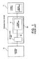
- Fig. 2 is a block diagram showing a structure of a conventional emulation device;
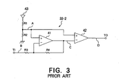
- Fig. 3 is a circuit diagram of an exemplified analog circuit provided in a peripheral evaluation chip illustrated in Fig. 2;
- Figs. 4A through 4D show a waveform chart for use in describing effects of noise generated in an analog circuit illustrated in Fig. 3;
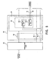
- Fig. 5 is a block diagram showing a structure of an emulation device according to a preferred embodiment of the present invention; and
- Figs. 6A through 6D show a waveform chart for use in describing operation of an analog circuit provided in a peripheral evaluation chip illustrated in Fig. 5.
-
- Referring to Figs. 1 through 4, a conventional emulation device is described for the purpose of facilitating the understanding of the present invention.
- In Fig. 1, an
emulation device 10 is used for an application system with a microcomputer that is to be designated as atarget system 11 to debug hardware and software of thetarget system 11 under the control of acontrol device 12. Theemulation device 10 comprises anemulation unit 20 and aprobe 30. Theprobe 30 is for use in connecting theemulation unit 20 to thetarget system 11. Theprobe 30 has aprobe connector 31 and acable assembly 32 for use in connecting theemulation unit 20 with theprobe connector 31. In other words, theprobe connector 31 is provided at an end of thecable assembly 32. Theprobe connector 31 has an integrated circuit for use in emulating peripheral functions of the microcomputer in thetarget system 11. This integrated circuit is referred hereinafter as a peripheral evaluation chip. - In Fig. 2, the
emulation unit 20 carries out operations of a central processing unit (CPU) of the microcomputer in thetarget system 11 and complementary operations for debugging hardware and software of thetarget system 11. Thecable assembly 32 is an assembly of lines including a power supply line 32-1 and a ground line 32-2. The power supply line 32-1 and the ground line 32-2 are each connected to thetarget system 11 and supply electric power to aperipheral evaluation chip 33 that is mounted on theprobe connector 31. - The
peripheral evaluation chip 33 on theprobe connector 31 is an integrated circuit adapted to emulate peripheral functions of the microcomputer in thetarget system 11. Theperipheral evaluation chip 33 is provided with the power from both theemulation unit 20 and thetarget system 11 via the power supply line 32-1. The ground line 32-2 is used to connect theemulation unit 20 with thetarget system 11. Thisperipheral evaluation chip 33 typically contains a digital circuit 33-1 and an analog circuit 33-2. - The
emulation unit 20 comprises a plurality of integrated circuits (ICs) such as large-scale integrated circuits (LSIs). Theemulation unit 20 is thus affected by instantaneous change in an internal signal in ICs as well as by the impedance of the power supply line 32-1 and the ground line 32-2. As a result, power supply noise is generated on the power supply line 32-1 and the ground line 32-2. In addition, thecable assembly 32 may serve as an antenna because it is relatively long. This causes electro-magnetically induced noise on thecable assembly 32. Such power supply noise or electro-magnetically induced noise affects theperipheral evaluation chip 33 on theprobe connector 31 through thecable assembly 32. If it happens, the analog circuit 33-2 contained in theperipheral evaluation chip 33 may be operated in a wrong or false manner due to the power supply noise or the electro-magnetically induced noise. - Effects of the power supply noise or the electro-magnetically induced noise in the analog circuit 33-2 are described with reference to Figs. 3 and 4. In Fig. 3, the analog circuit 33-2 comprises an
operational amplifier 41, acomparator 42, resistors R1 and R2 for dividing voltage, a resistor R3 for signal input, and a feedback resistor R4. Power is supplied to the analog circuit 33-2 from apower supply 43 through the resistor R1. The analog circuit 33-2 reverse-amplifies at the operational amplifier an analog micro-signal received by an input terminal TI. An output of theoperational amplifier 41 is converted into a digital signal by thecomparator 42 and is produced through an output terminal T0. - A reference voltage VREF is generated by dividing the voltage of the
power supply 43 by the use of the resistors R1 and R2. This reference voltage VREF is applied to a point A at positive input terminals of theoperational amplifier 41 and thecomparator 42. As shown in Fig. 4A, unstable, small waves are added to the reference voltage VREF due to the power supply noise or the electro-magnetically induced noise. - It is assumed that the input signal indicated in Fig. 4B is supplied to a point B on the input terminal TI. In such a case, the input signal is supplied to a negative input terminal of the
operational amplifier 41 through the resistor R3 and is reverse-amplified by theoperational amplifier 41. However, the reverse-amplified signal exhibits a waveform of the amplified signal with unstable, small waves added thereto as shown in Fig. 4C. The reference signal VREF indicated in Fig. 4A is responsible for it. The output of theoperational amplifier 41 is supplied to the negative input terminal of thecomparator 42. As a result, the digital output signal obtained over a point D on the output terminal T0 of thecomparator 42 has bread-shaped pulses with small waves at the edge of the waveform of the pulse, as shown in Fig. 4D. The bread-shaped pulses would cause faulty operation of the emulation device. - Two conventional approaches to the above mentioned problems are described. A first one is to prevent the aforementioned power supply noise from entering the analog circuit 33-2 in the
peripheral evaluation chip 33. In other words, this approach lies in avoiding generation of any power supply noise in the emulation device unit. - This first approach lowers the impedance across the power supply and the ground by means of increasing the thickness of wiring patterns of the power supply and the ground printed on a printed wiring board on which the ICs in the emulation unit are mounted. It is thus necessary to further increase the thickness of the wiring patterns of the power supply and the ground when highfrequency noise should be removed. This in turn requires increasing the size of the printed wiring board. To increase the size of the printed wiring board requires extra costs. In addition, there is a limitation on the size of the printed wiring board.
- A second approach uses a bypass capacitor. More specifically, a capacitor is connected between the power supply line and the ground line of the analog circuit 33-2 in the
peripheral evaluation chip 33. This second approach can be realized easily but the type of the capacitor used is the limitation on the frequency of the power supply noise that the capacitor can remove. - Referring to Figs. 5 and 6, an emulation device according to a preferred embodiment of the present invention is described. The emulation device according to the present invention is connected between the
control device 12 and thetarget system 11 as described in conjunction with Fig. 1. A feature of the emulation device according to the present invention lies in the connection between the analog circuit 33-2 in theperipheral evaluation chip 33 on a probe 30' with the power supply line and the ground line. More specifically, the analog circuit 33-2 is connected to thetarget system 11 via apower supply line 51 and aground line 52 to receive power from thetarget system 11. Thepower supply line 51 and theground line 52 are independent of the power supply line 32-1 and the ground line 32-2, respectively, described in conjunction with Fig. 2. - The
emulation unit 20 is controlled by thecontrol device 12 and serves as a CPU of the microcomputer in thetarget system 11 to be emulated. Theemulation unit 20 thus operates thetarget system 11. - As described above, the probe 30' connects the
emulation unit 20 and thetarget system 11. the probe 30' comprises theprobe connector 31 and thecable assembly 32. Thecable assembly 32 is a set of lines including the power supply line 32-1 and the ground line 32-2. Theprobe connector 31 is provided with theperipheral evaluation chip 33 mounted thereon. Theperipheral evaluation chip 33 is an integrated circuit that is used to emulate peripheral functions of the microcomputer in thetarget system 11. Theperipheral evaluation chip 33 comprises the digital circuit 33-1 and the analog circuit 33-2. - The power supply line and the ground line for the digital circuit 33-1 and the analog circuit 33-2 in the
peripheral evaluation chip 33 are different from those in the conventional peripheral evaluation chip. The power supply lines and the ground lines of this invention are independent of each other in theperipheral evaluation chip 33. The digital circuit 33-1 is connected to both theemulation unit 20 and thetarget system 11 through the power supply line 32-1 and the ground line 32-2. The analog circuit 33-2 is connected to thetarget system 11 through thepower supply line 51 and theground line 52, that are independent of the power supply line 32-1 and the ground line 32-2, respectively. - The
power supply line 51 and theground line 52 connected to the analog circuit 33-2 are short unlike thelong cable assembly 32 in the probe 30'. Therefore, no electro-magnetically induced noise is generated. In addition, the circuit in thetarget system 11 is significantly smaller in size than the circuit in theemulation unit 20, so that the power supply noise is hardly generated. This means that the analog circuit 33-2 is not affected by the power supply noise, avoiding the faulty operation of the emulation device which otherwise may be caused due to the power supply noise. - In Fig. 6, the analog circuit 33-2 illustrated in Fig. 3 operates as follows with the emulation device according to the present invention.
- The reference voltage VREF is generated by dividing the voltage of the
power supply 43 by the use of the resistors R1 and R2. This reference voltage VREF is applied to the point A at positive input terminals of theoperational amplifier 41 and thecomparator 42. The reference voltage VREF has a constant value as shown in Fig. 6A because no electro-magnetically induced noise exists. It is assumed that the input signal indicated in Fig. 6B is supplied to the point B on the input terminal TI. In such a case, the input signal is supplied to a negative input terminal of theoperational amplifier 41 through the resistor R3 and is reverse-amplified by theoperational amplifier 41. The reverse-amplified signal exhibits a stable waveform as shown in Fig. 6C because the reference signal VREF is stable. The output of theoperational amplifier 41 is supplied to the negative input terminal of thecomparator 42. As a result, the digital output signal obtained over the point D on the output terminal T0 of thecomparator 42 has a precise pulsed waveform, as shown in Fig. 6D. The analog circuit 33-2 in theperipheral evaluation chip 33 can operate without any faulty operation. - The above mentioned description has thus been made in conjunction with the case where the analog circuit 33-2 in the
peripheral evaluation chip 33 is connected to thetarget system 11 via the shortpower supply line 51 and theground line 52. However, thepower supply line 51 and theground line 52 may be connected to another system such as an independent power supply system rather than thetarget system 11. In addition, while the description has been made as theemulation unit 20 emulates the CPU of the microcomputer in thetarget system 11, the identical effect can be made when it is emulated by the peripheral evaluation chip mounted on theprobe connector 31 of the peripheral evaluation device.
Claims (2)
- An emulation device comprising an emulation unit (20) having a debugging function and a probe (30') for use in connecting the emulation unit with a target system, said probe comprising a cable assembly (32) for use in connecting said target system to said emulation unit and a probe connector (33) including an analog circuit (33-2) to emulate at least a part of functions of said target system, which is characterized in that
a power supply and a ground for said analog circuit being connected to said target system via a first power supply line (51) and a first ground line (52), respectively, that are independent of said cable assembly and that are short in length relative to said cable assembly. - An emulation device as claimed in Claim 1, wherein
said probe connector further comprises a digital circuit (33-1) to emulate at least a part of functions of said target system, a power supply and a ground of said digital circuit being connected to a second power supply line (32-1) and a second ground line (32-2), respectively, that are contained in said cable assembly.
Applications Claiming Priority (3)
| Application Number | Priority Date | Filing Date | Title |
|---|---|---|---|
| JP179181/96 | 1996-07-09 | ||
| JP17918196 | 1996-07-09 | ||
| JP8179181A JP3026299B2 (en) | 1996-07-09 | 1996-07-09 | Emulation device |
Publications (2)
| Publication Number | Publication Date |
|---|---|
| EP0820009A1 EP0820009A1 (en) | 1998-01-21 |
| EP0820009B1 true EP0820009B1 (en) | 2002-01-30 |
Family
ID=16061362
Family Applications (1)
| Application Number | Title | Priority Date | Filing Date |
|---|---|---|---|
| EP97111458A Expired - Lifetime EP0820009B1 (en) | 1996-07-09 | 1997-07-07 | Emulation device with no fear of faulty operation due to noise |
Country Status (5)
| Country | Link |
|---|---|
| US (1) | US6009260A (en) |
| EP (1) | EP0820009B1 (en) |
| JP (1) | JP3026299B2 (en) |
| KR (2) | KR100291728B1 (en) |
| DE (1) | DE69710132T2 (en) |
Families Citing this family (5)
| Publication number | Priority date | Publication date | Assignee | Title |
|---|---|---|---|---|
| WO2001001245A1 (en) * | 1999-06-26 | 2001-01-04 | Yang Sei Yang | Input/output probing apparatus and input/output probing method using the same, and mixed emulation/simulation method based on it |
| US6947883B1 (en) * | 2000-07-19 | 2005-09-20 | Vikram Gupta | Method for designing mixed signal integrated circuits and configurable synchronous digital noise emulator circuit |
| KR20030042747A (en) * | 2001-11-23 | 2003-06-02 | 주식회사 씨피씨 | Multi in-line drive type press apparatus |
| JP2008077176A (en) * | 2006-09-19 | 2008-04-03 | Seiko Epson Corp | Emulation system and emulation method |
| KR101113198B1 (en) | 2010-10-27 | 2012-02-15 | (주)탑에이테크놀로지 | Clamps for Multiclip Magazine and Multiclip Magazine |
Family Cites Families (15)
| Publication number | Priority date | Publication date | Assignee | Title |
|---|---|---|---|---|
| JPH029937A (en) * | 1988-06-27 | 1990-01-12 | Daihatsu Motor Co Ltd | Failure diagnosis for exhaust circulation control device |
| US5581695A (en) * | 1990-05-09 | 1996-12-03 | Applied Microsystems Corporation | Source-level run-time software code debugging instrument |
| US5056033A (en) * | 1990-07-24 | 1991-10-08 | Hewlett-Packard Company | Microprocessor emulator active probe power supply |
| JPH04128940A (en) * | 1990-09-20 | 1992-04-30 | Nec Ic Microcomput Syst Ltd | Emulator |
| US5375228A (en) * | 1991-02-04 | 1994-12-20 | Analog Devices, Inc. | Real-time signal analysis apparatus and method for digital signal processor emulation |
| JPH05257731A (en) * | 1992-03-11 | 1993-10-08 | Nec Corp | Probe terminating device for incircuit emulator |
| JPH05313936A (en) * | 1992-05-08 | 1993-11-26 | Nec Corp | In-circuit emulator |
| US5383137A (en) * | 1992-12-03 | 1995-01-17 | Motorola, Inc. | Emulation system and method for development of a low power data processor |
| JPH0728665A (en) * | 1993-07-07 | 1995-01-31 | Nec Corp | Emulation device for microcomputer |
| US5539901A (en) * | 1993-09-30 | 1996-07-23 | Intel Corporation | Method and apparatus for system management mode support for in-circuit emulators |
| JPH08147185A (en) * | 1994-11-22 | 1996-06-07 | Hitachi Ltd | emulator |
| US5630102A (en) * | 1994-12-19 | 1997-05-13 | Intel Corporation | In-circuit-emulation event management system |
| JP3380827B2 (en) * | 1995-02-09 | 2003-02-24 | 三菱電機株式会社 | Emulator device |
| JPH08278900A (en) * | 1995-04-04 | 1996-10-22 | Mitsubishi Electric Corp | Emulator probe |
| US5717699A (en) * | 1996-07-18 | 1998-02-10 | Hewlett-Packard Company | Method and apparatus for accessing internal integrated circuit signals |
-
1996
- 1996-07-09 JP JP8179181A patent/JP3026299B2/en not_active Expired - Fee Related
-
1997
- 1997-07-07 EP EP97111458A patent/EP0820009B1/en not_active Expired - Lifetime
- 1997-07-07 DE DE69710132T patent/DE69710132T2/en not_active Expired - Fee Related
- 1997-07-08 KR KR1019970031461A patent/KR100291728B1/en not_active Expired - Fee Related
- 1997-07-09 US US08/890,051 patent/US6009260A/en not_active Expired - Fee Related
-
1998
- 1998-02-12 KR KR1019980004109A patent/KR100241633B1/en not_active Expired - Lifetime
Also Published As
| Publication number | Publication date |
|---|---|
| KR980008525A (en) | 1998-04-30 |
| KR100241633B1 (en) | 2000-03-02 |
| JP3026299B2 (en) | 2000-03-27 |
| DE69710132T2 (en) | 2002-09-05 |
| KR980010775A (en) | 1998-04-30 |
| US6009260A (en) | 1999-12-28 |
| EP0820009A1 (en) | 1998-01-21 |
| JPH1027112A (en) | 1998-01-27 |
| DE69710132D1 (en) | 2002-03-14 |
| KR100291728B1 (en) | 2001-07-12 |
Similar Documents
| Publication | Publication Date | Title |
|---|---|---|
| EP0371696A3 (en) | Electronic system having a microprocessor and a coprocessor disposed on a circuit mounting board | |
| US6009260A (en) | Emulation device with no fear of faulty operation due to noise | |
| JPH0213985Y2 (en) | ||
| KR100216648B1 (en) | Interface circuit | |
| JPS61193220A (en) | Initialization circuit for output signal | |
| JPH0438303Y2 (en) | ||
| JPH04243329A (en) | Crosstalk reduction transmission circuit | |
| JPH07302143A (en) | Termination control circuit | |
| US5596470A (en) | Fault current protection circuit for an auxiliary device in a digital telephone system | |
| JPS633171Y2 (en) | ||
| JPH0628073A (en) | Terminal resistor circuit | |
| JP2708497B2 (en) | Misplacement detection device for electrical components | |
| JPH01219918A (en) | Electronic apparatus | |
| KR100256316B1 (en) | A self-tesing apparatus of washing machine | |
| KR0176206B1 (en) | Short prevention and noise reduction device of target board of application development device | |
| JPH0578941B2 (en) | ||
| JPS6237492B2 (en) | ||
| JPH0353603A (en) | Input buffer circuit | |
| JPS62224835A (en) | Adapter for connecting microcomputer | |
| KR200159809Y1 (en) | Warming up circuit for power stabilizing circuit | |
| JPH06149429A (en) | Pull-up resistor switching circuit | |
| JPH04128940A (en) | Emulator | |
| JPS5665503A (en) | Address code setting circuit | |
| JPS63200262A (en) | Microprocessor | |
| JPS6326024A (en) | Connector |
Legal Events
| Date | Code | Title | Description |
|---|---|---|---|
| PUAI | Public reference made under article 153(3) epc to a published international application that has entered the european phase |
Free format text: ORIGINAL CODE: 0009012 |
|
| AK | Designated contracting states |
Kind code of ref document: A1 Designated state(s): DE FR GB |
|
| AX | Request for extension of the european patent |
Free format text: AL;LT;LV;RO;SI |
|
| 17P | Request for examination filed |
Effective date: 19980520 |
|
| AKX | Designation fees paid |
Free format text: DE FR GB |
|
| RBV | Designated contracting states (corrected) |
Designated state(s): DE FR GB |
|
| 17Q | First examination report despatched |
Effective date: 20000704 |
|
| GRAG | Despatch of communication of intention to grant |
Free format text: ORIGINAL CODE: EPIDOS AGRA |
|
| GRAG | Despatch of communication of intention to grant |
Free format text: ORIGINAL CODE: EPIDOS AGRA |
|
| GRAH | Despatch of communication of intention to grant a patent |
Free format text: ORIGINAL CODE: EPIDOS IGRA |
|
| GRAH | Despatch of communication of intention to grant a patent |
Free format text: ORIGINAL CODE: EPIDOS IGRA |
|
| GRAA | (expected) grant |
Free format text: ORIGINAL CODE: 0009210 |
|
| REG | Reference to a national code |
Ref country code: GB Ref legal event code: IF02 |
|
| AK | Designated contracting states |
Kind code of ref document: B1 Designated state(s): DE FR GB |
|
| PG25 | Lapsed in a contracting state [announced via postgrant information from national office to epo] |
Ref country code: FR Free format text: LAPSE BECAUSE OF FAILURE TO SUBMIT A TRANSLATION OF THE DESCRIPTION OR TO PAY THE FEE WITHIN THE PRESCRIBED TIME-LIMIT Effective date: 20020130 |
|
| REF | Corresponds to: |
Ref document number: 69710132 Country of ref document: DE Date of ref document: 20020314 |
|
| PG25 | Lapsed in a contracting state [announced via postgrant information from national office to epo] |
Ref country code: GB Free format text: LAPSE BECAUSE OF NON-PAYMENT OF DUE FEES Effective date: 20020707 |
|
| EN | Fr: translation not filed | ||
| PLBE | No opposition filed within time limit |
Free format text: ORIGINAL CODE: 0009261 |
|
| STAA | Information on the status of an ep patent application or granted ep patent |
Free format text: STATUS: NO OPPOSITION FILED WITHIN TIME LIMIT |
|
| 26N | No opposition filed | ||
| GBPC | Gb: european patent ceased through non-payment of renewal fee |
Effective date: 20020707 |
|
| PGFP | Annual fee paid to national office [announced via postgrant information from national office to epo] |
Ref country code: DE Payment date: 20040715 Year of fee payment: 8 |
|
| PG25 | Lapsed in a contracting state [announced via postgrant information from national office to epo] |
Ref country code: DE Free format text: LAPSE BECAUSE OF NON-PAYMENT OF DUE FEES Effective date: 20060201 |