EP0820061A2 - Appareil de lecture et méthode de lecture - Google Patents
Appareil de lecture et méthode de lecture Download PDFInfo
- Publication number
- EP0820061A2 EP0820061A2 EP97112036A EP97112036A EP0820061A2 EP 0820061 A2 EP0820061 A2 EP 0820061A2 EP 97112036 A EP97112036 A EP 97112036A EP 97112036 A EP97112036 A EP 97112036A EP 0820061 A2 EP0820061 A2 EP 0820061A2
- Authority
- EP
- European Patent Office
- Prior art keywords
- signal
- value
- interpolation
- phase
- circuit
- Prior art date
- Legal status (The legal status is an assumption and is not a legal conclusion. Google has not performed a legal analysis and makes no representation as to the accuracy of the status listed.)
- Withdrawn
Links
Images


Classifications
-
- H—ELECTRICITY
- H03—ELECTRONIC CIRCUITRY
- H03L—AUTOMATIC CONTROL, STARTING, SYNCHRONISATION OR STABILISATION OF GENERATORS OF ELECTRONIC OSCILLATIONS OR PULSES
- H03L7/00—Automatic control of frequency or phase; Synchronisation
- H03L7/06—Automatic control of frequency or phase; Synchronisation using a reference signal applied to a frequency- or phase-locked loop
- H03L7/08—Details of the phase-locked loop
-
- G—PHYSICS
- G11—INFORMATION STORAGE
- G11B—INFORMATION STORAGE BASED ON RELATIVE MOVEMENT BETWEEN RECORD CARRIER AND TRANSDUCER
- G11B20/00—Signal processing not specific to the method of recording or reproducing; Circuits therefor
- G11B20/10—Digital recording or reproducing
- G11B20/10009—Improvement or modification of read or write signals
- G11B20/10037—A/D conversion, D/A conversion, sampling, slicing and digital quantisation or adjusting parameters thereof
-
- G—PHYSICS
- G11—INFORMATION STORAGE
- G11B—INFORMATION STORAGE BASED ON RELATIVE MOVEMENT BETWEEN RECORD CARRIER AND TRANSDUCER
- G11B20/00—Signal processing not specific to the method of recording or reproducing; Circuits therefor
- G11B20/10—Digital recording or reproducing
- G11B20/14—Digital recording or reproducing using self-clocking codes
- G11B20/1403—Digital recording or reproducing using self-clocking codes characterised by the use of two levels
-
- G—PHYSICS
- G11—INFORMATION STORAGE
- G11B—INFORMATION STORAGE BASED ON RELATIVE MOVEMENT BETWEEN RECORD CARRIER AND TRANSDUCER
- G11B20/00—Signal processing not specific to the method of recording or reproducing; Circuits therefor
- G11B20/10—Digital recording or reproducing
- G11B20/18—Error detection or correction; Testing, e.g. of drop-outs
- G11B20/1876—Interpolating methods
-
- H—ELECTRICITY
- H03—ELECTRONIC CIRCUITRY
- H03L—AUTOMATIC CONTROL, STARTING, SYNCHRONISATION OR STABILISATION OF GENERATORS OF ELECTRONIC OSCILLATIONS OR PULSES
- H03L7/00—Automatic control of frequency or phase; Synchronisation
- H03L7/06—Automatic control of frequency or phase; Synchronisation using a reference signal applied to a frequency- or phase-locked loop
- H03L7/08—Details of the phase-locked loop
- H03L7/085—Details of the phase-locked loop concerning mainly the frequency- or phase-detection arrangement including the filtering or amplification of its output signal
- H03L7/091—Details of the phase-locked loop concerning mainly the frequency- or phase-detection arrangement including the filtering or amplification of its output signal the phase or frequency detector using a sampling device
-
- H—ELECTRICITY
- H03—ELECTRONIC CIRCUITRY
- H03L—AUTOMATIC CONTROL, STARTING, SYNCHRONISATION OR STABILISATION OF GENERATORS OF ELECTRONIC OSCILLATIONS OR PULSES
- H03L7/00—Automatic control of frequency or phase; Synchronisation
- H03L7/06—Automatic control of frequency or phase; Synchronisation using a reference signal applied to a frequency- or phase-locked loop
- H03L7/08—Details of the phase-locked loop
- H03L7/099—Details of the phase-locked loop concerning mainly the controlled oscillator of the loop
- H03L7/0991—Details of the phase-locked loop concerning mainly the controlled oscillator of the loop the oscillator being a digital oscillator, e.g. composed of a fixed oscillator followed by a variable frequency divider
- H03L7/0994—Details of the phase-locked loop concerning mainly the controlled oscillator of the loop the oscillator being a digital oscillator, e.g. composed of a fixed oscillator followed by a variable frequency divider comprising an accumulator
Definitions
- the present invention relates to a playback apparatus and a playback method.
- the invention relates to a playback apparatus and a playback method for generating a second clock signal in synchronization with a first clock signal by adjusting the clock frequency of the second clock signal in accordance with a phase error of an interpolation value and for computing the interpolation value at a predetermined phase of the second clock signal from values obtained as a result of sampling a predetermined signal (including the first clock signal) in synchronization with the first clock signal.
- a compact disk a representative recording medium for storing digital data, is becoming more and more popular in a wide range of applications.
- a clock signal is extracted from a signal detected from the disk and digital data is then reproduced from the detected signal in synchronization with the extracted clock signal. Synchronization of extracting data from a signal with a clock signal extracted from the same signal is referred to as the so-called self synchronization.
- the clock signal is extracted from the detected signal by using a PLL (Phase Locked Loop) circuit.
- PLL Phase Locked Loop
- Fig. 1 is a diagram showing a typical configuration of the related art playback apparatus having an analog PLL circuit.
- a read-out device 101 radiates a laser beam to an optical disk 111 such as a compact disk and receives a laser beam reflected by the optical disk 111, that is, a return light coming from the optical disk 111.
- An electrical signal representing the quantity of the incoming return light is then supplied by the read-out device 101 to a waveform shaping unit 102.
- the electrical signal is the so-called playback signal.
- the waveform shaping unit 102 converts the playback signal supplied by the read-out device 101 into a binary signal and outputs the binary signal to a latch circuit 103 and an analog PLL circuit 104 as a playback signal.
- the analog PLL circuit 104 extracts a clock signal from the playback signal supplied by the waveform shaping unit 102 and supplies the clock signal to the latch circuit 103. Values of the binary playback signal which are either 0 or 1 change at intervals each equal to a multiple of a predetermined bit period T. It should be noted that the intervals each correspond to a piece of data recorded on the optical disk 111.
- the analog PLL circuit 104 extracts the bit period T from the interval, generating a clock signal having a period corresponding to the bit period T.
- a phase comparator 121 computes a phase error between the playback signal supplied by the waveform shaping unit 102 and a clock signal (a PLL clock signal) oscillated by a voltage controlled oscillator (VCO) 123.
- the phase error is output by the phase comparator 121 to a loop filter 122 for eliminating high frequency components, that is, components in an unnecessary frequency band, from the phase error.
- the loop filter 122 outputs the processed phase error to the VCO 123.
- the VCO 123 oscillates the PLL clock signal while adjusting the frequency thereof so that the phase error with respect to the playback signal supplied by the waveform shaping unit 102 is eliminated.
- the PLL clock signal is fed back to the phase comparator 121 and supplied to the latch circuit 103.
- the analog PLL circuit 104 generates the PLL clock signal synchronized with the playback signal.
- the latch circuit 103 outputs the playback signal supplied by the waveform shaping circuit 102 in synchronization with the PLL clock signal oscillated by the analog PLL circuit 104 to a playback circuit at the following stage which is not shown in the figure.
- the analog PLL circuit 104 has a problem that it is easily affected by changes in environment, changes with the lapse of time and component variations. There is also raised a problem that it is difficult to put the analog PLL circuit in a highly integrated circuit chip due to the fact that the PLL circuit is an analog circuit.
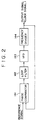
- Fig. 2 is a diagram showing a typical configuration of a digital PLL circuit.
- the digital PLL circuit comprises a digital phase comparator 141, a digital loop filter 142 and a variable frequency oscillator (VFO) 143 as a substitute for the VCO.
- the VFO 143 adjusts the frequency of an output signal thereof by adding or eliminating pulses to and from the output signal in accordance with the digital value of a phase error supplied by the digital phase comparator 141 to the VFO 143 by way of the digital loop filter 142.
- the VFO 143 adjusts the frequency of an output signal thereof by switching the generation of the output signal from one embedded oscillator to the other embedded one in accordance with the digital value of a phase error supplied by the digital phase comparator 141 to the VFO 143 by way of the digital loop filter 142.
- the VFO 143 In order to adjust the oscillation frequency smoothly in accordance with phase error, the VFO 143 generates an interim output signal with a frequency equal to a multiple of the frequency of a finally desired clock signal by adjusting the frequency of the interim output signal.
- the VFO 143 supplies the interim output signal to a frequency divider 144 for dividing the frequency thereof.
- the output of the frequency divider 144 is the finally desired clock signal which is fed back to the digital phase comparator 141 and supplied to a circuit at the following stage which is not shown in the figure.
- the analog playback signal is converted by an A/D (analog to digital) converter into digital data which is then supplied a so-called computer for carrying out virtual PLL processing by software.
- A/D analog to digital
- the speed of the software PLL processing is low, making it difficult to apply such a computer-based VFO to an apparatus that requires a high processing speed.
- the present invention addresses the problems described above. It is thus an object of the present invention to provide a playback apparatus capable of self-synchronizing a playback signal (including a first clock signal) by means of digital circuits for generating a second clock signal in synchronization with the first clock signal by adjusting the clock frequency of the second clock signal in accordance with a phase error of an interpolation value and for computing the interpolation value at a predetermined phase of the second clock signal from values obtained as a result of sampling the playback signal in synchronization with the first clock signal.
- the present invention provides a playback apparatus characterized by comprising an interpolation value computing unit for computing an interpolation value at a third point of time corresponding to a predetermined phase of a second clock signal from two values obtained by consecutively sampling a predetermined signal at a first point of time and a second point of time by linear interpolation.
- the present invention also provides a playback method characterized by comprising the step of computing an interpolation value at a third point of time corresponding to a predetermined phase of a second clock signal from two values obtained by consecutively sampling a predetermined signal at a first point of time and a second point of time by linear interpolation based on a relation between the first, second and third points of time.
- the present invention also provides a playback apparatus characterized by comprising a clock signal generating unit for computing a sum of a value of a second clock signal computed previously and a first constant and then:
- the present invention also provides a playback method characterized by comprising the steps of:
- the interpolation value computing unit computes an interpolation value at a third point of time corresponding to a predetermined phase of a second clock signal from two values obtained by consecutively sampling a predetermined signal at a first point of time and a second point of time by linear interpolation.
- the playback method includes the step of computing an interpolation value at a third point of time corresponding to a predetermined phase of a second clock signal from two values obtained by consecutively sampling a predetermined signal at a first point of time and a second point of time by linear interpolation based on a relation between the first, second and third points of time.
- the clock signal generating unit computes a sum of a value of a second clock signal computed previously and a first constant and then:
- the playback method includes the steps of:
- FIG. 3 is a diagram showing a typical configuration of an embodiment implementing a playback apparatus provided by the present invention.
- a read-out device 1 radiates a laser beam to an optical disk 111 such as a compact disk and receives a laser beam reflected by the optical disk 111, that is, a return light coming from the optical disk 111.
- An electrical signal representing the quantity of the incoming return light, that is, a playback signal, is then supplied by the read-out device 1 to an A/D converter 2.
- the A/D converter 2 supplies an interpolation circuit (or an interpolation value computing unit) 3 with sampled values, digital values each having a predetermined number of bits, which are obtained by sampling the playback signal coming from the read-out device 1 in synchronization with a system clock signal (which is also referred to as a first clock signal).
- a system clock signal which is also referred to as a first clock signal.
- the interpolation circuit 3 operates in accordance with the system clock signal.
- a PLL clock phase signal P (also referred to as a second clock signal) is supplied by a PLL clock phase signal generator (also referred to as a clock signal generator) 7 to the interpolation circuit 3 in synchronization with the system clock signal.
- a value (referred to as an interpolation value) of the playback signal at the time the phase of the PLL clock phase signal P becomes zero is computed from the sampled values supplied to the interpolation circuit 3 by the A/D converter 2 by using a linear interpolation technique.
- the interpolation value digital data with a predetermined number of bits, is then supplied to a binary conversion circuit 4 and fed back to a phase error detecting circuit (also referred to as a phase error computing unit) 5.
- the binary conversion circuit 4 converts the interpolation value of the playback signal supplied thereto by the interpolation circuit 3 into a binary value, that is, into 0 or 1. The binary value is then supplied to a circuit at the following stage which is not shown in the figure.
- the phase error detecting circuit 5 detects a transition of the interpolation value of the playback signal supplied thereto by the interpolation circuit 3 from positive to negative or vice versa which is known as a zero cross. The zero cross timing is then used for generating a phase error signal which is then output to a loop filter 6.
- the loop filter 6 passes on the phase error signal supplied by the phase error detecting circuit 5 to the PLL clock phase signal generator 7 after removing high frequency components from the phase error signal.
- the PLL clock phase signal generator 7 generates the PLL clock phase signal P having a saw-tooth waveform (with the frequency thereof) determined by the phase error signal which is supplied by the loop filter 6 with the high frequency components thereof removed.
- the PLL clock phase signal P is supplied to the interpolation circuit 3 as described above.
- Fig. 4 is a diagram showing a typical configuration of the interpolation circuit 3.
- the interpolation circuit 3 includes a delay device 21 for holding a sampled value S i resulting from sampling by the A/D converter 2 at a time t i till the next system clock and outputting the sampled value S i at the next clock to a multiplier 22.
- the multiplier 22 computes the product (S i -1 X P i ) of a sampled value S i-1 at a time t i-1 supplied thereto by the delay device 21 and a value P i of the PLL clock phase signal P supplied by the PLL clock phase signal generator 7, outputting the product (S i-1 X P i ) to an adder 23.
- the time t i-1 is a time earlier than the time t i by one system clock.
- An adder (used as a subtractor) 24 computes the difference (A - P i ) between the value P i of the PLL clock phase signal P supplied thereto by the PLL clock phase signal generator 7 and a constant A (also referred to as a first constant to be described later), outputting the difference (A - P i ) to a multiplier 25.
- the multiplier 25 computes the product (S i X (A - P i )) of the sampled value S i resulting from sampling by the A/D converter 2 at the time t i and the difference (A - P i ) supplied thereto by the adder 24, outputting the product (S i X (A - P i )) to the adder 23.
- the adder 23 computes the sum (S i-1 X P i + S i X (A - P i )) of the product (S i-1 X P i ) supplied thereto by the multiplier 22 and the product (S i X (A - P i )) supplied by the multiplier 25, outputting the sum (S i-1 X P i + S i X (A - P i )) to a latch circuit 26.
- a delay device 27 is used for holding a value P i of the PLL clock phase signal P generated by the PLL clock phase signal generator 7 at the time t i till the next system clock and outputting the value P i at the next clock to the phase zero cross detecting circuit 28.
- the phase zero cross detecting circuit 28 computes the difference (P i - P i-1 ) between the value P i-1 of the PLL clock phase signal P at the time t i-1 supplied thereto by the delay device 27 and the value P i of the PLL clock phase signal P at the time t i supplied by the PLL clock phase signal generator 7, finding out whether the difference (P i - P i-1 ) is positive or negative.
- the phase zero cross detecting circuit 28 forms a judgment that a phase zero cross has occurred in the PLL clock phase signal P, that is, the phase of the PLL clock phase signal P once became zero at a point of time between the times t i-1 and t i .
- the enable signal is output to the multipliers 22 and 25 as well as the latch circuit 26.
- the latch circuit 26 includes an embedded storage device. Receiving the enable signal from the phase zero cross detecting circuit 28, the latch circuit 26 updates a value stored in the storage device with a value supplied thereto from the adder 23 and, at the same time, outputs the value stored in the storage device to the binary conversion circuit 4 and feeds back the value to the phase error detecting circuit 5 as an interpolation value L i .
- Fig. 5 is a diagram showing a typical configuration of the phase error detecting circuit 5.
- the phase error detecting circuit 5 includes a delay device 41 for holding the interpolation value L i supplied by the interpolation circuit 3 for the period of a system clock and outputting the interpolation value L i at the next clock to a phase error computing circuit 42 and an interpolation value zero cross detecting circuit 43.
- the interpolation value zero cross detecting circuit 43 forms a judgment as to whether or not a zero cross has occurred in the interpolation value of the playback signal from an interpolation value L i-1 of the immediately preceding system clock supplied thereto by the delay device 41 and the interpolation value L i supplied by the interpolation circuit 3.
- the interpolation value zero cross detecting circuit 43 finds out whether or not the interpolation value L i-1 is positive while the interpolation value L i is negative, or whether or not the interpolation value L i-1 is negative while the interpolation value L i is positive. If the interpolation value L i-1 is found positive while the interpolation value L i is found negative, the interpolation value zero cross detecting circuit 43 forms a judgment that an interpolation value zero cross has occurred on the falling edge of the interpolation value. In this case, a signal indicating such a falling edge zero cross is output to the phase error computing circuit 42.
- the interpolation value zero cross detecting circuit 43 forms a judgment that an interpolation value zero cross has occurred on the rising edge of the interpolation value. In this case, a signal indicating such a rising edge zero cross is output to the phase error computing circuit 42.
- the phase error computing circuit 42 computes a phase error signal from the interpolation value L i-1 of the immediately preceding system clock supplied thereto by the delay device 41 and the interpolation value L i supplied by the interpolation circuit 3, outputting the phase error signal to the loop filter 6.
- the phase error computing circuit 42 computes the sum (L i-1 + L i ) of the interpolation values L i-1 and L i and outputs the sum (L i-1 + L i ) to the loop filter 6 as a phase error signal.
- the phase error computing circuit 42 computes the sum (L i-1 + L i ) of the interpolation values L i-1 and L i and multiplies the sum (L i-1 + L i ) by -1 to give a product (-(L i-1 + L i )), outputting the product (-(L i-1 + L i )) to the loop filter 6 as a phase error signal.
- Fig. 6 is a diagram showing a typical configuration of the PLL clock phase signal generator 7.
- the PLL clock phase signal generator 7 includes a phase register upper limit computing circuit 61, which also operates according to the system clock signal, for computing an upper limit value X (also referred to as a second constant) of a value held in a PLL clock phase register 67 in accordance with the value of the phase error signal supplied thereto by way of the loop filter 6.
- the upper limit value X is then output to an adder (used as a subtractor) 62 and a comparator 63.
- a constant generating circuit 64 generates the constant A cited earlier to be supplied to an adder 65 and the interpolation circuit 3. As described before, the constant A is also referred to as a first constant.
- the adder 65 computes the sum (P i + A) of the constant A supplied thereto by the constant generating circuit 64 and the PLL clock phase signal P i supplied by the PLL clock phase register 67, outputting the sum (P i + A) to the adder 62, the comparator 63 and a switch circuit 66.
- the adder 62 computes the difference (P i + A - X) between the sum (P i + A) supplied thereto by the adder 65 and the upper limit value X supplied by the phase register upper limit computing circuit 61, outputting the difference (P i + A - X) to the switch circuit 66.
- the comparator 63 compares the sum (P i + A) supplied thereto by the adder 65 with the upper limit value X supplied by the phase register upper limit computing circuit 61 by computing the difference (P i + A - X) between them.
- the comparator 63 also finds out whether the computed difference (P i + A - X) is positive or negative. If the computed difference (P i + A - X) is found positive, that is, if (P i + A) > X, a first control signal is supplied to the switch circuit 66. If the computed difference (P i + A - X) is found equal to or smaller than zero, that is, if (P i + A) ⁇ X, on the other hand, a second control signal is supplied to the switch circuit 66.
- the switch circuit 66 receives the first control circuit indicating (P i + A) > X, the switch circuit 66 passes on the difference (P i + A - X) supplied thereto by the adder 62 to the PLL clock phase register 67. If the second control circuit indicating (P i + A) ⁇ X is received, on the other hand, the switch circuit 66 forwards the sum (P i + A) supplied by the adder 65 to the PLL clock phase register 67.
- the PLL clock phase register 67 stores the difference (P i + A- X) or the sum (P i + A) supplied thereto by the switch circuit 66 in a storage device embedded therein and outputs the value (P i + A- X) or (P i + A) to the adder 65 and the interpolation circuit 3 shown in Fig. 1 as a value P i of the PLL clock phase signal P.
- the PLL clock phase signal generator 7 operates in accordance with the system clock signal, adding the constant A to the value P i of the PLL clock phase signal P in every system clock. As the sum (P i + A) exceeds the upper limit value X, the upper limit value X is subtracted from the sum (P i + A) to result in the difference (P i + A - X).
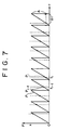
- the PLL clock phase signal generator 7 derives the value P i of the PLL clock phase signal P having a saw-tooth waveform with a maximum amplitude equal to X, the first constant, and a slope A/ ⁇ t where ⁇ t is the period of the system clock signal as shown in Fig. 7.
- the interpolation value zero cross detecting circuit 43 employed in the phase error detecting circuit 5 receives the interpolation value L i-1 of the playback signal for the immediately preceding system clock from the delay device 41 and the interpolation value L i for the present system clock from the interpolation circuit 3.
- the interpolation value zero cross detecting circuit 43 finds out whether or not the interpolation value L i-1 is negative while the interpolation value L i is positive. If the interpolation value L i-1 is found negative while the interpolation value L i is found positive, the interpolation value zero cross detecting circuit 43 forms a judgment that an interpolation value zero cross has occurred on the rising edge of the interpolation value. In this case, a signal indicating such a rising edge zero cross is output to the phase error computing circuit 42.
- the phase error computing circuit 42 computes the sum (L i -1 + L i ) of the interpolation value L i-1 of the immediately preceding system clock and the current interpolation value L i and outputs the sum (L i-1 + L i ) to the loop filter 6 as a phase error signal.
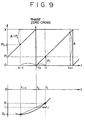
- Fig. 8A shows relations between the interpolation values L i-1 and L i at the time the rising edge zero cross is detected and the value of the phase error signal ⁇ . If the absolute value of the interpolation value L i is greater than the absolute value of the interpolation value L i-1 , the value of the phase error signal ⁇ is positive. If the absolute value of the interpolation value L i is smaller than the absolute value of the interpolation value L i-1 , on the other hand, the value of the phase error signal ⁇ is negative.
- the interpolation value zero cross detecting circuit 43 finds out whether or not the interpolation value L i-1 is positive while the interpolation value L i is negative. If the interpolation value L i-1 is found positive while the interpolation value L i is found negative, the interpolation value zero cross detecting circuit 43 forms a judgment that a interpolation value zero cross has occurred on the falling edge of the interpolation value. In this case, a signal indicating such a falling edge zero cross is output to the phase error computing circuit 42.
- the phase error computing circuit 42 computes the sum (L i -1 + L i ) of the interpolation value L i-1 of the immediately preceding system clock and the current interpolation value L i and multiplies the sum (L i-1 + L i ) by - 1 to give a product (-(L i-1 + L i )), outputting the product (- (L i-1 + L i )) to the loop filter 6 as a phase error signal.
- Fig. 8B shows relations between the interpolation values L i-1 and L i at the time the falling edge zero cross is detected and the value of the phase error signal ⁇ . If the absolute value of the interpolation value L i is greater than the absolute value of the interpolation value L i-1 , the value of the phase error signal ⁇ is positive. If the absolute value of the interpolation value L i is smaller than the absolute value of the interpolation value L i-1 , on the other hand, the value of the phase error signal ⁇ is negative.
- the interpolation value zero cross detecting circuit 43 does not output any signal to the phase error computing circuit 42 in particular.
- the phase error computing circuit 42 outputs a zero to the loop filter 6 as a phase error signal.
- an interpolation value L be obtained by applying a linear interpolation technique to the interpolation value L i-1 at the time t i-1 and the interpolation value L i at the time t i .
- the value L becomes zero at a time t 0 earlier or later than a middle point between the times t i-1 and t i .
- a positive phase error signal is supplied to the loop filter 6 be the interpolation value zero cross a rising edge zero cross or a falling edge zero cross.
- a negative phase error signal is supplied to the loop filter 6 regardless of whether the interpolation value zero cross is a rising edge interpolation value zero cross or a falling edge interpolation value zero cross.
- the PLL clock phase signal P generated by the PLL clock phase signal generator 7 is not supplied directly to the phase error detecting circuit 5. Instead, the PLL clock phase signal P generated by the PLL clockphase signal generator 7 is supplied indirectly to the phase error detecting circuit 5 by way of the interpolation circuit 3. It should be noted, however, that if a phase zero cross does not occur in the PLL clock phase signal, the interpolation value of the playback signal supplied from the interpolation circuit 3 to the phase error detecting circuit 5 is not updated by the interpolation circuit 3.
- the phase error detecting circuit 5 outputs a zero to the loop filter 6 as a phase error signal because the interpolation value L i and the interpolation value L i-1 , have the same sign as described above, indirectly reflecting the state of the PLL clock phase signal P in the operation thereof.
- the loop filter 6 outputs the phase error signal to the PLL clock phase signal generator 7 after eliminating high frequency components from the phase error signal.
- the loop filter 6 prevents a positive feedback with a much lagging phase in the high frequency zone in the PLL operation and, at the same time, reduces the number of intersymbol interference components and the amount of noise included in the playback signal.
- phase register upper limit computing circuit 61 employed in the PLL clock phase signal generator 7 computes an upper limit value X of a value held in the PLL clock phase register 67 in accordance with the value of the phase error signal supplied thereto by the phase error detecting circuit 5 by way of the loop filter 6.
- the upper limit value X is then output to the adder 62 (used as a subtractor) and the comparator 63.
- the comparator 63 compares the sum (P i + A) supplied thereto by the adder 65 with the upper limit value X supplied by the phase register upper limit computing circuit 61 by computing the difference (P i + A - X) between them. Then, the comparator 63 finds out whether the computed difference (P i + A - X) is positive or negative. If the computed difference (P i + A - X) is found positive, that is, if (P i + A) > X, a first control signal is supplied by the comparator 63 to the switch circuit 66. Receiving the first control circuit indicating (P i + A) > X, the switch circuit 66 passes on the difference (P i + A - X) supplied thereto by the adder 62 to the PLL clock phase register 67.
- the PLL clock phase register 67 stores the difference (P i + A - X) or the sum (P i + A) supplied thereto by the switch circuit 66 in a storage device embedded therein and outputs the value (P i + A - X) or (P i + A) to the interpolation circuit 3 as a value P i of the PLL clock phase signal P.
- the PLL clock phase signal generator 7 in each system clock derives the value P i of the PLL clock phase signal P having a saw-tooth waveform like the one shown in Fig. 7 and outputs the value P i to the interpolation circuit 3.
- the PLL clock phase signal generator 7 adjusts the frequency of the PLL clock phase signal P having a virtual saw-tooth waveform by adjusting the upper limit value X in accordance with the phase error signal.
- the interpolation circuit 3 detects a time (referred to as a third point of time) at which the phase of the virtual PLL clock phase signal P is zero from two consecutive values P i-1 and P i of the PLL clock phase signal P at the times t i-1 (referred to as a first point of time) and t i (referred to as a second point of time) respectively.
- a time referred to as a third point of time
- the phase of the PLL clock phase signal (strictly speaking, the value of the virtual PLL clock phase signal P) is zero, that is, a phase zero cross occurs.
- the value of the playback signal at the time the phase zero cross occurs is then calculated by the interpolation circuit 3 by using the linear interpolation technique from sampled values S i-1 and S i supplied thereto by the A/D converter 2.
- t z be the time at which a phase zero cross occurs in the virtual PLL clock phase signal P. Since the slope of the saw-tooth waveform of the PLL clock phase signal P is fixed as shown in Fig. 9, the ratio of (t i -t z ) to (t z - t i-1 ) is equal to the ratio of P i to (A - P i ) or ((t i - t z ) : (t z - t i-1 )) is equal to (P i : (A - P i )).
- the ratio of (t i - t z ) to (t z - t i-1 ) is equal to the ratio of (S i - L i ') to (L i ' - S i-1 ) or ((t i - t z ) : (t z - t i-1 )) is equal to ((S i - L i ') : (L i ' - S i-1 )).
- the ratio of (S i - L i ') to (L i ' - S i-1 ) is equal to the ratio of P i to (A - P i ) or ((S i - L i ') : (L i ' - S i-1 )) is equal to (P i : (A - P i )).
- the numerator (S i-1 X P i + S i X (A - P i )) of the ratio on the right hand side of the above equation is calculated by using the delay device 21, the multiplier 22, the adder 23, the adder 24 and the multiplier 25 employed in the interpolation circuit 3.
- the phase zero cross detecting circuit 28 computes the difference (P i - P i-1 ) between the value P i-1 of the PLL clock phase signal P at the time t i-1 , a point of time ahead of the present time t i by one system clock, supplied thereto by the delay device 27 and the value P i of the PLL clock phase signal P at the present time t i supplied by the PLL clock phase signal generator 7, finding out whether the difference (P i - P i-1 ) is positive or negative.
- the phase zero cross detecting circuit 28 forms a judgment that a phase zero cross has occurred in the PLL clock phase signal P, that is, the phase of the PLL clock phase signal P once became zero at a point of time between the times t -1 and t i .
- the enable signal is output to the multipliers 22 and 25 as well as the latch circuit 26.
- the multiplier 22 computes the product (S i-1 X P i ) of a sampled value S i-1 at a time t i-1 supplied thereto by the delay device 21 and a value P i of the PLL clock phase signal P supplied by the PLL clock phase signal generator 7, outputting the product (S i-1 X P i ) to the adder 23.
- the multiplier 25 computes the product (S i X (A - P i )) of a sampled value Si at a time t i supplied thereto by the A/D converter 2 and the difference (A - P i ) supplied by the adder 24, outputting the product (S i X (A - P i )) to the adder 23.
- the adder 23 computes the sum (S i-1 X P i + S i X (A - P i )) of the product (S i-1 X P i ) supplied thereto by the multiplier 22 and the product (S i X (A - P i )) supplied by the multiplier 25, outputting the sum (S i-1 X P i + S i X (A - P i )) to a latch circuit 26.
- the latch circuit 26 updates a value stored in the storage device with a value supplied thereto from the adder 23 and, at the same time, outputs the value stored in the storage device to the binary conversion circuit 4 and feeds back the value to the phase error detecting circuit 5 as an interpolation value L i .
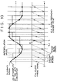
- Fig. 10 is a diagram showing an example of the interpolation value L i output by the latch circuit 26. If the difference (P i - P i-1 ) between the value P i-1 of the PLL clock phase signal P at the time t i-1 supplied by the delay device 27 and the value P i (denoted by an X mark) of the PLL clock phase signal P at the present time t i supplied by the PLL clock phase signal generator 7 indicates that a phase zero cross has occurred in the PLL clock phase signal P at a point of time between the times t i-1 and t i , the interpolation circuit 3 updates the interpolation value. If a phase zero cross did not occur in the PLL clock phase signal P at a point of time between the times t i-1 and t i , on the other hand, the interpolation circuit 3 does not update the interpolation value.
- the enable signal is not output to the multipliers 22 and 25 and the latch circuit 26.
- the latch circuit 26 outputs the interpolation value of the immediately preceding system clock as it is. Since the binary conversion circuit 4 carries out processing in synchronization with the enable signal generated by the phase zero cross detecting circuit 28, the interpolation value of the immediately preceding system clock output as it is by the latch circuit 26 is not processed by the binary conversion circuit 4 for the second time, that is, the same interpolation value of two consecutive system clocks is not processed twice.
- the phase error detecting circuit 5 detects a phase error, that is a deviation of a zero cross of the interpolation value occurring in the playback signal from a middle point of two consecutive system clocks.
- the PLL clock phase clock signal generator 7 uses the deviation to adjust the frequency of the virtual PLL clock phase signal P in order to adjust the timing for calculating an interpolation value, that is, the time at which the phase of the PLL clock phase signal P becomes zero. In this way, the interpolation value zero cross of the interpolation value occurring in the playback signal can be brought to a point of time closer to the middle point.
- the binary conversion circuit 4 can carry out binary conversion processing with a high degree accuracy even if the zero cross of the interpolation value occurring in the playback signal deviates from the middle point to a certain degree due to intersymbol interference and noise.
- all circuits composing the PLL such as the interpolation circuit 3 each operate in synchronization with the system clock signal.
- a circuit operating at a clock frequency higher than that of the system clock signal is not required even if high speed processing is to be carried out, allowing a low cost playback apparatus to be implemented.
- the present embodiment is obtained by modifying the interpolation circuit 3 and the PLL clock phase signal generator 7 employed in the previous embodiment described above. For this reason, only the interpolation circuit 3 and the PLL clock phase signal generator 7 are explained, omitting the description of the other components.
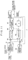
- Fig. 11 is a diagram showing a typical configuration of the PLL clock phase signal generator 7 employed in the present embodiment.
- the PLL clock phase signal generator 7 has a delay device 68 for holding the output of the comparator 63 for one period of the system clock signal before supplying the output to the interpolation circuit 3 and the binary conversion circuit 4 as an enable signal.
- the comparator 63 will detect the fact that the sum (P i + A) at the time t i is greater than the upper limit value X, thus, the output of the comparator 63 can be used as an enable signal of the previous embodiment described earlier.
- Fig. 12 is a diagram showing a typical configuration of the interpolation circuit 3 employed in the present embodiment.
- the enable signal generated by the PLL clock phase signal generator 7 is used, making it unnecessary to employ the delay device 27 and the phase zero cross detecting circuit 28 in the present interpolation circuit 3.
- the delay device 68 is employed in the PLL clock phase signal generator 7, it is not necessary to provide the delay device 27 and phase zero cross detecting circuit 28 in the present interpolation circuit 3. As a result, the number of components required by the playback apparatus implemented by the present embodiment can be reduced, allowing the circuit to be made simpler.
- the phase error detecting circuit 5 employed in the embodiments calculates a phase error from interpolation values, which are each obtained by using a linear interpolation technique, at a time of the occurrence of a zero cross of the interpolation values. It should be noted, however, that interpolation values obtained by using a high order interpolation technique can also be used for computing a phase error at a time of the occurrence of a zero cross of the interpolation values.
Landscapes
- Engineering & Computer Science (AREA)
- Signal Processing (AREA)
- Stabilization Of Oscillater, Synchronisation, Frequency Synthesizers (AREA)
- Synchronisation In Digital Transmission Systems (AREA)
- Signal Processing For Digital Recording And Reproducing (AREA)
Applications Claiming Priority (2)
| Application Number | Priority Date | Filing Date | Title |
|---|---|---|---|
| JP184428/96 | 1996-07-15 | ||
| JP8184428A JPH1027435A (ja) | 1996-07-15 | 1996-07-15 | 再生装置および方法 |
Publications (2)
| Publication Number | Publication Date |
|---|---|
| EP0820061A2 true EP0820061A2 (fr) | 1998-01-21 |
| EP0820061A3 EP0820061A3 (fr) | 1999-04-21 |
Family
ID=16152986
Family Applications (1)
| Application Number | Title | Priority Date | Filing Date |
|---|---|---|---|
| EP97112036A Withdrawn EP0820061A3 (fr) | 1996-07-15 | 1997-07-15 | Appareil de lecture et méthode de lecture |
Country Status (4)
| Country | Link |
|---|---|
| US (1) | US5848047A (fr) |
| EP (1) | EP0820061A3 (fr) |
| JP (1) | JPH1027435A (fr) |
| KR (1) | KR100447913B1 (fr) |
Cited By (3)
| Publication number | Priority date | Publication date | Assignee | Title |
|---|---|---|---|---|
| EP1126617A3 (fr) * | 2000-02-14 | 2003-11-12 | STMicroelectronics, Inc. | Circuit et méthode pour déterminer la différence de phase entre une horloge d'échantillonnage et un signal échantillonné par approximation linéaire |
| WO2007020557A1 (fr) * | 2005-08-19 | 2007-02-22 | Koninklijke Philips Electronics N.V. | Recuperation du rythme pour recepteur semi-synchrone |
| US7606340B2 (en) | 2005-09-09 | 2009-10-20 | Mediatek Inc. | Phase detection device and method thereof |
Families Citing this family (19)
| Publication number | Priority date | Publication date | Assignee | Title |
|---|---|---|---|---|
| JP3956062B2 (ja) * | 1996-07-30 | 2007-08-08 | ソニー株式会社 | 再生装置および方法 |
| JP3956436B2 (ja) * | 1997-09-05 | 2007-08-08 | 株式会社日立製作所 | データ復調方法及びこれを用いた光ディスク装置 |
| JPH11242859A (ja) * | 1998-02-25 | 1999-09-07 | Matsushita Electric Ind Co Ltd | アドレス補間方法およびアドレス補間装置 |
| US6104682A (en) * | 1998-07-23 | 2000-08-15 | Matsushita Electric Industrial Co., Ltd. | Disk apparatus having a data reproducing system using a digital PLL |
| JP2001084708A (ja) * | 1999-09-10 | 2001-03-30 | Victor Co Of Japan Ltd | ディジタル信号再生装置 |
| JP2001184795A (ja) | 1999-12-24 | 2001-07-06 | Nec Corp | 適応等化器を内蔵した情報検出回路およびこれを用いた光ディスク装置 |
| US6690635B2 (en) * | 2000-07-18 | 2004-02-10 | Victor Company Of Japan, Ltd. | Reproducing apparatus |
| KR100382737B1 (ko) * | 2001-03-26 | 2003-05-09 | 삼성전자주식회사 | 광 디스크 시스템의 재생 신호와 제어 신호 발생 장치 및방법 |
| JP2004158121A (ja) * | 2002-11-06 | 2004-06-03 | Hitachi Global Storage Technologies Netherlands Bv | データ記憶装置、その補正機構及びデータ読み出し制御方法 |
| JP4480584B2 (ja) | 2002-12-02 | 2010-06-16 | パナソニック株式会社 | 適応等化回路及び適応等化方法 |
| KR100940204B1 (ko) | 2003-05-13 | 2010-02-10 | 삼성전자주식회사 | 광 디스크의 클럭 생성을 위한 주파수 검출장치 및 방법 |
| JP3889027B2 (ja) * | 2003-09-09 | 2007-03-07 | 松下電器産業株式会社 | 位相誤差検出回路及び同期クロック抽出回路 |
| JPWO2005091294A1 (ja) * | 2004-03-23 | 2007-08-09 | 松下電器産業株式会社 | クロック信号生成装置、半導体集積回路およびデータ再生方法 |
| US7196859B2 (en) * | 2004-07-09 | 2007-03-27 | Imation Corp. | Processing techniques for time-based servo patterns |
| KR100750126B1 (ko) * | 2005-08-29 | 2007-08-21 | 삼성전자주식회사 | 위상 동기 루프 회로 및 위상 동기 루프 제어 방법 |
| JP4821264B2 (ja) | 2005-10-25 | 2011-11-24 | ソニー株式会社 | 同期装置、同期方法及び同期プログラム並びにデータ再生装置 |
| KR20080012655A (ko) * | 2006-08-04 | 2008-02-12 | 삼성전자주식회사 | 위상 검출 장치 및 방법, 위상 동기 루프 회로 및 그 제어방법과 신호 재생 장치 및 방법 |
| JP4804268B2 (ja) * | 2006-08-23 | 2011-11-02 | 三洋電機株式会社 | デジタルpll回路およびデータ再生装置 |
| JP4232207B2 (ja) | 2006-12-27 | 2009-03-04 | 日本電気株式会社 | 情報再生装置 |
Family Cites Families (6)
| Publication number | Priority date | Publication date | Assignee | Title |
|---|---|---|---|---|
| FR2523348A1 (fr) * | 1982-03-12 | 1983-09-16 | Thomson Csf | Procede et dispositif de regeneration de phase de signaux de synchronisation dans un appareil optique d'ecriture-lecture de support d'information |
| JPS5977633A (ja) * | 1982-10-26 | 1984-05-04 | Nippon Gakki Seizo Kk | デイスク再生装置におけるクロツク再生回路 |
| US4912729A (en) * | 1988-05-16 | 1990-03-27 | U.S. Philips Corporation | Phase-locked-loop circuit and bit detection arrangement comprising such a phase-locked-loop circuit |
| EP0464230B1 (fr) * | 1990-06-30 | 1996-09-18 | Deutsche ITT Industries GmbH | Boucle d'asservissement de phase numérique |
| JPH06309809A (ja) * | 1993-04-27 | 1994-11-04 | Pioneer Electron Corp | ディジタル信号再生装置 |
| JPH08161829A (ja) * | 1994-12-01 | 1996-06-21 | Canon Inc | デジタル情報再生装置及びデジタルpll装置 |
-
1996
- 1996-07-15 JP JP8184428A patent/JPH1027435A/ja not_active Withdrawn
-
1997
- 1997-07-03 US US08/887,519 patent/US5848047A/en not_active Expired - Fee Related
- 1997-07-14 KR KR1019970032561A patent/KR100447913B1/ko not_active Expired - Fee Related
- 1997-07-15 EP EP97112036A patent/EP0820061A3/fr not_active Withdrawn
Cited By (3)
| Publication number | Priority date | Publication date | Assignee | Title |
|---|---|---|---|---|
| EP1126617A3 (fr) * | 2000-02-14 | 2003-11-12 | STMicroelectronics, Inc. | Circuit et méthode pour déterminer la différence de phase entre une horloge d'échantillonnage et un signal échantillonné par approximation linéaire |
| WO2007020557A1 (fr) * | 2005-08-19 | 2007-02-22 | Koninklijke Philips Electronics N.V. | Recuperation du rythme pour recepteur semi-synchrone |
| US7606340B2 (en) | 2005-09-09 | 2009-10-20 | Mediatek Inc. | Phase detection device and method thereof |
Also Published As
| Publication number | Publication date |
|---|---|
| KR980012935A (ko) | 1998-04-30 |
| KR100447913B1 (ko) | 2004-10-14 |
| US5848047A (en) | 1998-12-08 |
| JPH1027435A (ja) | 1998-01-27 |
| EP0820061A3 (fr) | 1999-04-21 |
Similar Documents
| Publication | Publication Date | Title |
|---|---|---|
| US5848047A (en) | Playback apparatus and playback method | |
| JP2608609B2 (ja) | フェーズ・ロック・ループ回路 | |
| US6441661B1 (en) | PLL circuit | |
| EP1486000B1 (fr) | Convertisseur de frequence et procedes d'utilisation de ce convertisseur | |
| US5841323A (en) | Digital PLL using phase and frequency error calculating circuits | |
| JP3863522B2 (ja) | ディジタルvco、vco回路、pll回路、情報記録装置及び同期クロック信号生成方法 | |
| EP0379212B1 (fr) | Circuit de compensation du vacillement pour le traitement des composantes du vacillement de signaux vidéo reproduits | |
| US5455840A (en) | Method of compensating a phase of a system clock in an information processing system, apparatus employing the same and system clock generator | |
| US5572157A (en) | Digital phase-looked loop circuit | |
| US5987082A (en) | Playback apparatus and playback method | |
| US6404363B1 (en) | Circuit for recovering digital clock signal and method thereof | |
| US3599110A (en) | Self-clocking system having a variable frequency oscillator locked to leading edge of data and clock | |
| JP3942475B2 (ja) | クロック復元回路およびデータ受信回路 | |
| US7072920B2 (en) | Method and apparatus for digital frequency conversion | |
| US5673211A (en) | Digital data reproducing apparatus | |
| KR20000075602A (ko) | 시간불연속 위상동기 루프 | |
| JPS62188483A (ja) | 時間軸誤差補正装置 | |
| JP2800305B2 (ja) | クロック発生回路 | |
| JP2882385B2 (ja) | クロック位相同期回路 | |
| JP2001167523A (ja) | データ復調回路及びこの回路を組み込む半導体装置 | |
| KR0143530B1 (ko) | 디지탈 자동 주파수 조정장치 | |
| JP3123612B2 (ja) | 時間軸補正装置 | |
| KR100311014B1 (ko) | 디지털 위상제어루프에서의 주파수 검출 장치 및 방법 | |
| JP4972907B2 (ja) | ドットクロック再生回路 | |
| JP2663696B2 (ja) | 自動周波数制御方式 |
Legal Events
| Date | Code | Title | Description |
|---|---|---|---|
| PUAI | Public reference made under article 153(3) epc to a published international application that has entered the european phase |
Free format text: ORIGINAL CODE: 0009012 |
|
| AK | Designated contracting states |
Kind code of ref document: A2 Designated state(s): DE FR GB |
|
| PUAL | Search report despatched |
Free format text: ORIGINAL CODE: 0009013 |
|
| AK | Designated contracting states |
Kind code of ref document: A3 Designated state(s): AT BE CH DE DK ES FI FR GB GR IE IT LI LU MC NL PT SE |
|
| 17P | Request for examination filed |
Effective date: 19990824 |
|
| AKX | Designation fees paid |
Free format text: DE FR GB |
|
| STAA | Information on the status of an ep patent application or granted ep patent |
Free format text: STATUS: THE APPLICATION HAS BEEN WITHDRAWN |
|
| 18W | Application withdrawn |
Withdrawal date: 20020701 |