EP0820097A1 - Halbleiterchips mit Anschlussfläschen zur Verbesserung des Chip-Testens - Google Patents
Halbleiterchips mit Anschlussfläschen zur Verbesserung des Chip-Testens Download PDFInfo
- Publication number
- EP0820097A1 EP0820097A1 EP97305252A EP97305252A EP0820097A1 EP 0820097 A1 EP0820097 A1 EP 0820097A1 EP 97305252 A EP97305252 A EP 97305252A EP 97305252 A EP97305252 A EP 97305252A EP 0820097 A1 EP0820097 A1 EP 0820097A1
- Authority
- EP
- European Patent Office
- Prior art keywords
- bond pad
- metal layer
- die
- layer
- silver
- Prior art date
- Legal status (The legal status is an assumption and is not a legal conclusion. Google has not performed a legal analysis and makes no representation as to the accuracy of the status listed.)
- Withdrawn
Links
Images
Classifications
-
- H—ELECTRICITY
- H10—SEMICONDUCTOR DEVICES; ELECTRIC SOLID-STATE DEVICES NOT OTHERWISE PROVIDED FOR
- H10P—GENERIC PROCESSES OR APPARATUS FOR THE MANUFACTURE OR TREATMENT OF DEVICES COVERED BY CLASS H10
- H10P74/00—Testing or measuring during manufacture or treatment of wafers, substrates or devices
- H10P74/23—Testing or measuring during manufacture or treatment of wafers, substrates or devices characterised by multiple measurements, corrections, marking or sorting processes
-
- H—ELECTRICITY
- H10—SEMICONDUCTOR DEVICES; ELECTRIC SOLID-STATE DEVICES NOT OTHERWISE PROVIDED FOR
- H10W—GENERIC PACKAGES, INTERCONNECTIONS, CONNECTORS OR OTHER CONSTRUCTIONAL DETAILS OF DEVICES COVERED BY CLASS H10
- H10W72/00—Interconnections or connectors in packages
- H10W72/01—Manufacture or treatment
- H10W72/012—Manufacture or treatment of bump connectors, dummy bumps or thermal bumps
-
- H—ELECTRICITY
- H10—SEMICONDUCTOR DEVICES; ELECTRIC SOLID-STATE DEVICES NOT OTHERWISE PROVIDED FOR
- H10W—GENERIC PACKAGES, INTERCONNECTIONS, CONNECTORS OR OTHER CONSTRUCTIONAL DETAILS OF DEVICES COVERED BY CLASS H10
- H10W72/00—Interconnections or connectors in packages
- H10W72/01—Manufacture or treatment
- H10W72/019—Manufacture or treatment of bond pads
-
- H—ELECTRICITY
- H10—SEMICONDUCTOR DEVICES; ELECTRIC SOLID-STATE DEVICES NOT OTHERWISE PROVIDED FOR
- H10W—GENERIC PACKAGES, INTERCONNECTIONS, CONNECTORS OR OTHER CONSTRUCTIONAL DETAILS OF DEVICES COVERED BY CLASS H10
- H10W74/00—Encapsulations, e.g. protective coatings
- H10W74/10—Encapsulations, e.g. protective coatings characterised by their shape or disposition
- H10W74/131—Encapsulations, e.g. protective coatings characterised by their shape or disposition the semiconductor body being only partially enclosed
- H10W74/137—Encapsulations, e.g. protective coatings characterised by their shape or disposition the semiconductor body being only partially enclosed the encapsulations being directly on the semiconductor body
-
- H—ELECTRICITY
- H10—SEMICONDUCTOR DEVICES; ELECTRIC SOLID-STATE DEVICES NOT OTHERWISE PROVIDED FOR
- H10W—GENERIC PACKAGES, INTERCONNECTIONS, CONNECTORS OR OTHER CONSTRUCTIONAL DETAILS OF DEVICES COVERED BY CLASS H10
- H10W74/00—Encapsulations, e.g. protective coatings
- H10W74/40—Encapsulations, e.g. protective coatings characterised by their materials
- H10W74/43—Encapsulations, e.g. protective coatings characterised by their materials comprising oxides, nitrides or carbides, e.g. ceramics or glasses
-
- H—ELECTRICITY
- H10—SEMICONDUCTOR DEVICES; ELECTRIC SOLID-STATE DEVICES NOT OTHERWISE PROVIDED FOR
- H10W—GENERIC PACKAGES, INTERCONNECTIONS, CONNECTORS OR OTHER CONSTRUCTIONAL DETAILS OF DEVICES COVERED BY CLASS H10
- H10W74/00—Encapsulations, e.g. protective coatings
- H10W74/40—Encapsulations, e.g. protective coatings characterised by their materials
- H10W74/47—Encapsulations, e.g. protective coatings characterised by their materials comprising organic materials, e.g. plastics or resins
- H10W74/476—Organic materials comprising silicon
-
- H—ELECTRICITY
- H10—SEMICONDUCTOR DEVICES; ELECTRIC SOLID-STATE DEVICES NOT OTHERWISE PROVIDED FOR
- H10W—GENERIC PACKAGES, INTERCONNECTIONS, CONNECTORS OR OTHER CONSTRUCTIONAL DETAILS OF DEVICES COVERED BY CLASS H10
- H10W72/00—Interconnections or connectors in packages
- H10W72/20—Bump connectors, e.g. solder bumps or copper pillars; Dummy bumps; Thermal bumps
-
- H—ELECTRICITY
- H10—SEMICONDUCTOR DEVICES; ELECTRIC SOLID-STATE DEVICES NOT OTHERWISE PROVIDED FOR
- H10W—GENERIC PACKAGES, INTERCONNECTIONS, CONNECTORS OR OTHER CONSTRUCTIONAL DETAILS OF DEVICES COVERED BY CLASS H10
- H10W72/00—Interconnections or connectors in packages
- H10W72/20—Bump connectors, e.g. solder bumps or copper pillars; Dummy bumps; Thermal bumps
- H10W72/221—Structures or relative sizes
-
- H—ELECTRICITY
- H10—SEMICONDUCTOR DEVICES; ELECTRIC SOLID-STATE DEVICES NOT OTHERWISE PROVIDED FOR
- H10W—GENERIC PACKAGES, INTERCONNECTIONS, CONNECTORS OR OTHER CONSTRUCTIONAL DETAILS OF DEVICES COVERED BY CLASS H10
- H10W72/00—Interconnections or connectors in packages
- H10W72/20—Bump connectors, e.g. solder bumps or copper pillars; Dummy bumps; Thermal bumps
- H10W72/241—Dispositions, e.g. layouts
- H10W72/242—Dispositions, e.g. layouts relative to the surface, e.g. recessed, protruding
-
- H—ELECTRICITY
- H10—SEMICONDUCTOR DEVICES; ELECTRIC SOLID-STATE DEVICES NOT OTHERWISE PROVIDED FOR
- H10W—GENERIC PACKAGES, INTERCONNECTIONS, CONNECTORS OR OTHER CONSTRUCTIONAL DETAILS OF DEVICES COVERED BY CLASS H10
- H10W72/00—Interconnections or connectors in packages
- H10W72/20—Bump connectors, e.g. solder bumps or copper pillars; Dummy bumps; Thermal bumps
- H10W72/251—Materials
-
- H—ELECTRICITY
- H10—SEMICONDUCTOR DEVICES; ELECTRIC SOLID-STATE DEVICES NOT OTHERWISE PROVIDED FOR
- H10W—GENERIC PACKAGES, INTERCONNECTIONS, CONNECTORS OR OTHER CONSTRUCTIONAL DETAILS OF DEVICES COVERED BY CLASS H10
- H10W72/00—Interconnections or connectors in packages
- H10W72/20—Bump connectors, e.g. solder bumps or copper pillars; Dummy bumps; Thermal bumps
- H10W72/251—Materials
- H10W72/252—Materials comprising solid metals or solid metalloids, e.g. PbSn, Ag or Cu
-
- H—ELECTRICITY
- H10—SEMICONDUCTOR DEVICES; ELECTRIC SOLID-STATE DEVICES NOT OTHERWISE PROVIDED FOR
- H10W—GENERIC PACKAGES, INTERCONNECTIONS, CONNECTORS OR OTHER CONSTRUCTIONAL DETAILS OF DEVICES COVERED BY CLASS H10
- H10W72/00—Interconnections or connectors in packages
- H10W72/20—Bump connectors, e.g. solder bumps or copper pillars; Dummy bumps; Thermal bumps
- H10W72/281—Auxiliary members
- H10W72/283—Reinforcing structures, e.g. bump collars
-
- H—ELECTRICITY
- H10—SEMICONDUCTOR DEVICES; ELECTRIC SOLID-STATE DEVICES NOT OTHERWISE PROVIDED FOR
- H10W—GENERIC PACKAGES, INTERCONNECTIONS, CONNECTORS OR OTHER CONSTRUCTIONAL DETAILS OF DEVICES COVERED BY CLASS H10
- H10W72/00—Interconnections or connectors in packages
- H10W72/20—Bump connectors, e.g. solder bumps or copper pillars; Dummy bumps; Thermal bumps
- H10W72/29—Bond pads specially adapted therefor
-
- H—ELECTRICITY
- H10—SEMICONDUCTOR DEVICES; ELECTRIC SOLID-STATE DEVICES NOT OTHERWISE PROVIDED FOR
- H10W—GENERIC PACKAGES, INTERCONNECTIONS, CONNECTORS OR OTHER CONSTRUCTIONAL DETAILS OF DEVICES COVERED BY CLASS H10
- H10W72/00—Interconnections or connectors in packages
- H10W72/90—Bond pads, in general
- H10W72/921—Structures or relative sizes of bond pads
- H10W72/923—Bond pads having multiple stacked layers
-
- H—ELECTRICITY
- H10—SEMICONDUCTOR DEVICES; ELECTRIC SOLID-STATE DEVICES NOT OTHERWISE PROVIDED FOR
- H10W—GENERIC PACKAGES, INTERCONNECTIONS, CONNECTORS OR OTHER CONSTRUCTIONAL DETAILS OF DEVICES COVERED BY CLASS H10
- H10W72/00—Interconnections or connectors in packages
- H10W72/90—Bond pads, in general
- H10W72/941—Dispositions of bond pads
- H10W72/9415—Dispositions of bond pads relative to the surface, e.g. recessed, protruding
-
- H—ELECTRICITY
- H10—SEMICONDUCTOR DEVICES; ELECTRIC SOLID-STATE DEVICES NOT OTHERWISE PROVIDED FOR
- H10W—GENERIC PACKAGES, INTERCONNECTIONS, CONNECTORS OR OTHER CONSTRUCTIONAL DETAILS OF DEVICES COVERED BY CLASS H10
- H10W72/00—Interconnections or connectors in packages
- H10W72/90—Bond pads, in general
- H10W72/951—Materials of bond pads
- H10W72/952—Materials of bond pads comprising metals or metalloids, e.g. PbSn, Ag or Cu
-
- H—ELECTRICITY
- H10—SEMICONDUCTOR DEVICES; ELECTRIC SOLID-STATE DEVICES NOT OTHERWISE PROVIDED FOR
- H10W—GENERIC PACKAGES, INTERCONNECTIONS, CONNECTORS OR OTHER CONSTRUCTIONAL DETAILS OF DEVICES COVERED BY CLASS H10
- H10W72/00—Interconnections or connectors in packages
- H10W72/90—Bond pads, in general
- H10W72/981—Auxiliary members, e.g. spacers
- H10W72/983—Reinforcing structures, e.g. collars
Definitions
- This invention is a semiconductor integrated circuit (IC) chip or die more suitable in testing as an unpackaged die. It is so constructed and arranged as to enable testing of the device at the chip level using KNOWN GOOD DIE (KGD) soft connection techniques.
- IC semiconductor integrated circuit
- Such semiconductor devices are made from a starting substrate, usually a thin wafer of monocrystalline silicon, in which transistors and interconnections are fabricated using thin film processing steps.
- the resulting wafer contains a number of IC devices or die.
- the die are separated with a saw, and encapsulated in packages containing one or more of the die. Typically, the die are rigorously tested after they have been packaged.
- KGD test fixtures While various types of KGD test fixtures exist, they all require that non-permanent electrical connections be made between the integrated circuitry on the die and an external test circuitry on the KGD test apparatus.
- the bond pads on the semiconductor die provide a connection point for testing integrated circuitry on the semiconductor die but test apparatuses generally employ different techniques for making non-permanent electrical connections to the bond pads.
- one KGD test apparatus employs a die contact member that utilizes a non-bonded tape automated bonding (TAB) technique.
- Other KGD test apparatuses employ techniques such as non-permanent wire bonding, the use of probe tips to contact the bond pads or the use of probe cards for making electrical contact with the bond pads of the semiconductor die.
- Recent examples of yet other types of KGD test apparatuses for semiconductor die are shown in US Patents 5,424,652; 5,483,741 and 5,495,667; all assigned to Micron Technology, Inc., Boise, Idaho.
- KGD test procedures include BURN-IN which is a test protocol of electrically stressing the device at an elevated temperature and voltage environment for an adequate period of time to cause failure of marginal devices.
- the temporary connection to the bond pad is broken; and the die is removed from the test fixture.
- the die is then certified as a reliable KGD.
- the KGD is then used in systems calling for unpackaged die, assembled in a conventional package or packaged in a multichip module.
- this device testing technique has the potential of actually damaging a device during the process of certifying its quality.
- the sharp tips of bonder apparatus used to make temporary connections can easily damage the device surface, if appropriate care is not taken during set-up.
- Even with appropriate set-up, dimensional tolerances of device contact locations and spatial repeatability of bonder tip alignment is such that misplacement is inevitable and mechanical damage to the device surface will result.
- KGD techniques require use of temporary carriers in which die are loaded and held in place by mechanical force. The action of loading, securing, and subsequently removing die from the carrier can cause damage to the devices. Finally, since KGD testing follows fabrication of the device and its separation from the wafer, test environments are not comparable to the pristine ambient of IC fabrication clean-room areas. Handling and storage of devices during KGD testing can therefore result in its degradation due to both mechanical and environmental damage.
- our invention describes application of a series of IC fabrication steps, which when applied with an integrated circuit manufacturing procedure, produce a bare IC die which is suitable to rigorous handling associated with bare die testing.
- the die is passivated by a process which minimizes defects in its surface, enhancing its integrity.
- This reduced defect passivation process is implemented by thin film materials which have higher mechanical strength than those used in current manufacturing technology.
- the contact geometry of the device is designed to maximize the chemical isolation and minimize mechanical stress between successive metal layers required for making temporary electrical connections needed for KGD testing.
- the combination of a noble metal contact system used for the electrical connection, and the surface passivation system provide the hermetic equivalent of sealing of the die. Their inertness allows KGD testing to be performed in any ambient, eliminating any need for controlled clean environments, which ultimately reduces costs.
- the semiconductor chip has a substrate with a surface containing ICs interconnected with at least one bond pad.
- the IC has on its surface a primary passivation layer which overlays the semiconductor device.
- the primary passivation layer overlaps the edges of the bond pad, terminating in a tapered edge forming an opening or window over the bond pad.
- Such a semiconductor chip is manufactured by:
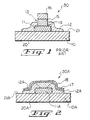
- Figure 1 is a side view shown in cross-section of a PRIOR ART semiconductor device over which our invention is an improvement.
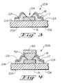
- Figure 2 is a side view in cross-section, similar to Figure 1, but showing our improved semiconductor device in an early stage of its manufacture.
- Figure 3 is a side view in cross-section, similar to Figure 2, showing our device in a later stage of its manufacture.
- Figure 4 is a side view in cross-section, similar to Figures 2 and 3, showing our finished device.
- the PRIOR ART IC device 30 in Figure 1 is composed of a silicon substrate 10 having a back non-circuit side 20 and a front side 21 on which ICs are formed. These active devices contain diodes and transistors which form an IC when interconnected by a patterned metallic layer (not shown). The metallic interconnections terminate at bond pads 11 located on the front circuit side 21 of device 30.
- the bond pads 11 are most commonly made of aluminum and provide the means of establishing electrical connection with the ICs. Techniques such as wire bonding, tape automated bonding (TAB), and flip chip bonding, provide the link between the bond pad(s) 11 and other individual devices which together form a complete electronic system.
- the surface of side 21 containing the ICs is coated with a primary passivation layer 12.
- the primary passivation layer 12 is an insulating layer over surface 21 to protect it from contaminants, moisture or particles.
- Devices usually employ a ceramic coating as layer 12 such as silicon oxides (SiO x ), silica (SiO 2 ), silicon carbide (SiC), silicon carbonitride (SiC x N y ), silicon oxycarbide (SiC x O y ), silicon oxycarbonitride (SiC x O y N z ), silicon nitride (Si x N y , i.e., Si 3 N 4 ), silicon oxynitride (Si 2 N 2 O), phosphosilicate glass (PSG), boron phosphorous silicate glass (BPSG), an organic film or a metal oxide from Group III of the periodic chart, such as gallium oxide (GaO x ).
- a ceramic coating such as silicon oxides
- these ceramic coatings are deposited by chemical vapor deposition (CVD), plasma enhanced chemical vapor deposition (PECVD), or physical vapor deposition (PVD) techniques.
- layer 12 is a PECVD film of silicon nitride or silicon oxynitride.
- layer 12 extends up and over the outer edges of the bond pad 11.
- a window 13 with an edge 14 is opened in layer 12 to expose the bond pad 11 metal.
- electrical connection is made by welding or soldering leads directly to the exposed area of aluminum bond pad 11, most typically, an intermediate metal layer 15 of copper, tin, lead, titanium or tungsten, is applied over the aluminum bond pad 11.
- Metal layer 15 provides chemical isolation for bond pad 11 and is used as a supporting surface for the gold or solder bumps 16 which function as a final electrical connection.
- the first step in providing this improved structure involves applying the flowable liquid resin composition as a coating to the surface of layer 12A, followed by heating the coating to a temperature sufficient to stabilize it, i.e., to convert the coating to a silica-containing ceramic layer 17.
- One type of flowable composition which can be used is a solution containing a hydridosiloxane resin which may contain units of the formula HSi(OH) x (OR) y O z/2 .
- R is independently an organic group or substituted organic group, which when bonded to silicon through the oxygen atom, forms a hydrolyzable substituent. Suitable R groups include alkyl groups such as methyl, ethyl, propyl, and butyl; aryl groups such as phenyl; and alkenyl groups such as allyl or vinyl.
- the value of x is 0-2; y is 0-2; z is 1-3; and the sum of x + y + z is 3.
- These resins may be fully condensed hydrogen silsesquioxane resins (HSiO 3/2 ) n , resins which are only partially hydrolyzed (i.e., containing some ⁇ SiOR), and/or resins which are partially condensed (i.e., containing some ⁇ SiOH).
- the resin may contain less than 10% of silicon atoms having either no hydrogen atoms, or two hydrogen atoms, which can occur during their formation or handling.
- Hydrogen silsesquioxane resins are ladder or cage polymers which are shown generally by the formula:
- n has a value of four or more.
- n has a bond arrangement for a silsesquioxane cubical octamer is shown below:
- n being ten or more
- double-stranded polysiloxanes of indefinitely higher molecular weight are formed, containing regular and repeated cross-ties in their extended structure.
- H-resins Hydrogen silsesquioxane resins
- US Patent 3,615,272 Hydrogen silsesquioxane resins
- ⁇ SiOH silanol
- US Patent 5,010,159 teaches another method of hydrolyzing hydridosilanes in an arylsulfonic acid hydrate hydrolysis medium to form the resin, which is then contacted with a neutralizing agent.
- silica precursor material which can be formed into the desired silica-containing ceramic layer 17
- another type of silica precursor material is a hydrolyzed or partially hydrolyzed compound of the formula R n Si(OR) 4-n in which R is the same as defined above and n is 0-3.
- R is the same as defined above and n is 0-3.
- Representative compounds are methyltriethoxysilane, phenyltriethoxysilane, diethyldiethoxysilane, methyltrimethoxysilane, dimethyldimethoxysilane, phenyltrimethoxysilane, vinyltrimethoxysilane, tetramethoxysilane, tetraethoxysilane, tetrapropoxysilane and tetrabutoxysilane.
- the silicon atoms therein are bonded to C, OH or OR groups, but a substantial portion of the material is believed to be condensed in the form of soluble Si-O-Si resins.
- n 2 or 3
- n 2 or 3
- other silanes in which n is zero or one to prepare useful preceramic materials.
- BCB benzocyclobutene
- the flowable composition is stabilized, i.e., formed into silica-containing ceramic layer 17, by any known technique.
- a solution of a solvent and the preceramic resin is applied to layer 12A and the solvent is evaporated.
- This solution is formed by simply dissolving or dispersing the preceramic resin in the solvent or in a mixture of solvents.
- suitable solvents are aromatic hydrocarbons such as benzene or toluene; alkanes such as n-heptane or dodecane; ketones; cyclic polydimethylsiloxanes such as octamethylcyclo-tetrasiloxane and decamethylcyclopentasiloxane; esters or ethers.
- enough solvent is used to form a 0.1-85 weight percent solids solution of the resin, preferably 5-30 weight percent.
- Additional materials may be added to the flowable composition such as other preceramic materials or preceramic polymer precursors; oxides such as aluminum, titanium, zirconium, tantalum, niobium, vanadium, boron, or phosphorous, at 0.1-50 weight percent; catalysts such as platinum, rhodium, or copper, at 5-500 parts per million based on the weight of the resin; or fillers.
- the preceramic resin solution is then coated on the surface of layer 12A by spin coating, dip coating, spray coating, or flow coating. This is followed by evaporation of the solvent to form preceramic layer 17. Although a solution approach is most desirable, melt coating can also be employed.
- the preceramic resin is then stabilized, i.e., converted into silica-containing ceramic layer 17, by heating it to a temperature sufficient for ceramification. Generally, this temperature is in the range of 50-800°C., preferably 50-600°C., more preferably 100-400°C.
- the time of heating is that sufficient to form a silica-containing ceramic layer 17, and is generally up to 6 hours, with a range of 5 minutes to 3 hours being most preferred.
- Heating may be conducted at any effective atmospheric pressure from vacuum to superatmospheric and under any effective oxidizing or non-oxidizing gaseous environment.
- gases include air, O 2 , inert gases such as N 2 , ammonia, amines, moisture, N 2 O and hydrogen.
- Any heating means is suitable such as a convection oven, rapid thermal processor, hot plate, radiant or microwave energy. The rate of heating is not critical but it is most practical to heat as rapidly as possible.
- Silica-containing ceramic layer 17 may contain amorphous silica (SiO 2 ) and amorphous silica-like materials that are not fully free of residual carbon, silanol ( ⁇ SiOH) and/or hydrogen.
- the resulting amorphous silicon oxide layer 17 can be porous or condensed, depending upon the temperature used for its ceramification.
- the stabilized layer 17 provides a more planar surface above the bond pad 11A than the sharp edge 14 of window 13 employed in the PRIOR ART integrated circuit device 30 shown in Figure 1.
- a silicon carbide ceramic layer 18 is shown applied to the surface of amorphous silicon oxide layer 17.
- the layer 18 is applied by CVD techniques such as thermal chemical vapor deposition (TCVD), photochemical vapor deposition (PCVD), plasma enhanced chemical vapor deposition (PECVD), electron cyclotron resonance (ECR) or jet vapor deposition. Additionally, it is also applied by physical vapor deposition (PVD) techniques such as sputtering or electron beam evaporation. These processes involve the addition of energy in the form of heat or plasma to a vaporized species to cause the desired reaction or the focusing of energy on a solid sample of the material to cause its deposition.
- CVD thermal chemical vapor deposition
- PCVD photochemical vapor deposition
- PECVD plasma enhanced chemical vapor deposition
- ECR electron cyclotron resonance
- PVD physical vapor deposition
- PECVD plasma-adioxide deposition
- a precursor gas is reacted by passing it through a plasma field. Reactive species form and are focused at the substrate where they readily adhere.
- the advantage of a PECVD process over a TCVD process is that in PECVD, lower substrate temperatures, i.e., 50-400°C., are employed.
- Plasma used in PECVD processes is energy derived from electric discharges, electromagnetic fields in the radiofrequency or microwave range, lasers or particle beams. Preferred, however, is the use of radio frequency (i.e., 10 kHz to 10 2 MHz), or microwave energy (i.e., 0.1-10 GHz), at moderate power densities (i.e., 0.1-5 watts/cm 2 ) . Frequency, power and pressure are normally tailored to a particular precursor gas and equipment being employed.
- Suitable precursor gases include (1) mixtures of silanes or halosilanes such as trichlorosilane (HSiCl 3 ), with an alkane having 1-6 carbon atoms such as methane, ethane or propane; (2) an alkylsilane such as methylsilane (CH 3 SiH 3 ), dimethylsilane (CH 3 ) 2 SiH 2 , trimethylsilane (CH 3 ) 3 SiH or hexamethyldisilane (CH 3 ) 3 Si-Si(CH 3 ) 3 ; or (3) silacyclobutanes or disilacyclobutanes as described in US Patent 5,011,706.
- silanes or halosilanes such as trichlorosilane (HSiCl 3 ), with an alkane having 1-6 carbon atoms such as methane, ethane or propane
- an alkylsilane such as methylsilane (CH 3 SiH 3 ), dimethylsilane (CH 3
- silacyclobutanes (1) and disilacyclobutanes (2) are shown below, wherein R1 is hydrogen atom, fluorine atom or a hydrocarbon radical having 1-4 carbon atoms; and R2 is hydrogen atom or a hydrocarbon radical having 1-4 carbon atoms.
- R1 is hydrogen atom, fluorine atom or a hydrocarbon radical having 1-4 carbon atoms
- R2 is hydrogen atom or a hydrocarbon radical having 1-4 carbon atoms.
- One suitable disilacyclobutane is 1,3-dimethyl-1,3-disilacyclobutane shown in formula (3).
- silicon carbide ceramic layer 18 is the PECVD of trimethylsilane.
- the resulting amorphous silicon carbide ceramic layer 18 is mechanically and chemically robust and it readily protects semiconductor die 30A during KGD testing and handling.
- layer 18 forms a hermetic and electrical barrier over the surface of amorphous silicon oxide layer 17 and over surface 12A of semiconductor chip 30A.
- portions of the layers covering bond pad 11A can be removed by etching or partial etching to allow for attachment of leads to the bond pad or for application of additional conductive metal layers to the top of the bond pad.
- Etching is accomplished by dry etching using plasma, combined with wet etching with hydrofluoric acid and/or laser ablation.
- ceramic layers 17 and 18 are applied in a manner so as not to coat bond pad 11A in its entirety, in which case etching or partial etching is not required.
- the resulting tapered opening 13A in Figure 3 allows for a more uniform deposition of the diffusion barrier metal layer 15A seen in Figure 4, increasing its stability and its ability to prevent interaction with the underlaying aluminum of bond pad 11A.
- bond pad 11A is sealed by covering it with a non-corroding conductive metal layer 16A, although in some cases, a corrodible material can be employed.
- Layer 16A is most preferably a gold or solder (95Pb-5Sn) bump, although it can be any metal which is stable in the environment, electrically conductive and useful for interconnecting circuits of semiconductor die 30A.
- Suitable materials include copper, silver, silver filled epoxy, silver-filled polyimide, silver-filled polysiloxanes, silver-filled silicone elastomers or silver-filled silicone resins.
- Methods for applying conductive metal layer 16A are sputtering and electron beam evaporation. It is also applied by merely dispensing the metallic material directly onto the top of metal layer 15A or directly onto the top of bond pad 11A where a metal layer 15A is not present.
- the part to be coated i.e., the semiconductor die 30A
- the part to be coated is placed in an evacuated chamber in close proximity to a flat plate of the coating material, i.e., the metal.
- the flat plate is the target and is bombarded by a beam of electrons.
- the electrons knock atoms off the target onto the surface of the part facing it. Only portions of the part directly exposed to the target are coated.
- the advantages of sputtering are that purity of a coating is controlled and parts are not required to be heated during the process. Techniques involving heat such as electron beam heating can also be employed.
- the aluminum metal of bond pad 11A is often incompatible with metallic material used to form conductive layer 16A.
- a nonconducting alloy forms (for example, gold and aluminum alloys form "purple plague"), which can also damage the circuit.
- diffusion barrier metal layer 15A is applied between bond pad 11A and layer 16A.
- Metals for forming layer 15A include nickel, copper, titanium, tungsten, vanadium, chromium, platinum and palladium; and metal alloys such as titanium-tungsten (TiW) or titanium nitride (TiN).
- Metal layer 15A is easily applied by sputtering the metal or metal alloy onto the exposed surface of bond pad 11A, or by dispensing metallic material directly onto the top of bond pad 11A.
- chips 30A are then interconnected with one another, or connected with a lead frame, circuit board or other external component. These interconnections are made using conventional leads, TAB or "flip chip” processing techniques. After interconnection, chip 30A is then packaged by embedding it within an organic encapsulant such as a polyimide; an epoxy; or a polyxylylene sold under the trademark PARYLENE® by Union Carbide Corporation, Danbury, Connecticut. Chip 30A can also be embedded within a silicone encapsulant, or included in a plastic package for additional protection, if desired.
- organic encapsulant such as a polyimide; an epoxy; or a polyxylylene sold under the trademark PARYLENE® by Union Carbide Corporation, Danbury, Connecticut.
- Chip 30A can also be embedded within a silicone encapsulant, or included in a plastic package for additional protection, if desired.
Landscapes
- Internal Circuitry In Semiconductor Integrated Circuit Devices (AREA)
- Testing Or Measuring Of Semiconductors Or The Like (AREA)
- Wire Bonding (AREA)
Applications Claiming Priority (2)
| Application Number | Priority Date | Filing Date | Title |
|---|---|---|---|
| US08/679,590 US5693565A (en) | 1996-07-15 | 1996-07-15 | Semiconductor chips suitable for known good die testing |
| US679590 | 1996-07-15 |
Publications (1)
| Publication Number | Publication Date |
|---|---|
| EP0820097A1 true EP0820097A1 (de) | 1998-01-21 |
Family
ID=24727516
Family Applications (1)
| Application Number | Title | Priority Date | Filing Date |
|---|---|---|---|
| EP97305252A Withdrawn EP0820097A1 (de) | 1996-07-15 | 1997-07-15 | Halbleiterchips mit Anschlussfläschen zur Verbesserung des Chip-Testens |
Country Status (5)
| Country | Link |
|---|---|
| US (1) | US5693565A (de) |
| EP (1) | EP0820097A1 (de) |
| JP (1) | JPH1098042A (de) |
| KR (1) | KR980012212A (de) |
| TW (1) | TW330321B (de) |
Cited By (2)
| Publication number | Priority date | Publication date | Assignee | Title |
|---|---|---|---|---|
| US7741560B2 (en) | 2005-07-22 | 2010-06-22 | Honda Motor Co., Ltd. | Chalcopyrite solar cell |
| US9835653B2 (en) | 2014-05-13 | 2017-12-05 | International Business Machines Corporation | Solder bump array probe tip structure for laser cleaning |
Families Citing this family (58)
| Publication number | Priority date | Publication date | Assignee | Title |
|---|---|---|---|---|
| JP3082688B2 (ja) * | 1996-11-05 | 2000-08-28 | ヤマハ株式会社 | 配線形成法 |
| US6030453A (en) * | 1997-03-04 | 2000-02-29 | Motorola, Inc. | III-V epitaxial wafer production |
| US5892270A (en) * | 1997-05-23 | 1999-04-06 | Samsung Electronics Co., Ltd. | Chip on board assembly without wire bonding |
| TW354417B (en) * | 1997-10-18 | 1999-03-11 | United Microelectronics Corp | A method for forming a planarized dielectric layer |
| US6875681B1 (en) * | 1997-12-31 | 2005-04-05 | Intel Corporation | Wafer passivation structure and method of fabrication |
| US6162652A (en) * | 1997-12-31 | 2000-12-19 | Intel Corporation | Process for sort testing C4 bumped wafers |
| US6018002A (en) * | 1998-02-06 | 2000-01-25 | Dow Corning Corporation | Photoluminescent material from hydrogen silsesquioxane resin |
| US6452271B2 (en) | 1998-07-31 | 2002-09-17 | Micron Technology, Inc. | Interconnect component for a semiconductor die including a ruthenium layer and a method for its fabrication |
| US6179659B1 (en) | 1998-08-11 | 2001-01-30 | Micron Technology, Inc. | Electrical contact device and associated method of manufacture |
| US6515355B1 (en) * | 1998-09-02 | 2003-02-04 | Micron Technology, Inc. | Passivation layer for packaged integrated circuits |
| US6621703B2 (en) * | 1998-10-07 | 2003-09-16 | Electro-Dyn Electronics Corporation | Automotive bridge rectifier assembly with thermal protection |
| US6297561B1 (en) * | 1999-05-26 | 2001-10-02 | United Microelectronics Corp. | Semiconductor chip |
| JP3387478B2 (ja) * | 1999-06-30 | 2003-03-17 | セイコーエプソン株式会社 | 半導体装置およびその製造方法 |
| US6403457B2 (en) * | 1999-08-25 | 2002-06-11 | Micron Technology, Inc. | Selectively coating bond pads |
| US6391163B1 (en) | 1999-09-27 | 2002-05-21 | Applied Materials, Inc. | Method of enhancing hardness of sputter deposited copper films |
| US6432819B1 (en) | 1999-09-27 | 2002-08-13 | Applied Materials, Inc. | Method and apparatus of forming a sputtered doped seed layer |
| US6593653B2 (en) * | 1999-09-30 | 2003-07-15 | Novellus Systems, Inc. | Low leakage current silicon carbonitride prepared using methane, ammonia and silane for copper diffusion barrier, etchstop and passivation applications |
| US6191023B1 (en) * | 1999-11-18 | 2001-02-20 | Taiwan Semiconductor Manufacturing Company | Method of improving copper pad adhesion |
| US6572974B1 (en) | 1999-12-06 | 2003-06-03 | The Regents Of The University Of Michigan | Modification of infrared reflectivity using silicon dioxide thin films derived from silsesquioxane resins |
| US6261939B1 (en) * | 1999-12-23 | 2001-07-17 | Philips Semiconductors, Inc. | Pad metallization over active circuitry |
| US6936900B1 (en) | 2000-05-04 | 2005-08-30 | Osemi, Inc. | Integrated transistor devices |
| US6451711B1 (en) * | 2000-05-04 | 2002-09-17 | Osemi, Incorporated | Epitaxial wafer apparatus |
| US6670651B1 (en) | 2000-05-04 | 2003-12-30 | Osemi, Inc. | Metal sulfide-oxide semiconductor transistor devices |
| US6445015B1 (en) | 2000-05-04 | 2002-09-03 | Osemi, Incorporated | Metal sulfide semiconductor transistor devices |
| FR2808920B1 (fr) * | 2000-05-10 | 2003-10-03 | Gemplus Card Int | Procede de protection de puces de circuit integre |
| US6358834B1 (en) * | 2000-10-16 | 2002-03-19 | Orient Semiconductor Electronics Limited | Method of forming bumps on wafers or substrates |
| US6537733B2 (en) * | 2001-02-23 | 2003-03-25 | Applied Materials, Inc. | Method of depositing low dielectric constant silicon carbide layers |
| US6515488B1 (en) * | 2001-05-07 | 2003-02-04 | Stmicroelectronics, Inc. | Fingerprint detector with scratch resistant surface and embedded ESD protection grid |
| US6563226B2 (en) | 2001-05-23 | 2003-05-13 | Motorola, Inc. | Bonding pad |
| US6737353B2 (en) * | 2001-06-19 | 2004-05-18 | Advanced Semiconductor Engineering, Inc. | Semiconductor device having bump electrodes |
| JP3761461B2 (ja) * | 2001-12-13 | 2006-03-29 | Necエレクトロニクス株式会社 | 半導体装置の製造方法 |
| US6914332B2 (en) * | 2002-01-25 | 2005-07-05 | Texas Instruments Incorporated | Flip-chip without bumps and polymer for board assembly |
| US6989556B2 (en) * | 2002-06-06 | 2006-01-24 | Osemi, Inc. | Metal oxide compound semiconductor integrated transistor devices with a gate insulator structure |
| US7187045B2 (en) * | 2002-07-16 | 2007-03-06 | Osemi, Inc. | Junction field effect metal oxide compound semiconductor integrated transistor devices |
| JP2004214594A (ja) * | 2002-11-15 | 2004-07-29 | Sharp Corp | 半導体装置およびその製造方法 |
| US20040102022A1 (en) * | 2002-11-22 | 2004-05-27 | Tongbi Jiang | Methods of fabricating integrated circuitry |
| DE10262143B4 (de) * | 2002-12-20 | 2011-01-20 | Ksg Leiterplatten Gmbh | Lichtemittierende Anordnung |
| US7453254B2 (en) * | 2003-07-25 | 2008-11-18 | Paragon Ag | Microstructured chemical sensor |
| WO2005048318A2 (en) * | 2003-11-17 | 2005-05-26 | Osemi, Inc. | Nitride metal oxide semiconductor integrated transistor devices |
| US20080282983A1 (en) * | 2003-12-09 | 2008-11-20 | Braddock Iv Walter David | High Temperature Vacuum Evaporation Apparatus |
| TWI245345B (en) * | 2005-02-17 | 2005-12-11 | Touch Micro System Tech | Method of forming a wear-resistant dielectric layer |
| US8361227B2 (en) * | 2006-09-26 | 2013-01-29 | Ii-Vi Incorporated | Silicon carbide single crystals with low boron content |
| US8858709B1 (en) | 2006-04-11 | 2014-10-14 | Ii-Vi Incorporated | Silicon carbide with low nitrogen content and method for preparation |
| JP2010510685A (ja) * | 2006-11-20 | 2010-04-02 | スリーエム イノベイティブ プロパティズ カンパニー | Led光源用の光学接着組成物 |
| US7682959B2 (en) * | 2007-03-21 | 2010-03-23 | Stats Chippac, Ltd. | Method of forming solder bump on high topography plated Cu |
| WO2008122292A1 (en) * | 2007-04-04 | 2008-10-16 | Ecole Polytechnique Federale De Lausanne (Epfl) | Diffusion-barrier coating for protection of moisture and oxygen sensitive devices |
| US8143729B2 (en) * | 2008-01-25 | 2012-03-27 | International Rectifier Corporation | Autoclave capable chip-scale package |
| JP4862017B2 (ja) * | 2008-07-10 | 2012-01-25 | ルネサスエレクトロニクス株式会社 | 中継基板、その製造方法、プローブカード |
| US20110012239A1 (en) * | 2009-07-17 | 2011-01-20 | Qualcomm Incorporated | Barrier Layer On Polymer Passivation For Integrated Circuit Packaging |
| NL2004142C2 (nl) | 2010-01-25 | 2011-07-26 | Mci Mirror Controls Int Nl Bv | Buitenspiegeleenheid, spiegeldrager, werkwijze voor montage van een buitenspiegeleenheid. |
| KR101678054B1 (ko) * | 2010-06-28 | 2016-11-22 | 삼성전자 주식회사 | 반도체 패키지 및 그 반도체 패키지 제조방법 |
| US8242613B2 (en) | 2010-09-01 | 2012-08-14 | Freescale Semiconductor, Inc. | Bond pad for semiconductor die |
| US8569167B2 (en) * | 2011-03-29 | 2013-10-29 | Micron Technology, Inc. | Methods for forming a semiconductor structure |
| US8501613B2 (en) * | 2011-07-07 | 2013-08-06 | Taiwan Semiconductor Manufacturing Company, Ltd. | UBM etching methods for eliminating undercut |
| US9287165B2 (en) * | 2013-06-26 | 2016-03-15 | Infineon Technologies Ag | Semiconductor device and method for producing the same |
| US9837278B2 (en) * | 2014-02-27 | 2017-12-05 | Taiwan Semiconductor Manufacturing Company Ltd. | Wafer level chip scale package and method of manufacturing the same |
| KR102594921B1 (ko) * | 2016-10-31 | 2023-10-26 | 엘지디스플레이 주식회사 | 유기 발광 표시 장치 |
| US20230361063A1 (en) * | 2020-09-23 | 2023-11-09 | Nippon Telegraph And Telephone Corporation | Semiconductor Integrated Circuit |
Citations (8)
| Publication number | Priority date | Publication date | Assignee | Title |
|---|---|---|---|---|
| JPS61134050A (ja) * | 1984-12-04 | 1986-06-21 | Nippon Denso Co Ltd | 集積回路素子 |
| JPH03185731A (ja) * | 1989-12-14 | 1991-08-13 | Nec Corp | 半導体装置 |
| JPH04152634A (ja) * | 1990-10-17 | 1992-05-26 | Hitachi Ltd | 半導体集積回路装置 |
| US5136364A (en) * | 1991-06-12 | 1992-08-04 | National Semiconductor Corporation | Semiconductor die sealing |
| EP0589678A2 (de) * | 1992-09-23 | 1994-03-30 | Dow Corning Corporation | Hermetischer Schutz für integrierte Schaltungen |
| EP0637070A1 (de) * | 1993-07-28 | 1995-02-01 | The Whitaker Corporation | Von der Peripherie-unabhängiges präzises Positionsglied für einen Halbleiterchip und Herstellungsverfahren dafür |
| EP0661742A1 (de) * | 1993-12-29 | 1995-07-05 | Dow Corning Corporation | Integrierte Schaltungen mit Passivierung und Metallisierung für hermetischen Schutz |
| US5483741A (en) * | 1993-09-03 | 1996-01-16 | Micron Technology, Inc. | Method for fabricating a self limiting silicon based interconnect for testing bare semiconductor dice |
Family Cites Families (14)
| Publication number | Priority date | Publication date | Assignee | Title |
|---|---|---|---|---|
| US3615272A (en) * | 1968-11-04 | 1971-10-26 | Dow Corning | Condensed soluble hydrogensilsesquioxane resin |
| JPS59178749A (ja) * | 1983-03-30 | 1984-10-11 | Fujitsu Ltd | 配線構造体 |
| JPS6086017A (ja) * | 1983-10-17 | 1985-05-15 | Fujitsu Ltd | ポリハイドロジエンシルセスキオキサンの製法 |
| JPS63107122A (ja) * | 1986-10-24 | 1988-05-12 | Fujitsu Ltd | 凹凸基板の平坦化方法 |
| JP2633586B2 (ja) * | 1987-10-21 | 1997-07-23 | 株式会社東芝 | バンプ構造を有する半導体装置 |
| US5011706A (en) * | 1989-04-12 | 1991-04-30 | Dow Corning Corporation | Method of forming coatings containing amorphous silicon carbide |
| US4999397A (en) * | 1989-07-28 | 1991-03-12 | Dow Corning Corporation | Metastable silane hydrolyzates and process for their preparation |
| US5010159A (en) * | 1989-09-01 | 1991-04-23 | Dow Corning Corporation | Process for the synthesis of soluble, condensed hydridosilicon resins containing low levels of silanol |
| US5130275A (en) * | 1990-07-02 | 1992-07-14 | Digital Equipment Corp. | Post fabrication processing of semiconductor chips |
| JP2533414B2 (ja) * | 1991-04-09 | 1996-09-11 | 三菱電機株式会社 | 半導体集積回路装置の配線接続構造およびその製造方法 |
| US5424652A (en) * | 1992-06-10 | 1995-06-13 | Micron Technology, Inc. | Method and apparatus for testing an unpackaged semiconductor die |
| US5376584A (en) * | 1992-12-31 | 1994-12-27 | International Business Machines Corporation | Process of making pad structure for solder ball limiting metallurgy having reduced edge stress |
| US5495667A (en) * | 1994-11-07 | 1996-03-05 | Micron Technology, Inc. | Method for forming contact pins for semiconductor dice and interconnects |
| US5597737A (en) * | 1995-11-03 | 1997-01-28 | Motorola Inc. | Method for testing and burning-in a semiconductor wafer |
-
1996
- 1996-07-15 US US08/679,590 patent/US5693565A/en not_active Expired - Fee Related
-
1997
- 1997-07-01 TW TW086109295A patent/TW330321B/zh active
- 1997-07-11 JP JP9185617A patent/JPH1098042A/ja not_active Withdrawn
- 1997-07-15 EP EP97305252A patent/EP0820097A1/de not_active Withdrawn
- 1997-07-15 KR KR1019970032837A patent/KR980012212A/ko not_active Withdrawn
Patent Citations (8)
| Publication number | Priority date | Publication date | Assignee | Title |
|---|---|---|---|---|
| JPS61134050A (ja) * | 1984-12-04 | 1986-06-21 | Nippon Denso Co Ltd | 集積回路素子 |
| JPH03185731A (ja) * | 1989-12-14 | 1991-08-13 | Nec Corp | 半導体装置 |
| JPH04152634A (ja) * | 1990-10-17 | 1992-05-26 | Hitachi Ltd | 半導体集積回路装置 |
| US5136364A (en) * | 1991-06-12 | 1992-08-04 | National Semiconductor Corporation | Semiconductor die sealing |
| EP0589678A2 (de) * | 1992-09-23 | 1994-03-30 | Dow Corning Corporation | Hermetischer Schutz für integrierte Schaltungen |
| EP0637070A1 (de) * | 1993-07-28 | 1995-02-01 | The Whitaker Corporation | Von der Peripherie-unabhängiges präzises Positionsglied für einen Halbleiterchip und Herstellungsverfahren dafür |
| US5483741A (en) * | 1993-09-03 | 1996-01-16 | Micron Technology, Inc. | Method for fabricating a self limiting silicon based interconnect for testing bare semiconductor dice |
| EP0661742A1 (de) * | 1993-12-29 | 1995-07-05 | Dow Corning Corporation | Integrierte Schaltungen mit Passivierung und Metallisierung für hermetischen Schutz |
Non-Patent Citations (4)
| Title |
|---|
| GRISH CHANDRA: "Low temperature ceramic coatings for environmental protection of integrated circuits", ELECTRONIC PACKAGING MATERIAL SCIENCE SYMPOSIUM, 26 November 1990 (1990-11-26) - 29 November 1990 (1990-11-29), BOSTON, US, pages 97 - 108, XP002044990 * |
| PATENT ABSTRACTS OF JAPAN vol. 010, no. 329 (E - 452) 8 November 1986 (1986-11-08) * |
| PATENT ABSTRACTS OF JAPAN vol. 015, no. 442 (E - 1131) 11 November 1991 (1991-11-11) * |
| PATENT ABSTRACTS OF JAPAN vol. 016, no. 435 (E - 1263) 10 September 1992 (1992-09-10) * |
Cited By (3)
| Publication number | Priority date | Publication date | Assignee | Title |
|---|---|---|---|---|
| US7741560B2 (en) | 2005-07-22 | 2010-06-22 | Honda Motor Co., Ltd. | Chalcopyrite solar cell |
| US9835653B2 (en) | 2014-05-13 | 2017-12-05 | International Business Machines Corporation | Solder bump array probe tip structure for laser cleaning |
| US10571490B2 (en) | 2014-05-13 | 2020-02-25 | International Business Machines Corporation | Solder bump array probe tip structure for laser cleaning |
Also Published As
| Publication number | Publication date |
|---|---|
| US5693565A (en) | 1997-12-02 |
| TW330321B (en) | 1998-04-21 |
| KR980012212A (ko) | 1998-04-30 |
| JPH1098042A (ja) | 1998-04-14 |
Similar Documents
| Publication | Publication Date | Title |
|---|---|---|
| US5693565A (en) | Semiconductor chips suitable for known good die testing | |
| US5563102A (en) | Method of sealing integrated circuits | |
| US5825078A (en) | Hermetic protection for integrated circuits | |
| EP0590781B1 (de) | Verfahren zur Herstellung einer integrierten Schaltung mit einem auf einer Keramikschicht basierenden Schutz | |
| US6368899B1 (en) | Electronic device packaging | |
| US5780163A (en) | Multilayer coating for microelectronic devices | |
| EP0834489A1 (de) | Dicke opake keramische Beschichtungen | |
| KR20020002446A (ko) | 중합체 재료에 대한 점착성이 강화된 반도체 장치의보호용 오버코트 및 그 제조 방법 | |
| US20080079176A1 (en) | Method and structure to enhance temperature/humidity/bias performance of semiconductor devices by surface modification | |
| CN100342512C (zh) | 利用经反应的硼硅酸盐混合物的连结结构 | |
| US20030153196A1 (en) | Method for reducing fluorine induced defects on a bonding pad surface | |
| EP0661742B1 (de) | Verfahren zur Passivierung einer integrierten Schaltung | |
| Kubacki | Low temperature plasma deposition of silicon nitride to produce ultra-reliable, high performance, low cost sealed chip-on-board (SCOB) assemblies | |
| EP0590780B1 (de) | Verfahren zur Herstellung einer integrierten Schaltung mit einem auf einer Keramikschicht basierenden hermetischen Schutz | |
| EP0588577A2 (de) | Hermetisch abgedichtete integrierte Schaltungen | |
| JPH0925179A (ja) | シリカと金の付着方法 | |
| JP2674670B2 (ja) | 半導体装置の製造方法 | |
| CN100390970C (zh) | 提高半导体器件的温度/湿度/偏压性能的方法和结构 | |
| JPH01307227A (ja) | 微細加工方法 |
Legal Events
| Date | Code | Title | Description |
|---|---|---|---|
| PUAI | Public reference made under article 153(3) epc to a published international application that has entered the european phase |
Free format text: ORIGINAL CODE: 0009012 |
|
| AK | Designated contracting states |
Kind code of ref document: A1 Designated state(s): DE FR GB IT NL |
|
| AX | Request for extension of the european patent |
Free format text: AL;LT;LV;RO;SI |
|
| 17P | Request for examination filed |
Effective date: 19980211 |
|
| AKX | Designation fees paid |
Free format text: DE FR GB IT NL |
|
| RBV | Designated contracting states (corrected) |
Designated state(s): DE FR GB IT NL |
|
| 17Q | First examination report despatched |
Effective date: 19990531 |
|
| STAA | Information on the status of an ep patent application or granted ep patent |
Free format text: STATUS: THE APPLICATION HAS BEEN WITHDRAWN |
|
| 18W | Application withdrawn |
Withdrawal date: 20010712 |