EP0820099A2 - Dispositif semi-conducteur empaqueté et méthode de fabrication associée - Google Patents
Dispositif semi-conducteur empaqueté et méthode de fabrication associée Download PDFInfo
- Publication number
- EP0820099A2 EP0820099A2 EP97111954A EP97111954A EP0820099A2 EP 0820099 A2 EP0820099 A2 EP 0820099A2 EP 97111954 A EP97111954 A EP 97111954A EP 97111954 A EP97111954 A EP 97111954A EP 0820099 A2 EP0820099 A2 EP 0820099A2
- Authority
- EP
- European Patent Office
- Prior art keywords
- package
- electrode
- lsi chip
- chip
- wafer
- Prior art date
- Legal status (The legal status is an assumption and is not a legal conclusion. Google has not performed a legal analysis and makes no representation as to the accuracy of the status listed.)
- Withdrawn
Links
Images

Classifications
-
- H—ELECTRICITY
- H10—SEMICONDUCTOR DEVICES; ELECTRIC SOLID-STATE DEVICES NOT OTHERWISE PROVIDED FOR
- H10W—GENERIC PACKAGES, INTERCONNECTIONS, CONNECTORS OR OTHER CONSTRUCTIONAL DETAILS OF DEVICES COVERED BY CLASS H10
- H10W76/00—Containers; Fillings or auxiliary members therefor; Seals
- H10W76/10—Containers or parts thereof
-
- H—ELECTRICITY
- H10—SEMICONDUCTOR DEVICES; ELECTRIC SOLID-STATE DEVICES NOT OTHERWISE PROVIDED FOR
- H10W—GENERIC PACKAGES, INTERCONNECTIONS, CONNECTORS OR OTHER CONSTRUCTIONAL DETAILS OF DEVICES COVERED BY CLASS H10
- H10W99/00—Subject matter not provided for in other groups of this subclass
-
- H—ELECTRICITY
- H10—SEMICONDUCTOR DEVICES; ELECTRIC SOLID-STATE DEVICES NOT OTHERWISE PROVIDED FOR
- H10W—GENERIC PACKAGES, INTERCONNECTIONS, CONNECTORS OR OTHER CONSTRUCTIONAL DETAILS OF DEVICES COVERED BY CLASS H10
- H10W20/00—Interconnections in chips, wafers or substrates
- H10W20/01—Manufacture or treatment
- H10W20/021—Manufacture or treatment of interconnections within wafers or substrates
- H10W20/023—Manufacture or treatment of interconnections within wafers or substrates the interconnections being through-semiconductor vias
-
- H—ELECTRICITY
- H10—SEMICONDUCTOR DEVICES; ELECTRIC SOLID-STATE DEVICES NOT OTHERWISE PROVIDED FOR
- H10W—GENERIC PACKAGES, INTERCONNECTIONS, CONNECTORS OR OTHER CONSTRUCTIONAL DETAILS OF DEVICES COVERED BY CLASS H10
- H10W20/00—Interconnections in chips, wafers or substrates
- H10W20/20—Interconnections within wafers or substrates, e.g. through-silicon vias [TSV]
-
- H—ELECTRICITY
- H10—SEMICONDUCTOR DEVICES; ELECTRIC SOLID-STATE DEVICES NOT OTHERWISE PROVIDED FOR
- H10W—GENERIC PACKAGES, INTERCONNECTIONS, CONNECTORS OR OTHER CONSTRUCTIONAL DETAILS OF DEVICES COVERED BY CLASS H10
- H10W70/00—Package substrates; Interposers; Redistribution layers [RDL]
- H10W70/60—Insulating or insulated package substrates; Interposers; Redistribution layers
- H10W70/67—Insulating or insulated package substrates; Interposers; Redistribution layers characterised by their insulating layers or insulating parts
- H10W70/68—Shapes or dispositions thereof
Definitions
- the present invention relates to a packaged semiconductor device in which a package for mounting high-speed LSI elements at a high density is made of glass or a ceramic, and a method of manufacturing the same.
- the bare-chip mounting method called LLC connection or FC connection has been developed, as described above.
- FC connection In order to decrease the cost, the bare-chip mounting method called LLC connection or FC connection has been developed, as described above.
- this method how to inspect a bare chip poses a problem. Since an inspection process in the bare-chip level has not been established yet, sometimes the semiconductor manufacturer cannot guarantee the defectiveness/non-defectiveness of the chip to the system manufacturer. If a plurality of defective chips are mixedly mounted on the board, the board yield is degraded immediately. A chip not protected by the package cannot be handled well by the system manufacturer. Furthermore, a major problem exists as to how to manufacture a substrate having electrodes with the same precision as that of the small-pitch electrodes of the chips at a low cost.
- chip size package or chip scale package
- a package close to the chip size is fabricated.
- An Si chip is connected to this package without using leads, and the Si chip together with the package is further connected to a board.
- the problem of chip protection and inspection is solved, since the board is merely replaced with the chip size package, the problem of whether a package that can realize leadless connection at a low cost still remains unsolved.
- the present invention has been made in view of the above situation of the conventional technique, and has as its object to provide a packaged semiconductor device that serves as a wafer reinforcing member along with an increase in diameter of Si wafers, and enables leadless connection for an LSI chip and a board with a low-cost means while keeping completely the same size as that of the LSI chip which is to be mounted and held, and a method of manufacturing the same.
- a packaged semiconductor device comprising an LSI chip, a chip size package integrally bonded to the LSI chip to mount and hold the LSI chip thereon in order to connect an electrode of a board on which the LSI chip is to be mounted and an electrode of the LSI chip to each other, an electrode formed on a surface of the package opposite to a surface thereof which is bonded to the LSI chip, so as to be connected to the electrode of the board, at least one through hole formed to extend through the LSI chip and the package, and a connecting conductor formed to extend through the through hole in order to connect the electrode of the package and the electrode of the LSI package to each other.
- the package is made of glass or a ceramic having a thermal expansion coefficient close to that of an Si wafer constituting the LSI chip.
- this material is preferably SiO 2 -based glass, glass ceramic, alumina, mullite, cordierite, aluminum nitride, or the like.
- glass As an adhesive for bonding the LSI chip and the package to each other, glass is used.
- glass having a low softening temperature and capable of maintaining a viscosity at about 1,000°C is preferable.
- the package is preferably formed of a multilayer substrate.
- a method of manufacturing a packaged semiconductor device having a chip size package integrally formed with an LSI chip on which an integrated circuit is formed comprising the steps of forming, on a substrate that forms the package, an electrode to be connected to an electrode of a board on which the packaged semiconductor device is to be mounted, bonding an Si wafer to a surface of the substrate opposite to a surface where the electrode is formed, forming a predetermined integrated circuit on a surface of the bonded Si wafer opposite to a bonded surface, measuring a positional relationship between a position of an electrode of the formed integrated circuit and a position of the electrode formed on the package by using a transmission electromagnetic wave, forming at least one through hole at a position set based on the measured positional relationship so as to extend through the LSI chip and the package, forming a conductor that connects the electrode of the integrated circuit and the electrode of the package through the formed through hole, and cutting the package and the Si wafer that are bonded to each other into a pre
- an ultraviolet beam is used as the transmission electromagnetic wave.
- the glass or ceramic multilayer substrate is adhered to the Si wafer in its manufacturing process, its mechanical strength is reinforced.
- the through hole is formed through alignment using the transmission electromagnetic wave, e.g., an ultraviolet beam, even if the positional precision of the electrode of the substrate is degraded to be slightly different from that of the electrode of the LSI, an open defect does not occur due to conductor connection through the through hole.
- the transmission electromagnetic wave e.g., an ultraviolet beam
- the glass or ceramic package substrate to be bonded serves as the reinforcing member of the Si wafer, a large-diameter wafer can be used without increasing the thickness. This realizes a low-cost process for a large-diameter wafer.
- a plurality of silicon wafers can be adhered on a large-size multilayer substrate and the resultant structure can be processed with the process for a large-diameter wafer.
- the electrode of the Si wafer and the electrode of the package substrate to be connected to the board can be connected to each other with the connecting conductor through the through hole, high positional precision is not required for the electrode unlike in leadless chip connection. Since the minimum distance between the electrodes to be connected to the board can be set larger than that of the LSI chip, the mounting cost can be decreased even though the chip size package is employed. Also, inspection of a chip before mounting is possible. A high-reliability, low-cost chip size packaged semiconductor device can therefore be provided.
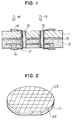
- Fig. 1 is a schematic sectional view of a packaged semiconductor device according to an embodiment of the present invention.
- reference numeral 11 denotes an LSI chip formed on an Si wafer and divided; 12, a chip size package formed by dividing a multilayer substrate; 13, a glass adhesion layer; 14, an electrode on the LSI chip; 15, through holes; 16, an electrode on the chip size packaged semiconductor; 17, a connecting conductor; 18, an ultraviolet beam; and 19, a laser beam.
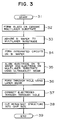
- Fig. 2 is a schematic perspective view of a glass or ceramic multilayer substrate to which the Si wafer of the present invention is bonded. Referring to Fig.
- FIG. 2 is a flow chart of a method of manufacturing a packaged semiconductor device according to the present invention. Referring to Fig. 3, reference numerals S31 to S39 denote the respective steps.
- Fig. 4 is a schematic perspective view showing a state wherein packages 42 of the present invention respectively bonded with the LSI chips 41 are mounted on a board 43.
- the glass or ceramic chip size package 12 as a multilayer substrate is integrated to the LSI chip 11 as it is completely bonded to the LSI chip 11 through the glass adhesion layer 13.
- the glass or ceramic multilayer substrate 22 shown in Fig. 2, which is bonded with the Si wafer 21 is divided at the cutting lines 23, thereby fabricating packaged semiconductors of the present invention.
- the electrode 14 formed on the integrated circuit of the LSI chip 11 is connected to the electrode 16, formed on the package 12 to be connected to the board, with the connecting conductor 17 through the through hole 15.
- a method of manufacturing a packaged semiconductor device according to the present invention will be described with reference to the manufacturing process flow chart shown in Fig. 3, and Figs. 1 and 2.
- the employed glass ceramic material is a composite of alumina and borosilicate glass having a thermal expansion coefficient of 5.0 ppm.
- AgPd having a weight ratio of 90/10 is used.
- a multilayer substrate was fabricated by using this glass ceramic material at the 12-inch wafer level, and an Si wafer was adhered to this substrate with SiO 2 -ZnO-type glass by heating the structure at a temperature of 1,100°C.
- the SiO 2 -ZnO-type glass has a softening temperature of 300°C and a thermal expansion coefficient of 4.0 ppm.
- Fig. 4 shows a state wherein the electrodes of the packages are connected to the mother board of a printed board through internal wiring of the packages. Even when this structure was subjected to a heat cycle of -45°C to 125°C for 500 times, an open short-circuiting defect did not occur.
Landscapes
- Wire Bonding (AREA)
Applications Claiming Priority (2)
| Application Number | Priority Date | Filing Date | Title |
|---|---|---|---|
| JP8189240A JP2783259B2 (ja) | 1996-07-18 | 1996-07-18 | 半導体パッケージとその製造方法 |
| JP189240/96 | 1996-07-18 |
Publications (2)
| Publication Number | Publication Date |
|---|---|
| EP0820099A2 true EP0820099A2 (fr) | 1998-01-21 |
| EP0820099A3 EP0820099A3 (fr) | 1999-03-10 |
Family
ID=16237967
Family Applications (1)
| Application Number | Title | Priority Date | Filing Date |
|---|---|---|---|
| EP97111954A Withdrawn EP0820099A3 (fr) | 1996-07-18 | 1997-07-14 | Dispositif semi-conducteur empaqueté et méthode de fabrication associée |
Country Status (4)
| Country | Link |
|---|---|
| US (2) | US5952712A (fr) |
| EP (1) | EP0820099A3 (fr) |
| JP (1) | JP2783259B2 (fr) |
| KR (1) | KR100269551B1 (fr) |
Cited By (2)
| Publication number | Priority date | Publication date | Assignee | Title |
|---|---|---|---|---|
| US6771786B1 (en) | 1999-07-28 | 2004-08-03 | Oticon A/S | Hearing aid including an integrated circuit |
| CN103094219A (zh) * | 2012-11-28 | 2013-05-08 | 贵州振华风光半导体有限公司 | 三维集成高密度厚膜多芯片组件的集成方法 |
Families Citing this family (39)
| Publication number | Priority date | Publication date | Assignee | Title |
|---|---|---|---|---|
| US6624505B2 (en) * | 1998-02-06 | 2003-09-23 | Shellcase, Ltd. | Packaged integrated circuits and methods of producing thereof |
| IL123207A0 (en) * | 1998-02-06 | 1998-09-24 | Shellcase Ltd | Integrated circuit device |
| US6090636A (en) * | 1998-02-26 | 2000-07-18 | Micron Technology, Inc. | Integrated circuits using optical waveguide interconnects formed through a semiconductor wafer and methods for forming same |
| US7179740B1 (en) * | 1999-05-03 | 2007-02-20 | United Microelectronics Corporation | Integrated circuit with improved interconnect structure and process for making same |
| US7030466B1 (en) | 1999-05-03 | 2006-04-18 | United Microelectronics Corporation | Intermediate structure for making integrated circuit device and wafer |
| US6429509B1 (en) * | 1999-05-03 | 2002-08-06 | United Microelectronics Corporation | Integrated circuit with improved interconnect structure and process for making same |
| US6338980B1 (en) * | 1999-08-13 | 2002-01-15 | Citizen Watch Co., Ltd. | Method for manufacturing chip-scale package and manufacturing IC chip |
| JP3494100B2 (ja) * | 2000-01-11 | 2004-02-03 | 富士通株式会社 | 半導体装置及びその実装方法 |
| US6801438B1 (en) | 2000-10-24 | 2004-10-05 | Touch Future Technolocy Ltd. | Electrical circuit and method of formation |
| TW523920B (en) * | 2000-11-18 | 2003-03-11 | Lenghways Technology Co Ltd | Integrated multi-channel communication passive device manufactured by using micro-electromechanical technique |
| AU2002216352A1 (en) * | 2000-12-21 | 2002-07-01 | Shellcase Ltd. | Packaged integrated circuits and methods of producing thereof |
| KR100370116B1 (ko) * | 2001-01-15 | 2003-01-30 | 앰코 테크놀로지 코리아 주식회사 | 반도체 패키지 및 그 제조방법 |
| US20020180029A1 (en) * | 2001-04-25 | 2002-12-05 | Hideki Higashitani | Semiconductor device with intermediate connector |
| US6809848B2 (en) * | 2001-06-01 | 2004-10-26 | Agere Systems Inc. | MEMS device |
| KR100385673B1 (ko) * | 2001-08-17 | 2003-06-02 | 신의승 | 회전추를 이용한 휴대가 간편한 원판 운동기구 |
| US6856007B2 (en) | 2001-08-28 | 2005-02-15 | Tessera, Inc. | High-frequency chip packages |
| US7038142B2 (en) * | 2002-01-24 | 2006-05-02 | Fujitsu Limited | Circuit board and method for fabricating the same, and electronic device |
| US6908784B1 (en) * | 2002-03-06 | 2005-06-21 | Micron Technology, Inc. | Method for fabricating encapsulated semiconductor components |
| JP4443865B2 (ja) * | 2002-06-24 | 2010-03-31 | 富士フイルム株式会社 | 固体撮像装置およびその製造方法 |
| US6599768B1 (en) * | 2002-08-20 | 2003-07-29 | United Epitaxy Co., Ltd. | Surface mounting method for high power light emitting diode |
| US6903442B2 (en) * | 2002-08-29 | 2005-06-07 | Micron Technology, Inc. | Semiconductor component having backside pin contacts |
| TWI227050B (en) * | 2002-10-11 | 2005-01-21 | Sanyo Electric Co | Semiconductor device and method for manufacturing the same |
| US7033664B2 (en) | 2002-10-22 | 2006-04-25 | Tessera Technologies Hungary Kft | Methods for producing packaged integrated circuit devices and packaged integrated circuit devices produced thereby |
| US7388294B2 (en) * | 2003-01-27 | 2008-06-17 | Micron Technology, Inc. | Semiconductor components having stacked dice |
| US6841883B1 (en) * | 2003-03-31 | 2005-01-11 | Micron Technology, Inc. | Multi-dice chip scale semiconductor components and wafer level methods of fabrication |
| US6972480B2 (en) * | 2003-06-16 | 2005-12-06 | Shellcase Ltd. | Methods and apparatus for packaging integrated circuit devices |
| WO2005004195A2 (fr) | 2003-07-03 | 2005-01-13 | Shellcase Ltd. | Procede et appareil d'encapsulation de circuits integres |
| US7224056B2 (en) * | 2003-09-26 | 2007-05-29 | Tessera, Inc. | Back-face and edge interconnects for lidded package |
| US20050116344A1 (en) * | 2003-10-29 | 2005-06-02 | Tessera, Inc. | Microelectronic element having trace formed after bond layer |
| DE102005006280B4 (de) * | 2005-02-10 | 2006-11-16 | Infineon Technologies Ag | Halbleiterbauteil mit einem Durchkontakt durch eine Gehäusemasse und Verfahren zur Herstellung desselben |
| US20060183270A1 (en) * | 2005-02-14 | 2006-08-17 | Tessera, Inc. | Tools and methods for forming conductive bumps on microelectronic elements |
| US8143095B2 (en) | 2005-03-22 | 2012-03-27 | Tessera, Inc. | Sequential fabrication of vertical conductive interconnects in capped chips |
| US7566853B2 (en) * | 2005-08-12 | 2009-07-28 | Tessera, Inc. | Image sensor employing a plurality of photodetector arrays and/or rear-illuminated architecture |
| US20070138644A1 (en) * | 2005-12-15 | 2007-06-21 | Tessera, Inc. | Structure and method of making capped chip having discrete article assembled into vertical interconnect |
| US7936062B2 (en) | 2006-01-23 | 2011-05-03 | Tessera Technologies Ireland Limited | Wafer level chip packaging |
| US8604605B2 (en) | 2007-01-05 | 2013-12-10 | Invensas Corp. | Microelectronic assembly with multi-layer support structure |
| JP4952372B2 (ja) * | 2007-05-23 | 2012-06-13 | 株式会社デンソー | 複合icパッケージ及びその製造方法 |
| KR100881199B1 (ko) | 2007-07-02 | 2009-02-05 | 삼성전자주식회사 | 관통전극을 구비하는 반도체 장치 및 이를 제조하는 방법 |
| KR100881400B1 (ko) | 2007-09-10 | 2009-02-02 | 주식회사 하이닉스반도체 | 반도체 패키지 및 이의 제조 방법 |
Family Cites Families (20)
| Publication number | Priority date | Publication date | Assignee | Title |
|---|---|---|---|---|
| US3560257A (en) * | 1967-01-03 | 1971-02-02 | Kollmorgen Photocircuits | Metallization of insulating substrates |
| US4499655A (en) * | 1981-03-18 | 1985-02-19 | General Electric Company | Method for making alignment-enhancing feed-through conductors for stackable silicon-on-sapphire |
| JPS6068687A (ja) * | 1983-09-26 | 1985-04-19 | Toshiba Corp | 半導体レ−ザ用パツケ−ジの製造方法 |
| US4733291A (en) * | 1985-11-15 | 1988-03-22 | American Telephone And Telegraph Company, At&T Bell Laboratories | Contact vias in semiconductor devices |
| JPS63107154A (ja) * | 1986-10-24 | 1988-05-12 | Hitachi Ltd | 樹脂封止型半導体装置 |
| US4991090A (en) * | 1987-05-18 | 1991-02-05 | International Business Machines Corporation | Posting out-of-sequence fetches |
| CA2002213C (fr) * | 1988-11-10 | 1999-03-30 | Iwona Turlik | Boitier de puce de circuits integres a haute performance et sa methode de fabrication |
| US5065228A (en) * | 1989-04-04 | 1991-11-12 | Olin Corporation | G-TAB having particular through hole |
| US5399898A (en) * | 1992-07-17 | 1995-03-21 | Lsi Logic Corporation | Multi-chip semiconductor arrangements using flip chip dies |
| US5198695A (en) * | 1990-12-10 | 1993-03-30 | Westinghouse Electric Corp. | Semiconductor wafer with circuits bonded to a substrate |
| US5229647A (en) * | 1991-03-27 | 1993-07-20 | Micron Technology, Inc. | High density data storage using stacked wafers |
| EP0575813B1 (fr) * | 1992-06-08 | 1996-12-27 | NEC Corporation | Substrat vitrocéramique à multi-couche et procédé pour sa fabrication |
| US5404044A (en) * | 1992-09-29 | 1995-04-04 | International Business Machines Corporation | Parallel process interposer (PPI) |
| US5406125A (en) * | 1993-04-15 | 1995-04-11 | Martin Marietta Corp. | Semiconductor device having a metalized via hole |
| US5386142A (en) * | 1993-05-07 | 1995-01-31 | Kulite Semiconductor Products, Inc. | Semiconductor structures having environmentally isolated elements and method for making the same |
| JPH07122589A (ja) * | 1993-10-22 | 1995-05-12 | Sharp Corp | 半導体装置及びその製造方法 |
| US5530288A (en) * | 1994-10-12 | 1996-06-25 | International Business Machines Corporation | Passive interposer including at least one passive electronic component |
| US5552633A (en) * | 1995-06-06 | 1996-09-03 | Martin Marietta Corporation | Three-dimensional multimodule HDI arrays with heat spreading |
| JP2905736B2 (ja) * | 1995-12-18 | 1999-06-14 | 株式会社エイ・ティ・アール光電波通信研究所 | 半導体装置 |
| US6063646A (en) * | 1998-10-06 | 2000-05-16 | Japan Rec Co., Ltd. | Method for production of semiconductor package |
-
1996
- 1996-07-18 JP JP8189240A patent/JP2783259B2/ja not_active Expired - Fee Related
-
1997
- 1997-07-14 EP EP97111954A patent/EP0820099A3/fr not_active Withdrawn
- 1997-07-16 KR KR1019970034044A patent/KR100269551B1/ko not_active Expired - Fee Related
- 1997-07-16 US US08/893,988 patent/US5952712A/en not_active Expired - Lifetime
-
1999
- 1999-06-15 US US09/333,578 patent/US6130111A/en not_active Expired - Lifetime
Cited By (2)
| Publication number | Priority date | Publication date | Assignee | Title |
|---|---|---|---|---|
| US6771786B1 (en) | 1999-07-28 | 2004-08-03 | Oticon A/S | Hearing aid including an integrated circuit |
| CN103094219A (zh) * | 2012-11-28 | 2013-05-08 | 贵州振华风光半导体有限公司 | 三维集成高密度厚膜多芯片组件的集成方法 |
Also Published As
| Publication number | Publication date |
|---|---|
| JPH1041425A (ja) | 1998-02-13 |
| EP0820099A3 (fr) | 1999-03-10 |
| JP2783259B2 (ja) | 1998-08-06 |
| US5952712A (en) | 1999-09-14 |
| KR980012299A (ko) | 1998-04-30 |
| US6130111A (en) | 2000-10-10 |
| KR100269551B1 (ko) | 2000-10-16 |
Similar Documents
| Publication | Publication Date | Title |
|---|---|---|
| US5952712A (en) | Packaged semiconductor device and method of manufacturing the same | |
| US6294407B1 (en) | Microelectronic packages including thin film decal and dielectric adhesive layer having conductive vias therein, and methods of fabricating the same | |
| US4907062A (en) | Semiconductor wafer-scale integrated device composed of interconnected multiple chips each having an integration circuit chip formed thereon | |
| US5936304A (en) | C4 package die backside coating | |
| US9893021B2 (en) | Packaging devices and methods for semiconductor devices | |
| US6784554B2 (en) | Semiconductor device and manufacturing method thereof | |
| US5795818A (en) | Integrated circuit chip to substrate interconnection and method | |
| US5273940A (en) | Multiple chip package with thinned semiconductor chips | |
| JP2004335641A (ja) | 半導体素子内蔵基板の製造方法 | |
| US20080157327A1 (en) | Package on package structure for semiconductor devices and method of the same | |
| KR20010098833A (ko) | 칩 형 전자 부품 및 그 제조 방법 및 그 제조에 사용하는유사 웨이퍼 및 그 제조 방법 | |
| JP2002270755A (ja) | 半導体装置 | |
| US6259155B1 (en) | Polymer enhanced column grid array | |
| KR20010091940A (ko) | 반도체장치 및 검사용 컨덕터 | |
| US20080217748A1 (en) | Low cost and low coefficient of thermal expansion packaging structures and processes | |
| CN2838038Y (zh) | 半导体封装物 | |
| US7105920B2 (en) | Substrate design to improve chip package reliability | |
| CN116798982A (zh) | 封装基板结构 | |
| US7196425B2 (en) | Copper interposer for reducing warping of integrated circuit packages and method of making IC packages | |
| JP2675003B2 (ja) | Lsi実装構造体 | |
| KR100215687B1 (ko) | 반도체용 패키지 | |
| US7851916B2 (en) | Strain silicon wafer with a crystal orientation (100) in flip chip BGA package | |
| WO2004018719A1 (fr) | Connexion electrique sans plomb a expansion volumique negative | |
| CN2612071Y (zh) | 芯片封装结构 | |
| GB2276977A (en) | Reducing thermal stress in I.C. chip mountings |
Legal Events
| Date | Code | Title | Description |
|---|---|---|---|
| PUAI | Public reference made under article 153(3) epc to a published international application that has entered the european phase |
Free format text: ORIGINAL CODE: 0009012 |
|
| AK | Designated contracting states |
Kind code of ref document: A2 Designated state(s): DE FR GB |
|
| AX | Request for extension of the european patent |
Free format text: AL;LT;LV;RO;SI |
|
| PUAL | Search report despatched |
Free format text: ORIGINAL CODE: 0009013 |
|
| AK | Designated contracting states |
Kind code of ref document: A3 Designated state(s): AT BE CH DE DK ES FI FR GB GR IE IT LI LU MC NL PT SE |
|
| AX | Request for extension of the european patent |
Free format text: AL;LT;LV;RO;SI |
|
| 17P | Request for examination filed |
Effective date: 19990812 |
|
| AKX | Designation fees paid |
Free format text: DE FR GB |
|
| GRAP | Despatch of communication of intention to grant a patent |
Free format text: ORIGINAL CODE: EPIDOSNIGR1 |
|
| STAA | Information on the status of an ep patent application or granted ep patent |
Free format text: STATUS: THE APPLICATION IS DEEMED TO BE WITHDRAWN |
|
| 18D | Application deemed to be withdrawn |
Effective date: 20040510 |