EP0820114A1 - Circuit de ligne diélectrique multicouches - Google Patents
Circuit de ligne diélectrique multicouches Download PDFInfo
- Publication number
- EP0820114A1 EP0820114A1 EP97111554A EP97111554A EP0820114A1 EP 0820114 A1 EP0820114 A1 EP 0820114A1 EP 97111554 A EP97111554 A EP 97111554A EP 97111554 A EP97111554 A EP 97111554A EP 0820114 A1 EP0820114 A1 EP 0820114A1
- Authority
- EP
- European Patent Office
- Prior art keywords
- dielectric
- resonators
- resonator
- line circuit
- multilayer
- Prior art date
- Legal status (The legal status is an assumption and is not a legal conclusion. Google has not performed a legal analysis and makes no representation as to the accuracy of the status listed.)
- Granted
Links
- 239000004020 conductor Substances 0.000 claims abstract description 49
- 239000010410 layer Substances 0.000 description 49
- 239000011229 interlayer Substances 0.000 description 26
- 238000010276 construction Methods 0.000 description 15
- 238000010586 diagram Methods 0.000 description 6
- 238000006243 chemical reaction Methods 0.000 description 5
- 230000004048 modification Effects 0.000 description 4
- 238000012986 modification Methods 0.000 description 4
- 230000010355 oscillation Effects 0.000 description 3
- 239000000758 substrate Substances 0.000 description 3
- 230000005540 biological transmission Effects 0.000 description 2
- 238000000034 method Methods 0.000 description 2
- 239000011347 resin Substances 0.000 description 2
- 229920005989 resin Polymers 0.000 description 2
- 230000002238 attenuated effect Effects 0.000 description 1
- 230000004888 barrier function Effects 0.000 description 1
- 230000015572 biosynthetic process Effects 0.000 description 1
- 230000008878 coupling Effects 0.000 description 1
- 238000010168 coupling process Methods 0.000 description 1
- 238000005859 coupling reaction Methods 0.000 description 1
- 230000005684 electric field Effects 0.000 description 1
- 230000005672 electromagnetic field Effects 0.000 description 1
- 238000005516 engineering process Methods 0.000 description 1
- 230000000644 propagated effect Effects 0.000 description 1
- 230000009467 reduction Effects 0.000 description 1
Images





Classifications
-
- H—ELECTRICITY
- H01—ELECTRIC ELEMENTS
- H01P—WAVEGUIDES; RESONATORS, LINES, OR OTHER DEVICES OF THE WAVEGUIDE TYPE
- H01P1/00—Auxiliary devices
- H01P1/20—Frequency-selective devices, e.g. filters
- H01P1/2002—Dielectric waveguide filters
-
- H—ELECTRICITY
- H01—ELECTRIC ELEMENTS
- H01P—WAVEGUIDES; RESONATORS, LINES, OR OTHER DEVICES OF THE WAVEGUIDE TYPE
- H01P3/00—Waveguides; Transmission lines of the waveguide type
- H01P3/16—Dielectric waveguides, i.e. without a longitudinal conductor
- H01P3/165—Non-radiating dielectric waveguides
-
- H—ELECTRICITY
- H01—ELECTRIC ELEMENTS
- H01Q—ANTENNAS, i.e. RADIO AERIALS
- H01Q15/00—Devices for reflection, refraction, diffraction or polarisation of waves radiated from an antenna, e.g. quasi-optical devices
- H01Q15/02—Refracting or diffracting devices, e.g. lens, prism
-
- H—ELECTRICITY
- H01—ELECTRIC ELEMENTS
- H01Q—ANTENNAS, i.e. RADIO AERIALS
- H01Q9/00—Electrically-short antennas having dimensions not more than twice the operating wavelength and consisting of conductive active radiating elements
- H01Q9/04—Resonant antennas
- H01Q9/0485—Dielectric resonator antennas
Definitions
- the present invention relates to an integrated circuit using a dielectric line comprising a dielectric strip disposed between two parallel conductor planes.
- Circuits using a dielectric line for causing electromagnetic waves to propagate along a dielectric strip inserted between two parallel conductor planes have been developed as integrated circuits for use in a microwave band or a millimetric-wave band.
- a dielectric line When such a dielectric line is formed, the following construction has been adopted, for example, an oscillator, a circulator, a mixer and the like are each formed into a module and these modules are placed in a predetermined positional relationship, thus forming one integrated circuit, or several circuit elements are integrally provided between two conductor plates and integrated.
- Fig. 16 shows a representation such that a dielectric line circuit is formed into a multilayer by a method for use in a waveguide circuit from the past.
- reference numerals 60, 61, 63 and 64 each denote a conductor plate.
- Dielectric strips indicated by reference numerals 62 and 65 provided between two conductor planes form two sets of dielectric lines in this example, the end portions of the dielectric strips 62 and 65 are formed into a tapered shape, and further, and the end portions of the dielectric strips 61 and 63 are also formed into a tapered shape, so that conversion between the dielectric line and the waveguide is performed, and connection of the upper layer and the lower layer is performed by the waveguide 66.
- An object of the present invention which solves the above-described problems of the prior art, is to provide a multilayer dielectric line circuit in which a dielectric line circuit is formed into a multilayer so as to be easily formed into a small size as a whole.
- a multilayer dielectric line circuit which is an integrated circuit using a dielectric line comprising a dielectric strip disposed between two nearly parallel conductor planes, wherein a plurality of dielectric lines are disposed so as to form a plurality of layers, and the dielectric lines which form different layers are connected via dielectric resonators.
- the dielectric lines of each layer function as normal dielectric lines, and the dielectric resonators are respectively connected to the dielectric lines which form different layers; thus the dielectric lines of the different layers are connected via the dielectric resonators, and, as a result, interlayer connection is performed.
- a dielectric line of a plurality of layers is formed by disposing a dielectric strip and a dielectric resonator between each pair of three or more nearly parallel conductor plates, and the dielectric resonators of each layer are disposed close to each other to connect these dielectric resonators so that the dielectric lines of each layer are connected via the dielectric resonators.
- multilayering can be achieved without providing a wasteful space between the layers of the adjacent dielectric lines.
- the plurality of dielectric lines are connected via the dielectric resonators also within the layers, and a multi-branching circuit having, for example, 3 or more ports can be formed within a limited space.
- the degree of connection between the dielectric resonators can be set and adjusted by providing a conductor pattern for connection adjustment between the dielectric resonators.
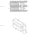
- FIG. 1A is a sectional view of the essential portion of the multilayer dielectric line circuit.
- Fig. 1B is a partial perspective view of the essential portion thereof, in which the illustration of three conductor plates is omitted.
- reference numerals 1, 2, and 3 each denote a conductor plate, with two parallel conductor planes being formed by the conductor plates 1 and 2, and another two parallel conductor planes being formed by the conductor plates 2 and 3.
- Fig. 1A reference numerals 1, 2, and 3 each denote a conductor plate, with two parallel conductor planes being formed by the conductor plates 1 and 2, and another two parallel conductor planes being formed by the conductor plates 2 and 3.
- a dielectric strip 4 and a cylindrical dielectric resonator 6 are disposed between the conductor plates 1 and 2, and a dielectric strip 5 and a cylindrical dielectric resonator 7 are disposed between the conductor plates 2 and 3.
- a circular opening portion 12 is formed at the portion sandwiched by the dielectric resonators 6 and 7.
- the conductor plates 1 and 2 and the dielectric strip 4 form a dielectric line in a lower layer, and the conductor plates 2 and 3 and the dielectric strip 5 form a dielectric line in an upper layer.
- the spacing between the conductor plates 1 and 2 and the spacing between the conductor plates 3 and 3 are set to a half-wave length or less of the propagation wavelength in the free space, and each dielectric strip is disposed between each pair of conductor plates, thus each functions as a nonradiative dielectric line (NRD guide).
- the dielectric resonators 6 and 7 are a TE011-mode or HE111- mode dielectric resonator, and the dielectric strips 4 and 5 are magnetically connected to the dielectric resonators 6 and 7, respectively. Also, the dielectric resonators 6 and 7 are magnetically connected to each other.
- Fig. 2 is an equivalent circuit diagram of the multilayer dielectric line circuit shown in Fig. 1.
- reference numerals 4' and 5' denote two dielectric lines formed by the dielectric strips 4 and 5 and the conductor plates 1, 2 and 3 shown in Fig. 1.
- Reference numerals 6' and 7' denote two dielectric resonators formed by the dielectric strips 6 and 7 and the conductor plates 1, 2 and 3 shown in Fig. 1.
- the dielectric line 4' is magnetically connected to the dielectric resonator 6'
- the dielectric resonator 6' is magnetically connected to the dielectric resonator 7'
- the dielectric resonator 7' is magnetically connected to the dielectric line 5'
- the dielectric line 4' of the lower layer is eventually connected to the dielectric line 5' of the upper layer via a band-pass filter of two stages. Therefore, a frequency signal of the passing band of this band-pass filter can be transmitted between ports #1 and #2 shown in Fig. 2.
- Frequency signals of other than the passing band are attenuated or cut off between ports #1 and #2.
- a pass band or a cut-off band having this band passing characteristic may be used as required.
- FIGS. 3A and 3B show examples of a modification of the multilayer dielectric line circuit shown in Fig. 1.
- Figs. 3A and 3B show in the plan views the positional relationship of a dielectric strip and a dielectric resonator in an upper layer and the positional relationship between a dielectric strip and a dielectric resonator in a lower layer each with the positions being shifted up and down in the figure.
- the dielectric resonators 6 and 7 are disposed coaxially similar to the case shown in Fig. 1, and further, whereas the angle formed by the dielectric strips 4 and 5 is set to 01 ⁇ 2 in the example shown in Fig. 1, in Figs. 3A and 3B, a predetermined angle is provided.
- the electromagnetic waves of the LMS01 mode which propagate through the dielectric strip 4 are propagated as the electromagnetic waves of the LMS01 mode similarly through the dielectric strip 5 via the dielectric resonators 6 and 7.
- the dielectric resonators 6 and 7 of the HE111 mode are used.
- the space between the dielectric strip and the dielectric resonator 6 is magnetically connected, and the space between the dielectric resonator 7 and the dielectric resonator 6 is magnetically connected.
- the electromagnetic-field distribution of the dielectric resonators 6 and 7 is rotationally symmetric about the axis and can be determined as desired, its use for conversion in the transmission direction is also possible.
- Figs. 4A, 4B and Fig. 5 show the construction of a multilayer dielectric line circuit according to a second embodiment of the present invention.
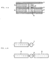
- Fig. 4A is a sectional view of the essential portion of the multilayer dielectric line circuit.
- Fig. 4B is a sectional view of the essential portion of the multilayer dielectric line circuit.
- FIG. 4B shows in the plan views the positional relationship between a dielectric strip and a dielectric resonator in the lower layer and the positional relationship between a dielectric strip and a dielectric resonator in a upper layer with the positions shifted up and down in the figure.
- two dielectric strips 4 and 8 which connect to the dielectric resonator 6 in the lower layer are provided in the lower layer portion.
- the other construction is the same as the construction shown in Fig. 1.
- Fig. 5 is an equivalent circuit diagram of the circuit shown in Fig. 4.
- Reference numerals 4', 5' and 8' denote dielectric lines formed by the dielectric strips 4, 5 and 8, respectively, shown in Fig. 4.
- Reference numerals 6' and 7' denote resonators formed by the dielectric resonators 6 and 7 and the conductor plates 1, 2 and 3 shown in Fig. 4.
- the dielectric strips 4 and 8 are each magnetically connected to the dielectric resonator 6, the dielectric resonator 6 is magnetically connected to the dielectric resonator 7, and the dielectric resonator 7 is magnetically connected to the dielectric strip 5, with the result being that the signal, for example, input from port #1, is output to each of ports #2 and #3.
- Figs. 6A and 6B show the construction of a multilayer dielectric line circuit according to a third embodiment of the present invention.
- Fig. 6A is a sectional view of the essential portion thereof.
- 6B shows in the plan views the positional relationship between a dielectric strip and a dielectric resonator in an upper layer and the positional relationship between a dielectric strip and a dielectric resonator in a lower layer with the positions shifted up and down in the figure.
- the dielectric resonator 9 is disposed between the dielectric resonator 6 and the dielectric strip 4 for performing interlayer connection
- the dielectric resonator 10 is disposed between the dielectric resonator 7 and the dielectric strip 5 for performing interlayer connection, with the result being that this becomes equivalent to the following: a band-pass filter formed by a four-stage dielectric resonator is provided between the dielectric line in the lower layer formed by the conductor plates 1 and 2 and the dielectric strip 4, and the dielectric line in the upper layer formed by the conductor plates 2 and 3 and the dielectric strip 5.
- formation of a resonator into multiple stages makes it possible to achieve a wider band. Figs.
- Fig. 7A and 7B show the construction of a multilayer dielectric line circuit according to a fourth embodiment of the present invention.
- Fig. 7A is a sectional view of the essential portion thereof.
- Fig. 7B shows the positional relationship and the connection relationship between a dielectric strip and a dielectric resonator.
- a dielectric strip 4 and a dielectric resonator 6 are provided between conductor plates 1 and 2
- a dielectric strip 5 and a dielectric resonator 7 are provided between conductor plates 2 and 3.
- the dielectric resonators 6 and 7 are coaxially disposed, and the dielectric strips 4 and 5 are disposed in a positional relationship spaced apart by a fixed distance on the sides of the dielectric resonators 6 and 7, respectively.
- the LMS-mode electromagnetic waves which propagate through the dielectric strips 4 and 5 are electrically connected respectively to the dielectric resonators 6 and 7 of the TE011 mode. Further, the space between the upper and lower dielectric resonators 6 and 7 is magnetically connected. Whether the space between the dielectric strip and the dielectric resonator is magnetically connected or electrically connected can be selected as desired.
- the space between the dielectric strip 4 and the dielectric resonator 6 in the lower layer may be magnetically connected similar to the first to third embodiments, and the space between the dielectric strip 5 and the dielectric resonator 7 in the upper layer may be electrically connected, or conversely, the lower layer may be electrically connected and the upper layer may be magnetically connected.
- a dielectric resonator for interlayer connection is sandwiched between two conductor planes, as shown in the sectional views in Fig. 8, a dielectric resonator may be supported by either one of the upper and lower conductor plates. In the example shown in Fig.
- dielectric resonators 6 and 7 are bonded to the inner surfaces of the conductor plates 1 and 3, respectively.
- the dielectric resonators 6 and 7 are fixed to the inner surfaces of the conductor plates 1 and 3, respectively, via support bases having a low dielectric constant, the dielectric resonator 6 is disposed at nearly the middle position of the conductor plates 1 and 2, and the dielectric resonator 7 is disposed at nearly the middle position of the conductor plates 2 and 3.
- the dielectric resonators 6 and 7 are each excited in the TE01 mode.
- Figs. 9A, 9B and 9C show examples of various shapes of an opening portion provided in the conductor plate 2 in each of the above-described embodiments. As shown in Fig. 9A, a circular hole is provided, or as shown in Fig. 9B, a square hole is provided, and the degree of connection between upper and lower dielectric resonators is set according to the areas of these openings. Further, as shown in Fig. 9A, a circular hole is provided, or as shown in Fig. 9B, a square hole is provided, and the degree of connection between upper and lower dielectric resonators is set according to the areas of these openings. Further, as shown in Fig.
- slit-shaped opening portions 12 are provided, and the degree of connection is set according to the width and length of the slits.
- a simple opening portion 12 is provided in the conductor plate 2
- a substrate 13 for connection adjustment is provided in one or both of the facing surfaces of dielectric resonators 6 and 7, and the degree of connection may be set according to an electrode pattern on the substrate.
- Fig. 10B shows an electrode pattern of the substrate 13, in which the hatched portion is an electrode, and the portion indicated by reference numeral 14 is a circular ring slot with no electrode. The degree of connection is set according to the diameter and width of this circular ring slot.
- FIG. 11A and 11B are sectional views of a multilayer dielectric line circuit according to a fifth embodiment of the present invention.
- Fig. 12 is an equivalent circuit diagram of the multilayer dielectric line circuit according to the fifth embodiment of the present invention.
- one dielectric resonator 11 is disposed near the end surface of each of a dielectric strip 4 in the lower layer and a dielectric strip 5 in the upper layer and at nearly the middle position of the upper and lower layers.
- a gap of each of the conductor plates 1, 2 and 3 is filled with a resin having a low dielectric constant, and the dielectric resonator 11 is fixed by the resin.
- Fig. 11A one dielectric resonator 11 is disposed near the end surface of each of a dielectric strip 4 in the lower layer and a dielectric strip 5 in the upper layer and at nearly the middle position of the upper and lower layers.
- a gap of each of the conductor plates 1, 2 and 3 is filled with a resin having a low dielectric constant, and the dielectric re
- a dielectric resonator 11 is disposed between the conductor plates 1 and 3 in such a manner as to go through the opening portion 12 provided in the conductor plate 2.
- the equivalent circuit becomes as shown in Fig. 12, the dielectric strips 4 and 5 are each magnetically connected to the dielectric resonator 11, and thus the dielectric line in the lower layer and the dielectric line in the upper layer are connected to each other via a one-stage resonator (a band-pass filter).
- Figs. 13A, 13B and 13C show an example of the application of the dielectric line circuit to a front-end apparatus for a millimetric-wave radar according to a sixth embodiment of the present invention.
- FIG. 13A shows a dielectric line circuit in an upper layer.
- Fig. 13B shows a dielectric line circuit in a lower layer.
- Fig. 13C is a sectional view of a front-end apparatus for a millimetric-wave radar, formed by assembling these two dielectric line circuits into a case.
- a dielectric line circuit 50 in the lower layer is formed with an oscillator 32, an interlayer connector 26, a primary vertical radiator 20, and a circuit block 22.
- the illustration of an upper conductor plate is omitted.
- the oscillator 32 is formed with an oscillation circuit formed of a Gunn diode and the like, and an oscillation signal therefrom is transmitted to the primary vertical radiator 20 via a dielectric strip 33, a circulator 28, and a dielectric strip 29.
- a terminater 31 is provided at the terminal end of a dielectric strip 30, which is one port of the circulator 28.
- a terminater 25 is provided in one of the end portions of a dielectric strip 24, and the other end portion is connected to the interlayer connector 26.
- the proximity portion of the dielectric strips 29 and 24 is formed as a coupler 23.
- the primary vertical radiator 20 is provided with a dielectric resonator 21, and this is excited in the HE111 mode in order to radiate linearly polarized electromagnetic waves in a direction vertical to the paper surface. Meanwhile, the transmission signal is supplied to the interlayer connector 26 via the coupler 23 and the dielectric strip 24.
- a dielectric resonator 27 provided in the interlayer connector 26 is disposed coaxially with the dielectric resonator provided in the interlayer connector of the dielectric line circuit in the upper layer.
- a dielectric line circuit 51 in the upper layer is provided with a primary vertical radiator 40, an interlayer connector 34, and a mixer 36.
- the interlayer connectors 26 and 34 overlap in the relationship in which the dielectric resonators 27 and 35 are coaxial.
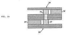
- FIG. 14 The sectional view of this interlayer connector portion is shown in Fig. 14.
- an opening portion is provided in each of the lower conductor plate of the interlayer connector 34 in the upper layer and the upper conductor plate of the interlayer connector 26 in the lower layer, and the upper and lower two dielectric resonators 35 and 27 are disposed to face each other in an axial direction via this opening portion.
- the dielectric resonator 27 in the lower layer and the dielectric resonator 35 in the upper layer are magnetically connected to each other. Therefore, the above-described oscillation signal shown in Fig. 13 is supplied as a local signal Lo to the mixer 36.
- the waves reflected from an object excite a dielectric resonator 41 of the primary vertical radiator 40, and the received signal (RF signal) is input to the other port of the mixer 36.
- the two signals are mixed by a coupler 37 and output to the two ports with a phase difference of 901 ⁇ 2.
- a mixer circuit formed of a Schottky barrier diode and the like is formed in the two ports.
- dielectric lenses 52 and 53 are disposed in front of the dielectric resonators 21 and 41 of the primary vertical radiator, respectively.
- Fig. 15A and 15B show the construction of a front- end apparatus for a millimetric-wave radar according to a seventh embodiment of the present invention.
- Fig. 15A is a top plan view thereof.
- Fig. 15B is a front view thereof.
- the dielectric line circuit 50 in the lower layer and the dielectric line circuit 51 in the upper layer are laminated nearly similar to the example shown in Figs. 13A, 13B and 13C.
- a primary vertical radiator is not used, dielectric rods 55 and 56 are each made to protrude from between conductor plates, and electromagnetic waves are transmitted or received in the direction of the propagation of electromagnetic waves through the dielectric line.
- the dielectric lenses 52 and 53 are disposed parallel to the upper and lower surfaces of the case, and further, a smaller size is achieved as a whole.
- a dielectric line into a multilayer, the entire area is reduced, and further, interlayer connection is performed without using a hollow waveguide, and no wasteful interlayer space occurs; thus, a smaller size is achieved as a whole.
- a multi-branching circuit having, for example, three or more ports can be easily formed within a limited space.
- the degree of connection between dielectric resonators for interlayer connection can be easily set and adjusted. Further, according to the present invention of claim 5, since connection among different layers is made via dielectric resonators of multiple stages, a wider band of a connection frequency band can be achieved.
- Many different embodiments of the present invention may be constructed without departing from the spirit and scope of the present invention. It should be understood that the present invention is not limited to the specific embodiments described in this specification. To the contrary, the present invention is intended to cover various modifications and equivalent arrangements included within the spirit and scope of the invention as hereafter claimed. The scope of the following claims is to be accorded the broadest interpretation so as to encompass all such modifications, equivalent structures and functions.
Landscapes
- Control Of Motors That Do Not Use Commutators (AREA)
- Waveguides (AREA)
Applications Claiming Priority (3)
| Application Number | Priority Date | Filing Date | Title |
|---|---|---|---|
| JP190844/96 | 1996-07-19 | ||
| JP08190844A JP3134781B2 (ja) | 1996-07-19 | 1996-07-19 | 多層誘電体線路回路 |
| JP19084496 | 1996-07-19 |
Publications (2)
| Publication Number | Publication Date |
|---|---|
| EP0820114A1 true EP0820114A1 (fr) | 1998-01-21 |
| EP0820114B1 EP0820114B1 (fr) | 2002-10-16 |
Family
ID=16264719
Family Applications (1)
| Application Number | Title | Priority Date | Filing Date |
|---|---|---|---|
| EP97111554A Expired - Lifetime EP0820114B1 (fr) | 1996-07-19 | 1997-07-08 | Circuit de ligne diélectrique multicouches |
Country Status (4)
| Country | Link |
|---|---|
| US (1) | US5943005A (fr) |
| EP (1) | EP0820114B1 (fr) |
| JP (1) | JP3134781B2 (fr) |
| DE (1) | DE69716359T2 (fr) |
Cited By (1)
| Publication number | Priority date | Publication date | Assignee | Title |
|---|---|---|---|---|
| EP0855755A3 (fr) * | 1997-01-23 | 2000-05-31 | Murata Manufacturing Co., Ltd. | Croisement pour lignes diélectriques |
Families Citing this family (23)
| Publication number | Priority date | Publication date | Assignee | Title |
|---|---|---|---|---|
| JP3316561B2 (ja) * | 1998-07-06 | 2002-08-19 | 株式会社村田製作所 | アレーアンテナ装置および無線装置 |
| JP3735510B2 (ja) * | 2000-04-18 | 2006-01-18 | 株式会社村田製作所 | 伝送線路接続構造、高周波モジュールおよび通信装置 |
| JP2003101301A (ja) * | 2001-09-19 | 2003-04-04 | Murata Mfg Co Ltd | 高周波モジュール、通信装置およびレーダ装置 |
| JP3862633B2 (ja) * | 2002-08-14 | 2006-12-27 | 東京エレクトロン株式会社 | 非放射性誘電体線路の製造方法 |
| US7420436B2 (en) * | 2006-03-14 | 2008-09-02 | Northrop Grumman Corporation | Transmission line to waveguide transition having a widened transmission with a window at the widened end |
| US7714776B2 (en) * | 2006-06-27 | 2010-05-11 | National University Of Ireland Maynooth | Antenna array calibration |
| US7733265B2 (en) * | 2008-04-04 | 2010-06-08 | Toyota Motor Engineering & Manufacturing North America, Inc. | Three dimensional integrated automotive radars and methods of manufacturing the same |
| US7830301B2 (en) * | 2008-04-04 | 2010-11-09 | Toyota Motor Engineering & Manufacturing North America, Inc. | Dual-band antenna array and RF front-end for automotive radars |
| US8022861B2 (en) * | 2008-04-04 | 2011-09-20 | Toyota Motor Engineering & Manufacturing North America, Inc. | Dual-band antenna array and RF front-end for mm-wave imager and radar |
| US7990237B2 (en) * | 2009-01-16 | 2011-08-02 | Toyota Motor Engineering & Manufacturing North America, Inc. | System and method for improving performance of coplanar waveguide bends at mm-wave frequencies |
| US8786496B2 (en) | 2010-07-28 | 2014-07-22 | Toyota Motor Engineering & Manufacturing North America, Inc. | Three-dimensional array antenna on a substrate with enhanced backlobe suppression for mm-wave automotive applications |
| US10411320B2 (en) | 2015-04-21 | 2019-09-10 | 3M Innovative Properties Company | Communication devices and systems with coupling device and waveguide |
| CN107534199B (zh) * | 2015-04-21 | 2022-06-17 | 3M创新有限公司 | 具有高电介质谐振器的波导 |
| EP3286798B1 (fr) * | 2015-04-21 | 2022-06-01 | 3M Innovative Properties Company | Dispositifs et systèmes de communication avec dispositif de couplage et guide d'ondes |
| US11283189B2 (en) | 2017-05-02 | 2022-03-22 | Rogers Corporation | Connected dielectric resonator antenna array and method of making the same |
| KR102312067B1 (ko) * | 2017-06-07 | 2021-10-13 | 로저스코포레이션 | 유전체 공진기 안테나 시스템 |
| US11616302B2 (en) | 2018-01-15 | 2023-03-28 | Rogers Corporation | Dielectric resonator antenna having first and second dielectric portions |
| US11552390B2 (en) | 2018-09-11 | 2023-01-10 | Rogers Corporation | Dielectric resonator antenna system |
| JP2022510892A (ja) | 2018-12-04 | 2022-01-28 | ロジャーズ コーポレーション | 誘電体電磁構造およびその製造方法 |
| US20210096209A1 (en) * | 2019-09-26 | 2021-04-01 | Rogers Corporation | Radar-enabled multi-vehicle system |
| CN111446526B (zh) * | 2020-03-27 | 2021-11-02 | 广东国华新材料科技股份有限公司 | 一种介质滤波器 |
| US11482790B2 (en) | 2020-04-08 | 2022-10-25 | Rogers Corporation | Dielectric lens and electromagnetic device with same |
| US11670828B1 (en) | 2021-04-27 | 2023-06-06 | Rockwell Collins, Inc. | Dielectric and thin film floating metal stacking for embedded tunable filtering of high frequency signals |
Family Cites Families (6)
| Publication number | Priority date | Publication date | Assignee | Title |
|---|---|---|---|---|
| JP2552520B2 (ja) * | 1988-02-22 | 1996-11-13 | 関商事株式会社 | Nrdガイドフィルタ |
| JP3123293B2 (ja) * | 1993-03-05 | 2001-01-09 | 株式会社村田製作所 | 非放射性誘電体線路およびその製造方法 |
| EP0618642B1 (fr) * | 1993-03-31 | 2001-09-19 | Hitachi Kokusai Electric Inc. | Radiateur électromagnétique pour radiation et réception d ondes électromagnétiques |
| JP3042364B2 (ja) * | 1995-05-19 | 2000-05-15 | 株式会社村田製作所 | 誘電体アンテナ |
| JP3045046B2 (ja) * | 1995-07-05 | 2000-05-22 | 株式会社村田製作所 | 非放射性誘電体線路装置 |
| JP5550602B2 (ja) | 2011-04-28 | 2014-07-16 | パナソニック株式会社 | 静電チャックおよびこれを備えるドライエッチング装置 |
-
1996
- 1996-07-19 JP JP08190844A patent/JP3134781B2/ja not_active Expired - Fee Related
-
1997
- 1997-07-08 DE DE69716359T patent/DE69716359T2/de not_active Expired - Fee Related
- 1997-07-08 EP EP97111554A patent/EP0820114B1/fr not_active Expired - Lifetime
- 1997-07-18 US US08/897,250 patent/US5943005A/en not_active Expired - Fee Related
Non-Patent Citations (5)
| Title |
|---|
| AMR ABDELMONEM ET AL: "FULL-WAVE DESIGN OF SPURIOUS FREE D.R. TE MODE BAND PASS FILTERS", IEEE TRANSACTIONS ON MICROWAVE THEORY AND TECHNIQUES, vol. 43, no. 4, PART 01, 1 April 1995 (1995-04-01), pages 744 - 752, XP000496278 * |
| I.J. BAHL ET AL.: "APERTURE COUPLING BETWEEN DIELECTRIC IMAGE LINES", IEEE TRANSACTIONS ON MICROWAVE THEORY AND TECHNIQUES., vol. 29, no. 9, September 1981 (1981-09-01), NEW YORK US, pages 891 - 896, XP002044397 * |
| ISHIKAWA Y ET AL: "PLANAR TYPE DIELECTRIC RESONATOR FILTER AT MILLIMETER-WAVE FREQUENCY", IEICE TRANSACTIONS ON ELECTRONICS, vol. E79-C, no. 5, 1 May 1996 (1996-05-01), pages 679 - 684, XP000621611 * |
| NALLO DI C ET AL: "EXPERIMENTAL INVESTIGATION ON NRD-GUIDE DUAL-MODE FILTERS", IEEE MTT-S INTERNATIONAL MICROWAVE SYMPOSIUM DIGEST, SAN DIEGO, MAY 23 - 27, 1994, vol. 1, 23 May 1994 (1994-05-23), KUNO H J;WEN C P (EDITORS), pages 237 - 240, XP000527278 * |
| XU S ET AL: "SCATTERING PROPERTIES OF DISCONTINUITIES IN NRD GUIDE", IEE PROCEEDINGS: MICROWAVES, ANTENNAS AND PROPAGATION, vol. 141, no. 3, PART H, 1 June 1994 (1994-06-01), pages 205 - 210, XP000459827 * |
Cited By (1)
| Publication number | Priority date | Publication date | Assignee | Title |
|---|---|---|---|---|
| EP0855755A3 (fr) * | 1997-01-23 | 2000-05-31 | Murata Manufacturing Co., Ltd. | Croisement pour lignes diélectriques |
Also Published As
| Publication number | Publication date |
|---|---|
| DE69716359D1 (de) | 2002-11-21 |
| JPH1041712A (ja) | 1998-02-13 |
| JP3134781B2 (ja) | 2001-02-13 |
| DE69716359T2 (de) | 2003-09-11 |
| US5943005A (en) | 1999-08-24 |
| EP0820114B1 (fr) | 2002-10-16 |
Similar Documents
| Publication | Publication Date | Title |
|---|---|---|
| EP0820114B1 (fr) | Circuit de ligne diélectrique multicouches | |
| US6052087A (en) | Antenna device and radar module | |
| EP0896380B1 (fr) | Guide d'ondes diélectrique | |
| JP3891918B2 (ja) | 高周波モジュール | |
| JP3163981B2 (ja) | 送受信装置 | |
| EP1263078B1 (fr) | Ligne de transmission, circuit intégré et émetteur-récepteur | |
| EP1396903A2 (fr) | Guide d' onde diélectrique et son dispositif de branchement | |
| US6144267A (en) | Non-Radiative dielectric line assembly | |
| CA2256283C (fr) | Guide d'ondes dielectrique non radiatif comprenant une partie pour la conversion de ligne entre differents types de guides d'ondes dielectriques non radiatifs | |
| JP3013798B2 (ja) | 交差線路 | |
| Yoneyama | Millimeter‐wave integrated circuits using nonradiative dielectric waveguide | |
| KR100519424B1 (ko) | 선로 결합 구조, 믹서 및 송수신 장치 | |
| US6496080B1 (en) | Dielectric waveguide nonreciprocal circuit device with a non-interfering magnetic member support | |
| US6359526B1 (en) | Nonreciprocal circuit device including dielectric wave guide and a lower dielectric constant medium | |
| JP3259637B2 (ja) | 送受信装置 | |
| EP0957528A1 (fr) | Dispositif de circuit non réciproque avec guide d' ondes diélectrique, dispositif de guide d' ondes diélectrique et appareil radio | |
| JP2002237705A (ja) | 非放射性誘電体線路、高周波回路部品および高周波回路モジュール |
Legal Events
| Date | Code | Title | Description |
|---|---|---|---|
| PUAI | Public reference made under article 153(3) epc to a published international application that has entered the european phase |
Free format text: ORIGINAL CODE: 0009012 |
|
| 17P | Request for examination filed |
Effective date: 19970708 |
|
| AK | Designated contracting states |
Kind code of ref document: A1 Designated state(s): DE FR GB |
|
| AKX | Designation fees paid |
Free format text: DE FR GB |
|
| RBV | Designated contracting states (corrected) |
Designated state(s): DE FR GB |
|
| 17Q | First examination report despatched |
Effective date: 20000626 |
|
| GRAG | Despatch of communication of intention to grant |
Free format text: ORIGINAL CODE: EPIDOS AGRA |
|
| GRAG | Despatch of communication of intention to grant |
Free format text: ORIGINAL CODE: EPIDOS AGRA |
|
| GRAH | Despatch of communication of intention to grant a patent |
Free format text: ORIGINAL CODE: EPIDOS IGRA |
|
| GRAH | Despatch of communication of intention to grant a patent |
Free format text: ORIGINAL CODE: EPIDOS IGRA |
|
| GRAA | (expected) grant |
Free format text: ORIGINAL CODE: 0009210 |
|
| AK | Designated contracting states |
Kind code of ref document: B1 Designated state(s): DE FR GB |
|
| REG | Reference to a national code |
Ref country code: GB Ref legal event code: FG4D |
|
| REF | Corresponds to: |
Ref document number: 69716359 Country of ref document: DE Date of ref document: 20021121 |
|
| ET | Fr: translation filed | ||
| PLBE | No opposition filed within time limit |
Free format text: ORIGINAL CODE: 0009261 |
|
| STAA | Information on the status of an ep patent application or granted ep patent |
Free format text: STATUS: NO OPPOSITION FILED WITHIN TIME LIMIT |
|
| 26N | No opposition filed |
Effective date: 20030717 |
|
| PGFP | Annual fee paid to national office [announced via postgrant information from national office to epo] |
Ref country code: DE Payment date: 20080717 Year of fee payment: 12 |
|
| PGFP | Annual fee paid to national office [announced via postgrant information from national office to epo] |
Ref country code: FR Payment date: 20080718 Year of fee payment: 12 |
|
| PGFP | Annual fee paid to national office [announced via postgrant information from national office to epo] |
Ref country code: GB Payment date: 20080709 Year of fee payment: 12 |
|
| GBPC | Gb: european patent ceased through non-payment of renewal fee |
Effective date: 20090708 |
|
| REG | Reference to a national code |
Ref country code: FR Ref legal event code: ST Effective date: 20100331 |
|
| PG25 | Lapsed in a contracting state [announced via postgrant information from national office to epo] |
Ref country code: FR Free format text: LAPSE BECAUSE OF NON-PAYMENT OF DUE FEES Effective date: 20090731 |
|
| PG25 | Lapsed in a contracting state [announced via postgrant information from national office to epo] |
Ref country code: GB Free format text: LAPSE BECAUSE OF NON-PAYMENT OF DUE FEES Effective date: 20090708 |
|
| PG25 | Lapsed in a contracting state [announced via postgrant information from national office to epo] |
Ref country code: DE Free format text: LAPSE BECAUSE OF NON-PAYMENT OF DUE FEES Effective date: 20100202 |