EP0820154A2 - Radio émetteur-récepteur à deux bandes - Google Patents
Radio émetteur-récepteur à deux bandes Download PDFInfo
- Publication number
- EP0820154A2 EP0820154A2 EP97660082A EP97660082A EP0820154A2 EP 0820154 A2 EP0820154 A2 EP 0820154A2 EP 97660082 A EP97660082 A EP 97660082A EP 97660082 A EP97660082 A EP 97660082A EP 0820154 A2 EP0820154 A2 EP 0820154A2
- Authority
- EP
- European Patent Office
- Prior art keywords
- filter means
- signal
- amplifier
- frequency band
- filter
- Prior art date
- Legal status (The legal status is an assumption and is not a legal conclusion. Google has not performed a legal analysis and makes no representation as to the accuracy of the status listed.)
- Granted
Links
- 238000004891 communication Methods 0.000 claims abstract description 40
- 238000001914 filtration Methods 0.000 claims abstract description 21
- 230000005540 biological transmission Effects 0.000 claims description 24
- 238000000034 method Methods 0.000 description 5
- 238000010295 mobile communication Methods 0.000 description 3
- 238000010586 diagram Methods 0.000 description 2
- 230000009977 dual effect Effects 0.000 description 2
- 238000001228 spectrum Methods 0.000 description 2
- 230000001360 synchronised effect Effects 0.000 description 2
- IRLPACMLTUPBCL-KQYNXXCUSA-N 5'-adenylyl sulfate Chemical compound C1=NC=2C(N)=NC=NC=2N1[C@@H]1O[C@H](COP(O)(=O)OS(O)(=O)=O)[C@@H](O)[C@H]1O IRLPACMLTUPBCL-KQYNXXCUSA-N 0.000 description 1
- 230000015572 biosynthetic process Effects 0.000 description 1
- 230000000903 blocking effect Effects 0.000 description 1
- 230000008878 coupling Effects 0.000 description 1
- 238000010168 coupling process Methods 0.000 description 1
- 238000005859 coupling reaction Methods 0.000 description 1
- 230000001419 dependent effect Effects 0.000 description 1
- 238000004519 manufacturing process Methods 0.000 description 1
- 238000009738 saturating Methods 0.000 description 1
- 230000008054 signal transmission Effects 0.000 description 1
Images


Classifications
-
- H—ELECTRICITY
- H04—ELECTRIC COMMUNICATION TECHNIQUE
- H04B—TRANSMISSION
- H04B1/00—Details of transmission systems, not covered by a single one of groups H04B3/00 - H04B13/00; Details of transmission systems not characterised by the medium used for transmission
- H04B1/38—Transceivers, i.e. devices in which transmitter and receiver form a structural unit and in which at least one part is used for functions of transmitting and receiving
- H04B1/40—Circuits
- H04B1/50—Circuits using different frequencies for the two directions of communication
- H04B1/52—Hybrid arrangements, i.e. arrangements for transition from single-path two-direction transmission to single-direction transmission on each of two paths or vice versa
- H04B1/525—Hybrid arrangements, i.e. arrangements for transition from single-path two-direction transmission to single-direction transmission on each of two paths or vice versa with means for reducing leakage of transmitter signal into the receiver
-
- H—ELECTRICITY
- H04—ELECTRIC COMMUNICATION TECHNIQUE
- H04B—TRANSMISSION
- H04B1/00—Details of transmission systems, not covered by a single one of groups H04B3/00 - H04B13/00; Details of transmission systems not characterised by the medium used for transmission
- H04B1/38—Transceivers, i.e. devices in which transmitter and receiver form a structural unit and in which at least one part is used for functions of transmitting and receiving
- H04B1/40—Circuits
- H04B1/403—Circuits using the same oscillator for generating both the transmitter frequency and the receiver local oscillator frequency
- H04B1/406—Circuits using the same oscillator for generating both the transmitter frequency and the receiver local oscillator frequency with more than one transmission mode, e.g. analog and digital modes
-
- H—ELECTRICITY
- H04—ELECTRIC COMMUNICATION TECHNIQUE
- H04B—TRANSMISSION
- H04B1/00—Details of transmission systems, not covered by a single one of groups H04B3/00 - H04B13/00; Details of transmission systems not characterised by the medium used for transmission
- H04B1/38—Transceivers, i.e. devices in which transmitter and receiver form a structural unit and in which at least one part is used for functions of transmitting and receiving
- H04B1/40—Circuits
- H04B1/54—Circuits using the same frequency for two directions of communication
- H04B1/56—Circuits using the same frequency for two directions of communication with provision for simultaneous communication in two directions
Definitions
- the present invention relates to an arrangement for transmitting radio frequency signal, i.e. RF signal, at two different transmitting frequency bands and for receiving at two different reception frequency bands.
- the arrangement is applicable, among others, in a transceiver of a radio communications system operating at two frequency bands or in a transceiver meant to be used in connection with two radio communications systems.
- FIG. 1 is a block diagram of the radio frequency parts, i.e. RF parts, of a prior art multi-mode mobile telephone operating at two different frequency bands.
- RF parts radio frequency parts
- the system includes a separate RF front end for both frequency bands as well as for the receiver and the transmitter respectively; in the receiver part, this RF front end comprises a pre-amplifier 2, 27 and an RF filter 3, 28, and in the transmitter part filters 19, 23 and a power amplifier 18, 24 as well as duplex filters 1, 25 for both frequency bands.
- two-way switches 26, 29, 31 are provided in the antenna front end and at the antenna-side ports of the mixers of the receiver and transmitter. While operating at two different frequency bands, two duplex filters 1, 25, two preamplifiers 2, 27 and two RF filters 3, 28 are employed in the signal reception. Respectively, in signal transmission, there are used two RF filters 19, 23 of the transmitter, two power amplifiers 18, 24 and two duplex filters 1, 25. By means of the two-way switches 26, 29, 31, one of the two blocks of the same type are always in use. In order to create two different first mixer frequencies LO1, in the synthesiser S1 there are provided two voltage controlled means of the two-way switches 26, 29, 31, one of the two blocks of the same type are always in use.
- the synthesiser S1 there are provided two voltage controlled oscillators 13, 30, one of which is switched to be active by the controls V1 and V2, depending on the respective frequency band of operation, for instance the frequency band of the GSM or the PCN system.
- the employed controls V1 and V2 can be the oscillator operating voltages (i.e. one is switched to operating voltage, the other is not).
- Each oscillator 13, 30 gives a different output frequency.
- the phase-locked loop 15 whereof includes two different frequency dividers, one of which is always eligible for use.
- the division number of the divider 22 is chosen by the control NX.
- the division number for the PCN system is 2 and for the GSM system 1.
- the signal first passes through a first intermediate frequency filter 5 to a second mixer 6, where it is mixed with the second mixer frequency LO2 in order to create a second intermediate frequency IF2.
- the signal passes through a second intermediate frequency filter 8 and through +45° and -45° phase transfer blocks 10 and 11 to a demodulator 12, advantageously to an I/Q demodulator, where the local oscillator frequency LO3 also is brought.
- the signal I-TX, Q-TX entering a modulator in order to be transmitted is taken from the modulator 21, advantageously an I/Q modulator - where in addition to the signal to be transmitted, there also is brought as the modulator carrier wave signal, the frequency of the second mixer frequency LO2 divided by the divider 22 - into a mixer 20; in said mixer 20, the signal is mixed to transmitting frequency FTX with the first mixer frequency LO1. From the mixer 20, the signal is brought through a transmitter-frequency RF filter 19 to a power amplifier 18, wherefrom the amplified signal is brought via the duplex filter 1 to the antenna ANT.
- GSM reception: 935,2...959,8 MHz transmission: 890...915 MHz
- PCN reception: 1805,2...1879,8 MHz transmission: 1710,2...1784,8 MHz mixer frequency LO1: 1524,8...1599,4 MHz (RX) 1544,0...1618,6 MHz (TX)
- a drawback of the prior art solution according to figure 1 is that for its RF interface, there is needed a remarkable number of filters (1, 3, 19, 23, 25, 28) and controllable switches (26, 29, 31) on the signal path, which makes the RF front end complicated and increases production expenses. Moreover, the switches cause attenuation on the signal path in the conducting mode, and "leak", i.e. pass signals also in the open state.
- the object of the present invention is to create an arrangement whereby the above described drawbacks of the prior art can be avoided.
- One of the ideas of the invention is that one and the same filter belonging to the RF front end is used for filtering interference from two different signals, in which case the number of filters can be reduced.
- the number of controllable switches required on the signal path of the RF front end can likewise be minimised.
- a synchronised switch in a telephone of a time division system, so that in the receiving mode, the switch directs the signal from the antenna to the receiver and blocks the signal path from the transmitter to the antenna. In the transmitting mode, the switch leads the signal from the transmitter to the antenna and blocks the signal path from the antenna to the receiver.
- a main idea of the present invention is that one and the same synchronised switch can be used, in addition to time divided transmission and reception selection, also in the selection of the frequency band in multi-mode mobile telephones or in the so-called third-generation systems that apply dual mode operation. Thus the need for additional switches can be avoided.
- the system according to the invention for transmitting and receiving RF signal in which transmitting can take place in the first and in the second transmitter frequency band, said first and second transmitter frequency bands being separate, and where the reception can take place at the first and at the second receiver frequency band, said first and second receiver frequency bands being separate.
- the arrangement comprises filtering means for filtering the received and transmitted signal, is characterised in that at least one filtering means is used for filtering signals in at least two different frequency bands.
- the signal received at the first receiver frequency band or band will be called the first signal
- the signal received at the second receiver frequency band will be called the second signal
- the signal to be transmitted at the first transmitter frequency band will be called the third signal
- the signal to be transmitted at the second transmitter frequency band will be called the fourth signal. Said terms will be used irrespective of the location of said signals in the transmission or reception chain.
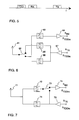
- Figure 2 illustrates frequency bands used by a communication system on a frequency axis f, where the frequency is illustrated as growing from left to right.
- TX for transmission and RX for reception
- TDD which is used for both transmission and reception.
- This type of communication system can be for instance UMTS.
- the distance of the first transmission frequency (TX) from the second transmission frequency band (TDD) and from the second reception frequency band (TDD) is shorter than from the first reception frequency band (RX).
- the transmitter needs RF signal filtering for eliminating false signals, particularly harmonics of the transmitter frequency but possibly also other frequencies.
- filtering is needed for preventing signals external to the band from saturating the receiver. In that case filtering attenuation is particularly needed at image frequency.
- Figure 3 illustrates an RF front end according to the invention, suited for the communication system of figure 2.
- the RF signal received by the antenna 38 is directed to the switch 32.
- the switch 32 is controlled so that when receiving at the RX frequency band, the signal is directed to the band pass filter 33, the pass band whereof is set at band RX.
- the signal is amplified in the amplifier 35, from the output whereof there is obtained the signal S RX obtained from the RX band.
- the received RF signal is directed, by the switch 32, to a band pass filter 34, the pass band whereof is set at the TDD band. Thereafter the filtered signal is amplified in an amplifier 35, from the output whereof there is received the signal S TDDrx for further processing.
- the signal S TX and S TDDtx to be transmitted are amplified in an amplifier 37 and filtered in a band pass filter 36.
- the pass band of the filter 36 is designed so that both the TX band and the TDD band are located at the pass band of the filter 36.
- the amplified and filtered signal is then directed to the switch 32, which in the transmitter mode is set to a state where the signal to be transmitted is switched to the antenna 38.
- the pass band whereof covers both transmission bands TX and TDD. This is possible when the distance between said transmission bands is short. Yet another prerequisite is that the transmitter has a low noise level and that interference signals are located outside said bands. In addition to the small number of filters, another advantage of the invention is that a switch is not needed in between the transmitter and the filter.
- the switch there can be eliminated between the filters 33 and 34 and the amplifier 35, if the filter outputs are connected in parallel.
- the impedances of both filters must be high at the pass band of the other filter. Thus the transfer of the signal power to the other filter is avoided. If the pass bands of the filters overlap, the parallel connection of the outputs increases the attenuation, because a typical impedance at the pass band is 50 ohm, and in that case part of the signal power is transferred to another filter.
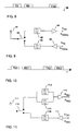
- Figure 4 illustrates another RF front end arrangement according to the invention, suited to be used in the communication system of figure 2.
- the signal received by the antenna 41 is brought to a band pass filter 42 and to a band pass filter 44.
- the pass band of the filter 42 is set so that the RX band is located at the pass band of the filter.
- the received signal is thus switched, via the filter 42, to the amplifier 43, from the output whereof there is obtained an amplified, received signal S RX ⁇
- the pass band of the filter 44 is designed so that both the TDD band and the TX band are located at the pass band of the filter 44. While receiving a signal at the TDD band, the signal received by the antenna 41 thus proceeds through the filter 44, and the filtered signal is directed, by a switch 45, further to the amplifier 43. From the amplifier output, there is obtained a signal S TDDrx for further processing.
- the signal S TX or S TDDtx While transmitting a signal at the TX or TDD band, the signal S TX or S TDDtx is directed to an amplifier 46, and the amplified signal obtained from the output thereof is directed, by the switch 45, to the band pass filter 44. As was already maintained, the filter 44 passes both the TDD and the TX band. The filtered transmission signal is further switched to the antenna 41.
- Figure 5 illustrates the frequency bands used by a communication system on the frequency axis f.
- the transmitter frequency band TX and the receiver frequency band RX for the first communication procedure, there are reserved separate frequency bands, the transmitter frequency band TX and the receiver frequency band RX, and for the second communication procedure, there is reserved the frequency band TDD, which is used in both reception and transmission.
- the employed frequency bands are located on the frequency axis so that the TDD band and the RX band are located near to each other, and the TX band is located further away of said bands.
- the communication system illustrated in figure 5 can be for instance a UMTS system. While employing the communication arrangement illustrated in figure 5, similar filtering operations are assumed of the transceiver as was explained above, in the description of figure 2.
- Figure 6 illustrates an RF front end system according to the invention, suited to be used in a communication arrangement of figure 5.
- the signal received by the antenna 61 is there directed, by a switch 62, to a band pass filter 63.
- the pass band of the filter 63 is designed so that both the TDD band and the RX band are located at the pass band of the filter 63.
- the filtered signal is amplified in an amplifier 64, from the output whereof there are obtained the received, amplified signals S RX and S TDDrx .
- the signal S TX or S TDDtx is amplified in an amplifier 67, whereafter the signal is directed to band pass filters 65 and 66.
- the pass band of the filter 65 is designed so that the filter passes the TDD band, and consequently while transmitting at the TDD band, the transmitter signal filtered by the filter 65 is directed, by the switch 62, to the antenna 61.
- the pass band of the filter 66 it is designed so that the filter passes the TX band; consequently, while transmitting at the TX band, the transmitter signal filtered by the filter 66 is directed, by the switch 62, to the antenna 61.
- Figure 7 illustrates another RF front end arrangement according to the invention, suited to be used in a communication system of figure 5.
- the signal received by the antenna 71 is switched to a band pass filter 72.
- the pass band of the filter 72 is designed so that both the TD band and the RX band are located at the pass band of the filter 72.
- the filtered, received signal is directed, by a switch 73, to an amplifier 74. From the amplifier output, there are obtained the amplified received signals S RX and S TDDrx .
- the RF signal S RX or S TDDtx to be transmitted is fed into the amplifier 76, the output whereof is coupled to a band pass filter 75.
- the pass band of the filter 75 is designed so that the TX band is located at the pass band of the filter 75, and thus while transmitting at the TX band, the transmitter signal is directed, via the filter 75, to the antenna 71. While transmitting at the TDD band, the transmitter signal is directed, via the switch 73, to the filter 72.
- the TDD band is located at the pass band of the filter 72, and consequently the transmitter signal is switched to the antenna 71 via the filter 72.
- the solution according to figure 7 has the same advantages and drawbacks as the solution according to figure 4.
- Figure 8 illustrates the use of frequency bands in a third communication arrangement. It comprises the receiver band RX and the transmitter band TX, connected to the first system. In the second system both transmission and reception take place at the TDD band. In the arrangement according to figure 8, the distance between the RX and TX bands is shorter than the distance of the TDD band from the RX and TX bands.
- the first system can be for instance a GSM system
- the second system can be for instance a DECT, PCS or AMPS system.
- Figure 9 illustrates an RF front end system according to the invention, suited to be used in a communication arrangement of figure 8.
- the signal received by the antenna 91 is there directed by a switch 92 to a filter 93.
- the pass band of the filter 93 is designed so that both the RX band and the TDD band are located at the pass band of the filter 93.
- the filter 93 should have attenuation both at the TX band and in between the RX and TDD bands.
- One alternative is to realise the reception filtering with two separate, parallelly connected band pass filters, so that the TDD band is located at the pass band of the first filter and the RX band is located at the pass band of the second filter.
- the filtered signal is further directed to an amplifier 94, from the output whereof there is obtained a received, amplified RX band signal S RX and TDD band signal S TDDrx ⁇
- the TX band signal S TX or the TDD band signal S TDDtx is fed into an RF power amplifier 96 and the amplified signal is further directed to a band pass filter 95.
- the pass band of the filter 95 is designed so that both the TX band and the TDD band are located at the pass band of the filter 95. If the transmitter spectrum is clean, the attenuation requirements of the stop band of the filter 95 are easily met.
- the filtered signal is further directed, by the switch 92, to the antenna 91.
- Figure 10 illustrates the use of frequency bands in a fourth communication arrangement. It comprises a receiver band RX1 and transmitter band TX1 connected to the first system. In the second system reception takes place at the receiver band RX2, and transmission takes place at the transmitter band TX2. In an arrangement according to figure 10, the distance between the RX and TX bands of the same system is shorter than the distance between the RX and TX bands of two different systems.
- the first and second system can be for example a GSM and a PCN system.
- Figure 11 illustrates an RF front end arrangement according to the invention, suited to be used in connection with the communication arrangement of figure 10.
- the signal received by the antenna 111 is there directed by a switch 112 to filters 113 and 114.
- the pass band of the filter 113 is designed so that the first receiver band RX1 is at the pass band of the filter 113.
- the pass band of the filter 114 is designed so that the second receiver band RX2 is at the pass band of the filter 114.
- the received signal passes either the filter 113 or the filter 114, depending on whether the reception takes place at the band RX 1 or the band RX2.
- the filtered signal is further directed to an amplifier 115, from the output whereof there are obtained the RX1 band signal S RX1 and the RX2 band signal S RX2 .
- an amplifier 115 By means of two parallelly connected filters, a high stop band attenuation is achieved in between the RX1 and RX2 bands.
- the parallel coupling of the filters requires a matching of the impedances, as was explained in connection with the description of figure 3.
- the TX1 band signal S TX1 or the TX2 band signal S TX2 is fed into an RF power amplifier 117.
- the amplified signal is directed to a band pass filter 116, the pass band whereof is designed so that both the band TX1 and the band TX2 are located at the filter pass band.
- the filtered transmitter signal is further directed, by the switch 112, to the antenna 111.
- the transmitter has a clean spectrum, in which case a high attenuation of the stop band is not needed.
- a drawback with solutions where the transmitter signal of the TX or TDD band proceeds unattenuated to the receiver is that another telephone located nearby can cause saturation of the receiver.
- the raising of the saturation point usually means an increase in the power consumption of the receiver, but in TDD reception the saturation point can be effectively raised without any significant increase in the power consumption, because the receiver is on only momentarily in between the reception time slots.
- switches located in the RF signal path are, depending on the transceiver operation and employed frequency range. Said switches are controlled for instance by a processor included in the mobile station. In the memory of the mobile station, there is stored a control programme whereby the processor creates control signals for the switches.
- the control programme takes care that the switch is controlled so that during the time slot reserved for transmission, the transmitter signal is directed from the transmitter to the antenna, and during the time slot reserved for reception, the receiver signal is directed from the antenna to the receiver.
- control programme When the control programme detects in the mobile communications network a command for switching frequency range, it creates a control signal for the switch and controls the switch as was explained in the description of the preferred embodiment above.
- the same control signal path can be used for the selection of both reception, transmission and frequency band selection.
- the processor creates a control command for the switch on the basis of a command given from the user interface, for instance from the keyboard.
- Arrangements according to the invention can be used in a mobile station operating with two different mobile communications systems at two different frequency bands, and in a mobile station operating at two different frequency bands.
- the solutions of the invention for creating the frequencies required in the reception can also be used in a paging device of a paging system operating at two different frequency bands, wherefore the invention is not exclusively limited to mobile telephones.
Landscapes
- Engineering & Computer Science (AREA)
- Computer Networks & Wireless Communication (AREA)
- Signal Processing (AREA)
- Transceivers (AREA)
Applications Claiming Priority (2)
| Application Number | Priority Date | Filing Date | Title |
|---|---|---|---|
| FI962895A FI117841B (fi) | 1996-07-18 | 1996-07-18 | Järjestely radiotaajuisen signaalin lähettämiseksi ja vastaanottamiseksi kahdella taajuusalueella |
| FI962895 | 1996-07-18 |
Publications (3)
| Publication Number | Publication Date |
|---|---|
| EP0820154A2 true EP0820154A2 (fr) | 1998-01-21 |
| EP0820154A3 EP0820154A3 (fr) | 2000-05-10 |
| EP0820154B1 EP0820154B1 (fr) | 2005-10-12 |
Family
ID=8546409
Family Applications (1)
| Application Number | Title | Priority Date | Filing Date |
|---|---|---|---|
| EP97660082A Expired - Lifetime EP0820154B1 (fr) | 1996-07-18 | 1997-07-14 | Radio émetteur-récepteur à deux bandes |
Country Status (4)
| Country | Link |
|---|---|
| US (1) | US6014551A (fr) |
| EP (1) | EP0820154B1 (fr) |
| DE (1) | DE69734338T2 (fr) |
| FI (1) | FI117841B (fr) |
Cited By (6)
| Publication number | Priority date | Publication date | Assignee | Title |
|---|---|---|---|---|
| EP1148655A1 (fr) * | 2000-04-19 | 2001-10-24 | Infineon Technologies AG | Emetteur-récepteur |
| EP1175018A1 (fr) * | 2000-07-19 | 2002-01-23 | Nokia Mobile Phones Ltd. | Circuit d'entrée multimode et appareil de communication sans fil |
| FR2814316A1 (fr) * | 2000-09-20 | 2002-03-22 | Sagem | Emetteur recepteur umts bimode |
| EP1111865A3 (fr) * | 1999-12-20 | 2004-01-07 | Nortel Networks Limited | Dispositif de couplage de récepteur directionel pour liaison d'abonné numérique, à fréquence sélectable et gain réglable |
| US7123897B2 (en) | 1999-09-23 | 2006-10-17 | Nortel Networks Limited | Directional receiver coupling arrangement with frequency selectivity and gain control for DSL |
| CN100341252C (zh) * | 2002-04-08 | 2007-10-03 | 诺基亚有限公司 | 射频前端和提高射频前端的使用灵活性的方法 |
Families Citing this family (73)
| Publication number | Priority date | Publication date | Assignee | Title |
|---|---|---|---|---|
| JP3250796B2 (ja) * | 1998-05-26 | 2002-01-28 | 松下電器産業株式会社 | 受信機 |
| US8050345B1 (en) * | 1999-08-09 | 2011-11-01 | Kamilo Feher | QAM and GMSK systems |
| US7548787B2 (en) | 2005-08-03 | 2009-06-16 | Kamilo Feher | Medical diagnostic and communication system |
| US7593481B2 (en) * | 1998-08-31 | 2009-09-22 | Kamilo Feher | CDMA, W-CDMA, 3rd generation interoperable modem format selectable (MFS) systems with GMSK modulated systems |
| US7415066B2 (en) * | 1998-08-10 | 2008-08-19 | Kamilo Feher | Mis-matched modulation-demodulation format selectable filters |
| US7079584B2 (en) * | 1998-08-10 | 2006-07-18 | Kamilo Feher | OFDM, CDMA, spread spectrum, TDMA, cross-correlated and filtered modulation |
| US6470055B1 (en) * | 1998-08-10 | 2002-10-22 | Kamilo Feher | Spectrally efficient FQPSK, FGMSK, and FQAM for enhanced performance CDMA, TDMA, GSM, OFDN, and other systems |
| US6694128B1 (en) | 1998-08-18 | 2004-02-17 | Parkervision, Inc. | Frequency synthesizer using universal frequency translation technology |
| US7515896B1 (en) | 1998-10-21 | 2009-04-07 | Parkervision, Inc. | Method and system for down-converting an electromagnetic signal, and transforms for same, and aperture relationships |
| US6061551A (en) | 1998-10-21 | 2000-05-09 | Parkervision, Inc. | Method and system for down-converting electromagnetic signals |
| US7039372B1 (en) * | 1998-10-21 | 2006-05-02 | Parkervision, Inc. | Method and system for frequency up-conversion with modulation embodiments |
| US6542722B1 (en) * | 1998-10-21 | 2003-04-01 | Parkervision, Inc. | Method and system for frequency up-conversion with variety of transmitter configurations |
| US6813485B2 (en) | 1998-10-21 | 2004-11-02 | Parkervision, Inc. | Method and system for down-converting and up-converting an electromagnetic signal, and transforms for same |
| US6061555A (en) | 1998-10-21 | 2000-05-09 | Parkervision, Inc. | Method and system for ensuring reception of a communications signal |
| US7236754B2 (en) | 1999-08-23 | 2007-06-26 | Parkervision, Inc. | Method and system for frequency up-conversion |
| US7027786B1 (en) | 1998-10-21 | 2006-04-11 | Parkervision, Inc. | Carrier and clock recovery using universal frequency translation |
| US6370371B1 (en) | 1998-10-21 | 2002-04-09 | Parkervision, Inc. | Applications of universal frequency translation |
| US6560301B1 (en) | 1998-10-21 | 2003-05-06 | Parkervision, Inc. | Integrated frequency translation and selectivity with a variety of filter embodiments |
| US7209725B1 (en) | 1999-01-22 | 2007-04-24 | Parkervision, Inc | Analog zero if FM decoder and embodiments thereof, such as the family radio service |
| US6704558B1 (en) | 1999-01-22 | 2004-03-09 | Parkervision, Inc. | Image-reject down-converter and embodiments thereof, such as the family radio service |
| US6704549B1 (en) * | 1999-03-03 | 2004-03-09 | Parkvision, Inc. | Multi-mode, multi-band communication system |
| US7006805B1 (en) | 1999-01-22 | 2006-02-28 | Parker Vision, Inc. | Aliasing communication system with multi-mode and multi-band functionality and embodiments thereof, such as the family radio service |
| US6853690B1 (en) * | 1999-04-16 | 2005-02-08 | Parkervision, Inc. | Method, system and apparatus for balanced frequency up-conversion of a baseband signal and 4-phase receiver and transceiver embodiments |
| US6879817B1 (en) | 1999-04-16 | 2005-04-12 | Parkervision, Inc. | DC offset, re-radiation, and I/Q solutions using universal frequency translation technology |
| US6873836B1 (en) * | 1999-03-03 | 2005-03-29 | Parkervision, Inc. | Universal platform module and methods and apparatuses relating thereto enabled by universal frequency translation technology |
| US7110435B1 (en) | 1999-03-15 | 2006-09-19 | Parkervision, Inc. | Spread spectrum applications of universal frequency translation |
| US7693230B2 (en) * | 1999-04-16 | 2010-04-06 | Parkervision, Inc. | Apparatus and method of differential IQ frequency up-conversion |
| US7110444B1 (en) * | 1999-08-04 | 2006-09-19 | Parkervision, Inc. | Wireless local area network (WLAN) using universal frequency translation technology including multi-phase embodiments and circuit implementations |
| US7065162B1 (en) | 1999-04-16 | 2006-06-20 | Parkervision, Inc. | Method and system for down-converting an electromagnetic signal, and transforms for same |
| US6584090B1 (en) * | 1999-04-23 | 2003-06-24 | Skyworks Solutions, Inc. | System and process for shared functional block CDMA and GSM communication transceivers |
| US6560297B1 (en) * | 1999-06-03 | 2003-05-06 | Analog Devices, Inc. | Image rejection downconverter for a translation loop modulator |
| US7054296B1 (en) * | 1999-08-04 | 2006-05-30 | Parkervision, Inc. | Wireless local area network (WLAN) technology and applications including techniques of universal frequency translation |
| US8295406B1 (en) | 1999-08-04 | 2012-10-23 | Parkervision, Inc. | Universal platform module for a plurality of communication protocols |
| US9307407B1 (en) | 1999-08-09 | 2016-04-05 | Kamilo Feher | DNA and fingerprint authentication of mobile devices |
| US9813270B2 (en) | 1999-08-09 | 2017-11-07 | Kamilo Feher | Heart rate sensor and medical diagnostics wireless devices |
| US7260369B2 (en) | 2005-08-03 | 2007-08-21 | Kamilo Feher | Location finder, tracker, communication and remote control system |
| US9373251B2 (en) | 1999-08-09 | 2016-06-21 | Kamilo Feher | Base station devices and automobile wireless communication systems |
| US7082171B1 (en) | 1999-11-24 | 2006-07-25 | Parkervision, Inc. | Phase shifting applications of universal frequency translation |
| US6963734B2 (en) | 1999-12-22 | 2005-11-08 | Parkervision, Inc. | Differential frequency down-conversion using techniques of universal frequency translation technology |
| US7292835B2 (en) * | 2000-01-28 | 2007-11-06 | Parkervision, Inc. | Wireless and wired cable modem applications of universal frequency translation technology |
| US7010286B2 (en) | 2000-04-14 | 2006-03-07 | Parkervision, Inc. | Apparatus, system, and method for down-converting and up-converting electromagnetic signals |
| US7554508B2 (en) | 2000-06-09 | 2009-06-30 | Parker Vision, Inc. | Phased array antenna applications on universal frequency translation |
| US7010559B2 (en) * | 2000-11-14 | 2006-03-07 | Parkervision, Inc. | Method and apparatus for a parallel correlator and applications thereof |
| US7454453B2 (en) * | 2000-11-14 | 2008-11-18 | Parkervision, Inc. | Methods, systems, and computer program products for parallel correlation and applications thereof |
| FI20002881A7 (fi) * | 2000-12-29 | 2002-06-30 | Nokia Corp | Järjestely ja menetelmä radiolähettimen häviöiden vähentämiseksi |
| JP3873671B2 (ja) * | 2001-06-12 | 2007-01-24 | ソニー株式会社 | 通信装置 |
| US7085335B2 (en) | 2001-11-09 | 2006-08-01 | Parkervision, Inc. | Method and apparatus for reducing DC offsets in a communication system |
| US7072427B2 (en) | 2001-11-09 | 2006-07-04 | Parkervision, Inc. | Method and apparatus for reducing DC offsets in a communication system |
| JP4166466B2 (ja) * | 2001-12-19 | 2008-10-15 | ソニー株式会社 | 無線通信システム及び無線通信方法、無線通信装置及びその制御方法、並びにコンピュータ・プログラム |
| GB0204108D0 (en) * | 2002-02-21 | 2002-04-10 | Analog Devices Inc | 3G radio |
| WO2003073659A2 (fr) * | 2002-02-21 | 2003-09-04 | Analog Devices, Inc. | Radio 3g |
| US6975848B2 (en) | 2002-06-04 | 2005-12-13 | Parkervision, Inc. | Method and apparatus for DC offset removal in a radio frequency communication channel |
| US7321640B2 (en) | 2002-06-07 | 2008-01-22 | Parkervision, Inc. | Active polyphase inverter filter for quadrature signal generation |
| US7460584B2 (en) | 2002-07-18 | 2008-12-02 | Parkervision, Inc. | Networking methods and systems |
| US7379883B2 (en) * | 2002-07-18 | 2008-05-27 | Parkervision, Inc. | Networking methods and systems |
| WO2004036778A1 (fr) * | 2002-10-14 | 2004-04-29 | Koninklijke Philips Electronics N.V. | Commutateur d'antenne d'emission et de reception |
| DE10316719B4 (de) * | 2003-04-11 | 2018-08-02 | Snaptrack, Inc. | Frontendschaltung für drahtlose Übertragungssysteme |
| US7366485B2 (en) * | 2004-03-04 | 2008-04-29 | Matsushita Electric Industrial Co., Ltd. | Multimode wireless transmitter and a portable wireless device using the same |
| US20050245201A1 (en) * | 2004-04-30 | 2005-11-03 | Nokia Corporation | Front-end topology for multiband multimode communication engines |
| US7187945B2 (en) * | 2004-04-30 | 2007-03-06 | Nokia Corporation | Versatile antenna switch architecture |
| US7127216B2 (en) * | 2004-07-06 | 2006-10-24 | Avago Technologies Wireless Ip (Singapore) Pte. Ltd. | Integrated circuit and method for receiving and transmitting signals of different frequency bands |
| US7359449B2 (en) * | 2004-10-05 | 2008-04-15 | Kamilo Feher | Data communication for wired and wireless communication |
| US7421004B2 (en) * | 2004-10-05 | 2008-09-02 | Kamilo Feher | Broadband, ultra wideband and ultra narrowband reconfigurable interoperable systems |
| US20060128425A1 (en) * | 2004-12-13 | 2006-06-15 | Rooyen Pieter V | Method and system for mobile architecture supporting cellular or wireless networks and broadcast utilizing a multichip cellular and broadcast silicon solution |
| US10009956B1 (en) | 2017-09-02 | 2018-06-26 | Kamilo Feher | OFDM, 3G and 4G cellular multimode systems and wireless mobile networks |
| US7280810B2 (en) * | 2005-08-03 | 2007-10-09 | Kamilo Feher | Multimode communication system |
| US7680510B2 (en) * | 2005-11-10 | 2010-03-16 | Alcatel-Lucent Usa Inc. | Diversity-switched front end base station transceiver system |
| CN1992538A (zh) * | 2005-12-30 | 2007-07-04 | 鸿富锦精密工业(深圳)有限公司 | 移动通信装置 |
| US7672645B2 (en) * | 2006-06-15 | 2010-03-02 | Bitwave Semiconductor, Inc. | Programmable transmitter architecture for non-constant and constant envelope modulation |
| KR100819881B1 (ko) * | 2006-08-16 | 2008-04-08 | 삼성전자주식회사 | 듀얼 밴드 디지털 멀티미디어 방송 수신기 |
| JP2009021895A (ja) * | 2007-07-13 | 2009-01-29 | Panasonic Corp | アンテナ共用器とそれを用いた通信機器 |
| FR2939988B1 (fr) * | 2008-12-16 | 2011-07-29 | Thales Sa | Recepteur numerique large bande comprenant un mecanisme de detection des sauts de phase |
| DE102019210496A1 (de) | 2018-07-18 | 2020-01-23 | Skyworks Solutions, Inc. | Hybrides akustisches lc filter mit unterdrückung von harmonischen |
Family Cites Families (11)
| Publication number | Priority date | Publication date | Assignee | Title |
|---|---|---|---|---|
| US5091919A (en) * | 1989-02-08 | 1992-02-25 | Nokia-Mobira Oy | Transmitter arrangement for digitally modulated signals |
| US5123031A (en) * | 1989-02-08 | 1992-06-16 | Nokia-Mobira Oy | Control voltage generator in a transmitter arrangement for digitally modulated signals |
| WO1992000634A1 (fr) * | 1990-06-22 | 1992-01-09 | Motorola, Inc. | Radio avec amplificateur de puissance et modes d'exploitation duplex/semi-duplex |
| JPH04269021A (ja) * | 1991-02-25 | 1992-09-25 | Nec Corp | 双方向ページングシステムおよび該システムに用いられる携帯無線機 |
| JP2840496B2 (ja) * | 1992-02-26 | 1998-12-24 | 三洋電機株式会社 | デュアルバンド無線通信装置 |
| GB2278253B (en) * | 1993-05-05 | 1996-08-28 | Marconi Gec Ltd | An integrated transceiver circuit packaged component |
| US5590412A (en) * | 1993-11-19 | 1996-12-31 | Sanyo Electric Co., Ltd. | Communication apparatus using common amplifier for transmission and reception |
| FI941862A7 (fi) * | 1994-04-21 | 1995-10-22 | Nokia Mobile Phones Ltd | Menetelmä ja radiotaajuusjärjestelmä kahden eri taajuusalueella toimivan radioviestinjärjestelmän vastaanottimen ja lähettimen taajuuksien muodostamiseksi ja kahdella eri taajuusalueella toimiva vastaanotin ja lähetin sekä edellisten käyttö matkapuhelimessa |
| JP2586333B2 (ja) * | 1994-05-13 | 1997-02-26 | 日本電気株式会社 | 無線通信装置 |
| US5758266A (en) * | 1994-09-30 | 1998-05-26 | Qualcomm Incorporated | Multiple frequency communication device |
| EP1146638B1 (fr) * | 1995-05-16 | 2003-10-29 | Matsushita Electric Industrial Co., Ltd. | Unité sans fil pour système à accès multiple et à division dans le temps |
-
1996
- 1996-07-18 FI FI962895A patent/FI117841B/fi not_active IP Right Cessation
-
1997
- 1997-07-14 EP EP97660082A patent/EP0820154B1/fr not_active Expired - Lifetime
- 1997-07-14 DE DE69734338T patent/DE69734338T2/de not_active Expired - Lifetime
- 1997-07-16 US US08/893,952 patent/US6014551A/en not_active Expired - Lifetime
Cited By (8)
| Publication number | Priority date | Publication date | Assignee | Title |
|---|---|---|---|---|
| US7123897B2 (en) | 1999-09-23 | 2006-10-17 | Nortel Networks Limited | Directional receiver coupling arrangement with frequency selectivity and gain control for DSL |
| EP1111865A3 (fr) * | 1999-12-20 | 2004-01-07 | Nortel Networks Limited | Dispositif de couplage de récepteur directionel pour liaison d'abonné numérique, à fréquence sélectable et gain réglable |
| EP1148655A1 (fr) * | 2000-04-19 | 2001-10-24 | Infineon Technologies AG | Emetteur-récepteur |
| WO2001082493A1 (fr) * | 2000-04-19 | 2001-11-01 | Infineon Technologies Ag | Unite d'emission-reception |
| EP1175018A1 (fr) * | 2000-07-19 | 2002-01-23 | Nokia Mobile Phones Ltd. | Circuit d'entrée multimode et appareil de communication sans fil |
| FR2814316A1 (fr) * | 2000-09-20 | 2002-03-22 | Sagem | Emetteur recepteur umts bimode |
| EP1191702A1 (fr) * | 2000-09-20 | 2002-03-27 | Sagem SA | Emetteur récepteur UMTS bimode |
| CN100341252C (zh) * | 2002-04-08 | 2007-10-03 | 诺基亚有限公司 | 射频前端和提高射频前端的使用灵活性的方法 |
Also Published As
| Publication number | Publication date |
|---|---|
| US6014551A (en) | 2000-01-11 |
| FI962895A0 (fi) | 1996-07-18 |
| DE69734338T2 (de) | 2006-06-22 |
| FI962895L (fi) | 1998-01-19 |
| DE69734338D1 (de) | 2005-11-17 |
| EP0820154B1 (fr) | 2005-10-12 |
| FI117841B (fi) | 2007-03-15 |
| EP0820154A3 (fr) | 2000-05-10 |
Similar Documents
| Publication | Publication Date | Title |
|---|---|---|
| EP0820154B1 (fr) | Radio émetteur-récepteur à deux bandes | |
| RU2214050C2 (ru) | Устройство связи для приема сигналов связи во множестве радиочастотных полос (варианты) и способ для приема сигналов из множества полос | |
| EP0678974B1 (fr) | Emetteur et/ou récepteur | |
| US5974305A (en) | Dual band architectures for mobile stations | |
| US7725082B2 (en) | Radio communication apparatus, radio communication method, antenna apparatus and first duplexer | |
| US6256511B1 (en) | Dual-mode radio architecture | |
| US5881369A (en) | Dual mode transceiver | |
| EP1059734B1 (fr) | Radioémetteur-recepteur pour opération à deux gammes de fréquences | |
| US6584090B1 (en) | System and process for shared functional block CDMA and GSM communication transceivers | |
| US6405025B1 (en) | Method for selecting the frequency range in radio communication devices operating in several frequency ranges and a radio communication device | |
| EP1105973B1 (fr) | Radiotéléphone à double bande avec antennes affectées à l'émission et à la réception | |
| EP0486181B1 (fr) | Téléphone radio-mobile | |
| EP1111821B1 (fr) | Dispositif de combinaison dans un système sans fil et son procédé | |
| US5659886A (en) | Digital mobile transceiver with phase adjusting strip lines connecting to a common antenna | |
| KR100406869B1 (ko) | 주파수 다중 트랜시버 및 크로스토크를 제거하기 위한 방법 | |
| GB2344236A (en) | Multiple band mixer with common local oscillator | |
| US5815805A (en) | Apparatus and method for attenuating an undesired signal in a radio transceiver | |
| EP0923198A2 (fr) | Procedé de sélection de bande de fréquence pour dispositif de communication multibande , et dispositif de communication | |
| CN112994729B (zh) | 一种移动终端射频模块及移动终端 | |
| WO1998011674A1 (fr) | Procede et appareil permettant de supprimer les harmoniques superieurs d'emetteur ainsi que les signaux de blocage de recepteur | |
| KR20030060612A (ko) | 멀티 채널의 중간주파수 처리기 및 그를 이용한 멀티채널의 중계 장치 | |
| KR100469411B1 (ko) | 이동통신 단말기의 안테나 매칭회로 | |
| MXPA98001327A (es) | Metodo y aparato para recibir señales decomunicacion | |
| WO2003103156A2 (fr) | Circuit radioelectrique | |
| MXPA99001788A (en) | A system and method for achieving extended radio coverage and additional capacity using extended frequency bands |
Legal Events
| Date | Code | Title | Description |
|---|---|---|---|
| PUAI | Public reference made under article 153(3) epc to a published international application that has entered the european phase |
Free format text: ORIGINAL CODE: 0009012 |
|
| AK | Designated contracting states |
Kind code of ref document: A2 Designated state(s): DE FR GB IT SE |
|
| PUAL | Search report despatched |
Free format text: ORIGINAL CODE: 0009013 |
|
| AK | Designated contracting states |
Kind code of ref document: A3 Designated state(s): AT BE CH DE DK ES FI FR GB GR IE IT LI LU MC NL PT SE |
|
| 17P | Request for examination filed |
Effective date: 20001110 |
|
| AKX | Designation fees paid |
Free format text: DE FR GB IT SE |
|
| RAP1 | Party data changed (applicant data changed or rights of an application transferred) |
Owner name: NOKIA CORPORATION |
|
| 17Q | First examination report despatched |
Effective date: 20040211 |
|
| GRAP | Despatch of communication of intention to grant a patent |
Free format text: ORIGINAL CODE: EPIDOSNIGR1 |
|
| GRAS | Grant fee paid |
Free format text: ORIGINAL CODE: EPIDOSNIGR3 |
|
| GRAA | (expected) grant |
Free format text: ORIGINAL CODE: 0009210 |
|
| AK | Designated contracting states |
Kind code of ref document: B1 Designated state(s): DE FR GB IT SE |
|
| REG | Reference to a national code |
Ref country code: GB Ref legal event code: FG4D |
|
| REG | Reference to a national code |
Ref country code: SE Ref legal event code: TRGR |
|
| REF | Corresponds to: |
Ref document number: 69734338 Country of ref document: DE Date of ref document: 20051117 Kind code of ref document: P |
|
| ET | Fr: translation filed | ||
| PLBE | No opposition filed within time limit |
Free format text: ORIGINAL CODE: 0009261 |
|
| STAA | Information on the status of an ep patent application or granted ep patent |
Free format text: STATUS: NO OPPOSITION FILED WITHIN TIME LIMIT |
|
| 26N | No opposition filed |
Effective date: 20060713 |
|
| REG | Reference to a national code |
Ref country code: GB Ref legal event code: 732E Free format text: REGISTERED BETWEEN 20110106 AND 20110112 |
|
| REG | Reference to a national code |
Ref country code: DE Ref legal event code: R081 Ref document number: 69734338 Country of ref document: DE Owner name: RENESAS ELECTRONICS CORPORATION, KAWASAKI, JP Free format text: FORMER OWNER: NOKIA CORP., 02610 ESPOO, FI Effective date: 20110217 Ref country code: DE Ref legal event code: R081 Ref document number: 69734338 Country of ref document: DE Owner name: RENESAS ELECTRONICS CORPORATION, KAWASAKI, JP Free format text: FORMER OWNER: NOKIA CORP., ESPOO, FI Effective date: 20110217 |
|
| REG | Reference to a national code |
Ref country code: FR Ref legal event code: TP Owner name: RENESAS ELECTRONICS CORPORATION, JP Effective date: 20130626 |
|
| REG | Reference to a national code |
Ref country code: FR Ref legal event code: PLFP Year of fee payment: 19 |
|
| PGFP | Annual fee paid to national office [announced via postgrant information from national office to epo] |
Ref country code: GB Payment date: 20150708 Year of fee payment: 19 Ref country code: DE Payment date: 20150707 Year of fee payment: 19 |
|
| PGFP | Annual fee paid to national office [announced via postgrant information from national office to epo] |
Ref country code: SE Payment date: 20150713 Year of fee payment: 19 Ref country code: FR Payment date: 20150629 Year of fee payment: 19 |
|
| PGFP | Annual fee paid to national office [announced via postgrant information from national office to epo] |
Ref country code: IT Payment date: 20150727 Year of fee payment: 19 |
|
| REG | Reference to a national code |
Ref country code: DE Ref legal event code: R119 Ref document number: 69734338 Country of ref document: DE |
|
| REG | Reference to a national code |
Ref country code: SE Ref legal event code: EUG |
|
| GBPC | Gb: european patent ceased through non-payment of renewal fee |
Effective date: 20160714 |
|
| PG25 | Lapsed in a contracting state [announced via postgrant information from national office to epo] |
Ref country code: DE Free format text: LAPSE BECAUSE OF NON-PAYMENT OF DUE FEES Effective date: 20170201 Ref country code: FR Free format text: LAPSE BECAUSE OF NON-PAYMENT OF DUE FEES Effective date: 20160801 Ref country code: SE Free format text: LAPSE BECAUSE OF NON-PAYMENT OF DUE FEES Effective date: 20160715 |
|
| REG | Reference to a national code |
Ref country code: FR Ref legal event code: ST Effective date: 20170331 |
|
| PG25 | Lapsed in a contracting state [announced via postgrant information from national office to epo] |
Ref country code: GB Free format text: LAPSE BECAUSE OF NON-PAYMENT OF DUE FEES Effective date: 20160714 |
|
| PG25 | Lapsed in a contracting state [announced via postgrant information from national office to epo] |
Ref country code: IT Free format text: LAPSE BECAUSE OF NON-PAYMENT OF DUE FEES Effective date: 20160714 |