EP0821387A2 - Tube à rayons cathodiques - Google Patents
Tube à rayons cathodiques Download PDFInfo
- Publication number
- EP0821387A2 EP0821387A2 EP97111891A EP97111891A EP0821387A2 EP 0821387 A2 EP0821387 A2 EP 0821387A2 EP 97111891 A EP97111891 A EP 97111891A EP 97111891 A EP97111891 A EP 97111891A EP 0821387 A2 EP0821387 A2 EP 0821387A2
- Authority
- EP
- European Patent Office
- Prior art keywords
- electrodes
- spacers
- grid
- ray tube
- cathode ray
- Prior art date
- Legal status (The legal status is an assumption and is not a legal conclusion. Google has not performed a legal analysis and makes no representation as to the accuracy of the status listed.)
- Withdrawn
Links
Images


Classifications
-
- H—ELECTRICITY
- H01—ELECTRIC ELEMENTS
- H01J—ELECTRIC DISCHARGE TUBES OR DISCHARGE LAMPS
- H01J29/00—Details of cathode-ray tubes or of electron-beam tubes of the types covered by group H01J31/00
- H01J29/46—Arrangements of electrodes and associated parts for generating or controlling the ray or beam, e.g. electron-optical arrangement
- H01J29/48—Electron guns
- H01J29/485—Construction of the gun or of parts thereof
Definitions
- the invention relates to a cathode ray tube according to the preamble of Claim 1.
- a cathode ray tube in which a ceramic ring as a support body a flat surface and opposite has a truncated cone-shaped depression.
- a first flat grid electrode is on the flat side and a second grid electrode on the opposite Side of the support body attached, the second grid electrode with a Truncated cone section protrudes into the recess.
- the carrier body has a central one Opening in which the two grid electrodes coaxially face aligned jet openings.
- US-A-3032674 describes a grid arrangement for a cathode ray tube, in which metallic disc electrodes by ceramic insulating washers are isolated from each other. The central aperture openings of the Disc electrodes are spanned by fine-meshed electrode grids. Of the layered grid structure is held together by screws.
- the present invention has for its object a cathode ray tube specify, the grid arrangement inexpensive to manufacture with high precision is and leads to improved imaging properties.
- the for the grid arrangement of the cathode ray tube according to the invention Parts used can be manufactured inexpensively and with high precision can be assembled into the connected arrangement.
- the connected Grid arrangement is compact, mechanically stable and easy to handle and can be assembled and checked outside the tube.
- the Spacers ensure high-precision compliance with specified mutual grid electrode spacing without separate adjustment measures.
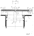
- FIG. 1 outlined grid arrangement shows a preferred application of the invention in a cathode ray tube having a first grating with a Grid electrode G1 and a second grid with two separate, in the beam direction Z successive grid electrodes G21 and G22.
- the grids are used for Focusing and intensity control of that emitted by a cathode K. Electron flow. Structure and attachment of the cathode via a cathode sleeve W and carrier plate P in brackets H are known in various forms and not the subject of the invention.
- the grid electrodes are designed as flat sheets or metal foils with a thickness of typically 0.05 mm to 0.5 mm.
- the central grid electrode G21 is separated from the grid electrode G22 by a spacer S2 and from the grid electrode G1 by a spacer S1 and is electrically insulated from them.
- the spacers are designed as ring disks with a circular inner opening OD.
- the spacers are preferably made of ceramic, in particular Al 2 O 3 ceramic, and are firmly connected to the grid electrodes. Soldering is advantageously used as the connection technique.
- the layer sequence of alternating metallic electrode and ceramic spacer is advantageously closed on both sides by further ceramic members in the form of ring washers SO and S3, which are also soldered to the grid electrodes G1 and G22.
- the spacers S1, S2 and the other ceramic members SO and S3 do not necessarily, but preferably have the same diameter dD circular inner openings.
- the grid electrodes each have one central jet opening OS.
- the diameter of the jet openings are in Usually not uniform for all grid electrodes and with values from 0.1 to 0.7mm small compared to the diameter dD of the spacers typically in the range of 1mm to 5mm.
- the grid electrodes are advantageously made of a material that one has similar thermal expansion coefficients as the material of the Spacers.
- the spacers are made of Al2O3 ceramic and the grid electrodes made of molybdenum, titanium or an alloy with the Designation FeNi42.
- S3 is also quartz with an Al2O3 ceramic lower dielectric constant with a view to reducing the Grid capacity advantageous.
- the thicknesses of the spacers S1, S2 essentially determine that mutual spacing of the grid electrodes.
- the thicknesses of the spacers are typically in the range of 0.05mm to 1.0mm.
- the different Spacers S1, S2 generally have different thicknesses.
- For the mutual distance between the grid electrodes may still be the thickness of Solder layers between the spacer and grid electrodes to be observed and at the Dimensioning to take into account.
- Solder foils typically have a thickness of 5 ⁇ m to 40 ⁇ m going out.
- the Surfaces of grid electrodes and spacers can be provided with coatings suitable for soldering.
- Other techniques in which the materials of the grid electrodes (and Ring links) and the spacers are coordinated so that a firm connection can be made without intermediate material are also advantageous suitable.
- copper-containing molybdenum sheets at high Temperatures copper diffuse to the sheet surface and there a solid Create a connection with the ceramic of the spacers.
- the grid electrodes are preferably previously with the beam openings provided and by means of a centering gauge, e.g. a thorn, they can various grid electrodes with coaxial alignment of the beam openings be adjusted.
- the elements of the stack are heated together soldered and result in a compact, mechanically stable and easy to handle Grid arrangement, which with the other components of the beam generation and Focusing system, in particular the cathode arrangement is connected. Compliance with an important distance of the first grid electrode G1 from the The cathode can be pre-assembled and adjusted separately Cathode assembly with cathode sleeve W, support plate P, brackets H and Spacer ring R can be guaranteed
- a grid arrangement with circular disk-shaped grid electrodes G1, G21, G22 similar to the arrangement known from US-A-3032674 would because of the large opposing areas and the small electrode spacing show relatively high capacitance between the grid electrodes, which at Control one or more of these grids with a high frequency Control signal adversely affects the maximum signal frequency.
- the grid electrodes are advantageously reduced in this way to reduce the grid capacity structured and arranged so that there is as little overlap as possible Results in electrode areas.
- FIG. 2 (A) and (B) outlined advantageous examples of a design from grid electrodes to a connected arrangement with three grid electrodes G1, G21, G22 as in the example from FIG. 1 each have a central part M around the Jet opening OS, which preferably has a substantially circular contour shows and its diameter in the range of the diameter of the inner opening OD of the spacer S is and preferably less than 30% of this deviates.
- the middle part is a control signal carrying section U of the Grid electrode connected to the terminal lug A.
- the diameter of the central part is larger than that of the inner opening OD, so that the middle part along its entire circumference between two neighboring ones Spacers or additional ring links S is sufficient and is held there.
- the diameter of the middle part is smaller than the inner opening OD.
- the middle section is then over section U and possibly one or more extending into the area between the links S. Retaining tabs L held.
- the connecting section U takes up less than one Third circle segment of the area between the links S and can also significantly narrower, in particular for the function of the signal feed be.
- In the surface areas not occupied by the grid electrode further elements N are arranged between the links S and are the same Thickness like that of section U of the grid electrode. These others Elements N fulfill the mechanical function of the fixed connection of the links S while ensuring parallel alignment of connected links S.
- Grid electrodes further elements N and a possibly existing solder layer in the plane perpendicular to the beam axis in electrically insulated areas structured with the goal of low grid capacity.
- suitable structures are a multitude of possibilities conceivable, each of which also mechanical properties and manageability during manufacture Can be considered.
- the grid electrodes are in Cover the direction parallel to the beam axis Z as little as possible and other conductor structures with little or no common coverage show different grid electrodes. The coverage of the electrodes in the The area around the jet openings are for electrical functional reasons unavoidable and cause a minimum capacity of the grid arrangement.
- FIG. 2 (A) and (B) outlined design of the grid electrodes and the additional elements N with a conductive divided into three circular ring segments Layer between two insulating links S enables use largely identical structures in the three grid electrode levels of the Arrangement according to FIG. 1, which is then only in the layer thickness and the width of the jet openings need to be distinguished, the Connection sections of the grid electrodes in the different levels, respectively are rotated by 120 degrees to each other. The result is simple buildable mechanically stable arrangement with very low grid capacity.
- FIG. 3 are from the variety of suitable structures of the conductor layers further examples of similar structuring in three ladder levels are outlined.
- FIG. 3 (A) are the individual grid electrodes in the form of Circular rings and narrow radial feed webs between the connection lug and middle section, whereby a slight overlap is achieved that the circular rings have different radii and the radial ones Supply webs are aligned at an angle.
- FIG. 3 (B) sees narrow lead webs between the grid electrodes Connection lugs and middle parts and additionally two retaining straps for each Middle part in front.
- the different grid electrodes are twisted against each other arranged that neither the feed webs nor the retaining tabs Have overlaps.
- the mechanical stability can be increased by Electrically insulated circular rings interrupted on the supply webs.
- the execution according to FIG. 3 (C) can be from the embodiment of FIG. 2 derived instead of extending over a wide radius range Circular rings of approximately 120 degrees narrower each and the Connection sections U are slimmed to connecting webs.
- G is a grid electrode denotes, which is a connection tab A, a lead section U, a Middle part M with central jet opening OS and one over the middle part protruding holding element U '.
- insulating ceramic segments KS are outlined, which are used for the composition the arrangement can be moved closer to the electrodes G and with their outer and inner circumferences preferably circles around the central beam opening OS describe with inner circle radius ri and outer circle radius ra.
- the moving together of the ceramic segments KS towards the electrode G is complete Arrows indicated at the bottom of the ceramic segments KS.
- the Ceramic segments KS and the grid electrode G have at least approximately that same thickness perpendicular to the plane of the drawing. This thickness is, for example in the range of 150 ⁇ m.
- FIG. 4 also outlines a ring of soldering segments LS, which are arranged regularly around the beam axis. In the radial direction from the From the beam axis, these soldering segments LS are dimensioned and arranged that its edge facing the beam axis is at a greater distance from Beam axis has the inner circle radius of the ceramic segments KS. The the Edge of the soldering segments LS facing away from the beam axis is closer to the beam axis than the outer radius of the ceramic segments KS.
- the number of solder segments within a wreath and thus their angular extent depends on the Number of grid electrodes of the grid arrangement and is at described preferred construction four times the number of Grid electrodes.
- soldering segments LS with a mutual angular offset of 30 degrees and an angular expansion of less than 30 degrees per soldering segment ring intended.
- the thickness of the solder segments perpendicular to the plane of the drawing 4 is generally much smaller than the thickness of the ceramic segments KS and grid electrode E and is typically 25 ⁇ m.
- annular spacers made of insulating Material, preferably ceramic provided. These are in the order of the 1 with S0 S1, S2 and S3.
- the longitudinal axes of the electrode parts E in successive electrode layers preferably at regular angles of 120 degrees offset from each other in the example.
- the solder segment layers can each contain a complete ring of soldering segments.
- the segment positions which are perpendicular to the Layer levels in extension of an electrode position and not directly at one Electrode lie, not occupied, to avoid capacitive influences on undefined Avoid potential floating conductive layers as much as possible.
- the plurality of grid electrodes G1, G21 and G22 are each offset by 120 degrees from one another and overlap with their central parts M.
- the beam openings OS and central parts M are concentric about the beam axis.
- the electrodes in the lead sections U and the holding sections U ' show no overlap with one another and also not indirectly via the conductive soldering segments LS.
- the hatched areas indicate a further embodiment of the grid electrodes, in which the electrodes are partially etched thinner in the hatched areas and are therefore only soldered to the adjacent ceramic spacers in the edge areas of the supply and holding sections.
- FIG. 5 are with T1, T2, T3, « successive angle segments in the Designated clockwise, on which the representation of FIG. 6 is based.
- the FIG. 6 shows the layering of the arrangement according to FIG. 5 in the form of a Scope processing with subdivision into segments according to a Progress along a rotation angle from 0 degrees to 360 degrees.
- the Layer representation is differentiated between a layer LD of one annular insulating spacer B, a solder segment layer LL with ring-shaped soldering segments LS, and an electrode layer LE with Grid electrodes and insulating ceramic segments KS.
- Both the Spacers S and the electrode layers LE are not necessarily of the same thickness rather can be varied by variation in particular the spacing of the grid electrodes the field course in the area of the beam openings to be influenced.
- the layer structure with alternating spacers and Electrode layers with interposed solder segment layers is under reference on FIG 1 and FIG 5 need no further explanation.
- the invention is not restricted to the examples outlined in detail but within the scope of professional skill in a variety of Embodiments can be implemented.
- the number of grid electrodes variable.
- the outer contour of the connected arrangement is not necessary circular and spacers and grid electrodes can be different Have outer contours.
Landscapes
- X-Ray Techniques (AREA)
- Electrodes For Cathode-Ray Tubes (AREA)
- Measurement Of Radiation (AREA)
Applications Claiming Priority (2)
| Application Number | Priority Date | Filing Date | Title |
|---|---|---|---|
| DE19630200 | 1996-07-26 | ||
| DE19630200A DE19630200A1 (de) | 1996-07-26 | 1996-07-26 | Kathodenstrahlröhre |
Publications (2)
| Publication Number | Publication Date |
|---|---|
| EP0821387A2 true EP0821387A2 (fr) | 1998-01-28 |
| EP0821387A3 EP0821387A3 (fr) | 1999-05-06 |
Family
ID=7800927
Family Applications (1)
| Application Number | Title | Priority Date | Filing Date |
|---|---|---|---|
| EP97111891A Withdrawn EP0821387A3 (fr) | 1996-07-26 | 1997-07-12 | Tube à rayons cathodiques |
Country Status (3)
| Country | Link |
|---|---|
| US (1) | US5942847A (fr) |
| EP (1) | EP0821387A3 (fr) |
| DE (1) | DE19630200A1 (fr) |
Families Citing this family (6)
| Publication number | Priority date | Publication date | Assignee | Title |
|---|---|---|---|---|
| US6133685A (en) * | 1996-07-05 | 2000-10-17 | Matsushita Electronics Corporation | Cathode-ray tube |
| US6320333B1 (en) | 1997-02-07 | 2001-11-20 | Matsushita Electric Industrial Co., Ltd. | Color picture tube |
| JP3528526B2 (ja) | 1997-08-04 | 2004-05-17 | 松下電器産業株式会社 | カラー受像管装置 |
| JPH1167121A (ja) | 1997-08-27 | 1999-03-09 | Matsushita Electron Corp | 陰極線管 |
| DE10118652A1 (de) * | 2001-04-14 | 2002-10-17 | Thales Electron Devices Gmbh | Kathodenstrahlröhre |
| US7135821B2 (en) * | 2003-10-01 | 2006-11-14 | Altera Corporation | High-definition cathode ray tube and electron gun |
Family Cites Families (6)
| Publication number | Priority date | Publication date | Assignee | Title |
|---|---|---|---|---|
| US2227087A (en) * | 1937-06-30 | 1940-12-31 | Siemens Ag | Cathode ray tube |
| BE572426A (fr) * | 1957-10-30 | |||
| NL266799A (fr) * | 1961-07-07 | |||
| GB2046511B (en) * | 1979-04-09 | 1983-04-20 | Tektronix Inc | Electron gun having a low capacitance cathode and grid assembly |
| DE19534123A1 (de) * | 1995-09-14 | 1997-03-20 | Licentia Gmbh | Kathodenstrahlröhre |
| DE19534124A1 (de) * | 1995-09-14 | 1997-03-20 | Licentia Gmbh | Kathodenstrahlröhre |
-
1996
- 1996-07-26 DE DE19630200A patent/DE19630200A1/de not_active Withdrawn
-
1997
- 1997-07-12 EP EP97111891A patent/EP0821387A3/fr not_active Withdrawn
- 1997-07-24 US US08/899,727 patent/US5942847A/en not_active Expired - Fee Related
Also Published As
| Publication number | Publication date |
|---|---|
| US5942847A (en) | 1999-08-24 |
| DE19630200A1 (de) | 1998-01-29 |
| EP0821387A3 (fr) | 1999-05-06 |
Similar Documents
| Publication | Publication Date | Title |
|---|---|---|
| EP1200970B1 (fr) | Varistor multicouche de faible capacite | |
| DE19834461C2 (de) | Vielschicht-Piezoaktor | |
| DE69020747T2 (de) | Eine die Ablenkung kompensierende Vorrichtung für konvergierende Linsen. | |
| EP0821387A2 (fr) | Tube à rayons cathodiques | |
| DE3686202T2 (de) | Elektronenkanone. | |
| DE3781666T2 (de) | Elektronenstrahlgeraet und fokussierlinse fuer ein solches geraet. | |
| EP0360906B1 (fr) | Intensificateur d'images de rayons X | |
| DE68926172T2 (de) | Elektronenstrahlröhre | |
| EP0240769B1 (fr) | Plaque de commande pour des dispositifs de reproduction d'images | |
| DE8915750U1 (de) | Kontaktanordnung für eine Vakuumschaltröhre | |
| DE3032486C2 (de) | Elektronenstrahlsystem für Fernsehbildröhren | |
| EP3105562B1 (fr) | Cellule de mesure de pression | |
| DE69302998T2 (de) | Elektronenkanone für eine Kathodenstrahlröhre | |
| DD151533A5 (de) | Vorbeschichtete widerstandsbehaftete linsenstruktur fuer ein elektronenstrahlsystem und verfahren zu dessen herstellung | |
| DE4219806A1 (de) | Filtersteckverbinder | |
| DE2914631A1 (de) | Heizer-katode-einheit geringer masse mit schnellheizeigenschaft | |
| DE3102183C2 (de) | Elektronenstrahlsystem für Fernsehbildröhren | |
| EP0187951B1 (fr) | Contact interrupteur pour un interrupteur sous vide | |
| EP1535364B1 (fr) | Element d'attenuation ou de terminaison a structure coaxiale pour ondes electromagnetiques haute frequence | |
| EP0763846B1 (fr) | Tube à rayons cathodiques | |
| DE2216448C2 (de) | Widerstandsanordnung aus stapelbaren Widerständen | |
| DE3200117C2 (de) | Einbau-Bandpaßfilteranordnung für ein Koaxialkabel | |
| DE2412541C3 (de) | Strahlerzeugersystem für Farbbildröhren | |
| DE3032487C2 (de) | Elektronenstrahlsystem für Fernsehbildröhren | |
| DE2751736C2 (de) | Elektrische Entladungsröhre und Verfahren zu ihrer Herstellung |
Legal Events
| Date | Code | Title | Description |
|---|---|---|---|
| PUAI | Public reference made under article 153(3) epc to a published international application that has entered the european phase |
Free format text: ORIGINAL CODE: 0009012 |
|
| AK | Designated contracting states |
Kind code of ref document: A2 Designated state(s): DE FR GB IT NL |
|
| PUAL | Search report despatched |
Free format text: ORIGINAL CODE: 0009013 |
|
| AK | Designated contracting states |
Kind code of ref document: A3 Designated state(s): AT BE CH DE DK ES FI FR GB GR IE IT LI LU MC NL PT SE |
|
| 17P | Request for examination filed |
Effective date: 19991108 |
|
| AKX | Designation fees paid |
Free format text: DE FR GB IT NL |
|
| RAP1 | Party data changed (applicant data changed or rights of an application transferred) |
Owner name: THOMSON TUBES ELECTRONIQUES GMBH |
|
| GRAH | Despatch of communication of intention to grant a patent |
Free format text: ORIGINAL CODE: EPIDOS IGRA |
|
| RAP1 | Party data changed (applicant data changed or rights of an application transferred) |
Owner name: THALES ELECTRON DEVICES GMBH |
|
| RAP1 | Party data changed (applicant data changed or rights of an application transferred) |
Owner name: SAMTEL ELECTRON DEVICES GMBH |
|
| STAA | Information on the status of an ep patent application or granted ep patent |
Free format text: STATUS: THE APPLICATION IS DEEMED TO BE WITHDRAWN |
|
| 18D | Application deemed to be withdrawn |
Effective date: 20021217 |