EP0821544A2 - Vorrichtung zum gleitenden Umsteuern eines Demodulators von Stereobetrieb auf Monobetrieb, und umgekehrt - Google Patents
Vorrichtung zum gleitenden Umsteuern eines Demodulators von Stereobetrieb auf Monobetrieb, und umgekehrt Download PDFInfo
- Publication number
- EP0821544A2 EP0821544A2 EP97112875A EP97112875A EP0821544A2 EP 0821544 A2 EP0821544 A2 EP 0821544A2 EP 97112875 A EP97112875 A EP 97112875A EP 97112875 A EP97112875 A EP 97112875A EP 0821544 A2 EP0821544 A2 EP 0821544A2
- Authority
- EP
- European Patent Office
- Prior art keywords
- signal
- stereo
- limit value
- field strength
- demodulator
- Prior art date
- Legal status (The legal status is an assumption and is not a legal conclusion. Google has not performed a legal analysis and makes no representation as to the accuracy of the status listed.)
- Granted
Links
Images
Classifications
-
- H—ELECTRICITY
- H04—ELECTRIC COMMUNICATION TECHNIQUE
- H04B—TRANSMISSION
- H04B1/00—Details of transmission systems, not covered by a single one of groups H04B3/00 - H04B13/00; Details of transmission systems not characterised by the medium used for transmission
- H04B1/06—Receivers
- H04B1/16—Circuits
- H04B1/1646—Circuits adapted for the reception of stereophonic signals
- H04B1/1661—Reduction of noise by manipulation of the baseband composite stereophonic signal or the decoded left and right channels
- H04B1/1669—Reduction of noise by manipulation of the baseband composite stereophonic signal or the decoded left and right channels of the demodulated composite stereo signal
- H04B1/1676—Reduction of noise by manipulation of the baseband composite stereophonic signal or the decoded left and right channels of the demodulated composite stereo signal of the sum or difference signal
-
- H—ELECTRICITY
- H04—ELECTRIC COMMUNICATION TECHNIQUE
- H04S—STEREOPHONIC SYSTEMS
- H04S1/00—Two-channel systems
- H04S1/007—Two-channel systems in which the audio signals are in digital form
Definitions
- the invention relates to a stereo decoder, but in particular one Device for smoothly reversing a demodulator in one Stereo decoder from stereo operation to mono operation, and vice versa, for what the difference signal from an RF part of an input of the demodulator supplied multiplex stereo signal with a variable Factor is added to the sum signal of the multiplex stereo signal, to receive separate signals for the two channels at two outputs, the factor being one in the signal path between the input and an output switch is realized, which by a PWM signal (pulse width modulation signal) is driven, whose duty cycle changes in accordance with a field strength signal is what this field strength signal with a reference triangle signal is compared, whose amplitude is between an upper and a lower limit changes.
- PWM signal pulse width modulation signal
- the field strength of the received signal must be be big enough. If the field strength is too low, it happens acoustically unpleasant disturbances. That is why many car radios have it a shift key to switch to mono operation if reception becomes bad due to insufficient field strength. With mono operation there is then no or less interference. The user of the radio takes that Switching manually before if the reception according to his feeling bad is. Later, by switching back, it can be determined whether good stereo reception is possible again.
- the stereo decoder designed as an integrated circuit becomes the output signal of the IF demodulator from the RF part supplied, also the field strength signal already mentioned. Within the stereo decoder is then used to eliminate the pilot signal Channel separation, low pass filtering for attenuation and the like.
- the audio signal processor made up of stereo decoder and audio processor are also signals from a possibly existing Part of the cassette or a CD player. Also found in the audio signal processor adjusting the volume, adjusting treble and lows and the like instead.
- the factor changes continuously between the two limit values, above the upper limit there is full stereo operation, and below the lower limit there is only mono operation.
- the invention has for its object a device for reversing between stereo operation and mono operation in connection with specify a stereo decoder designed as an integrated circuit, the adjustment of the reference triangular signal without external components enables.
- the stereo decoder has at least one limit value storage register into which of A digital limit value can be entered outside of the stereo decoder converted into an analog voltage and as a limit value a triangular signal generator is fed.
- Two limit value storage registers are preferably provided, in which digitally set an upper and a lower limit for the triangular signal becomes.
- the invention takes advantage of the fact that the audio signal processor Contains inputs for digital signals.
- An example of such Signals is a volume control signal sent to the audio signal processor is supplied as a digital signal. Via such entrances the specified limit values can be entered into the register from the outside will. The digital values stored in the registers are then converted into analog voltages and as limit voltages Triangle signal generator supplied.
- triangular signal generators are in a wide variety of embodiments known. Basically, is repeated by a cyclical Charging and discharging a capacitor arrangement a triangular signal generated.
- triangular signal here also includes a sawtooth signal or a sawtooth-like signal in which a signal spike is flattened in each case. The smallest and the largest amplitude of the triangular signal correspond to the lower or the upper limit. This Limit values of the triangular signal determine the time course of the Triangular signal and thus that obtained with the aid of this triangular signal PWM signal.
- the formation of the PWM signal the triangular signal with a substantially constant Signal (in the present case compared with the field strength signal), and the intersection between the triangular signal and the constant Signal determine the leading and trailing edges of the PWM signal. This is explained in more detail below.
- V MPX the sum signal of the multiplex stereo signal
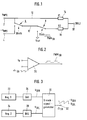
- Fig. 1 shows in schematic form for one of the two channels, here the right channel, the demodulator part used for channel separation.
- the multiplex stereo signal V MPX or -V MPX is fed to two inputs 2 and 4.
- the signal V MPX constantly passes through an unswitched signal path 10 and a resistor 14 (R1) to an output 18 of the demodulator part, which also functions as a summing point.
- the signal -V MPX passes from the input 4 via a first switch 6 to a switched signal path 12.
- the switch 6 is e.g. B. a transistor switch and is switched at a frequency of 38 kHz (corresponding to the carrier frequency) between inputs 2 and 4.
- a further switch 8 is located in the switched signal path 12 and is used for smooth switching between stereo operation and mono operation. Without this switch, the differential signal (LR) reached the output 18 via the resistor 16 (R2).
- the two resistors 14 and 16 determine the ratio with which the two components (L + R) and (LR) are summed at the output 18 .
- switch 8 is controlled with a pulse width signal PWM SB , the pulse duty factor of which is continuously changed between a minimum and a maximum value depending on the reception field strength.
- the minimum value corresponds to a pulse duty factor of "0", ie there are no pulses, so that the switch 8 always remains open.
- the maximum value corresponds to the maximum pulse width, so that the switch 8 is practically always closed.
- FIG. 2 schematically shows a comparator 20, with the aid of which the signal PWM SB (the index SB relates to the term "stereo blend", that is to say the smooth switching between mono operation and stereo operation) is generated.
- the field strength signal V F is applied to one input of the comparator, and a triangular signal ⁇ SB is applied to the other input.
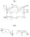
- the generation of the PWM signal is explained in more detail in FIG. 4.
- the field strength signal V F is represented by a dash-dotted line.
- the triangular signal ⁇ SB fluctuates between an upper level V SBH and a lower level V SBL1 or V SBL2 .
- the lower level can be set here, which is indicated by the two alternative lower limit values V SBL1 and V SBL2 .
- the upper limit value V SBH can also be set.
- the time course of the triangular signal can be influenced by changing at least one limit value. If the triangular signal ⁇ SB intersects the field strength signal V F in the negative direction, as is the case at time t 1 , the comparator 20 according to FIG. 2 supplies an increasing pulse.
- the output signal of the comparator drops from a high level to a low level. This creates a pulse train, and depending on how large the level of the signal V F is, relatively long or relatively short pulses are generated.
- the time behavior of the triangular signal changes in such a way that the triangular signal intersects the signal V F at a different point in time, here for example at a point in time t 3 .
- the PWM signal PWM SB also changes , which is shown by the dashed pulse stretching between times t 2 and t 3 in FIG. 4.
- the subsequent pulses of the PWM SB signal also change.
- FIG. 3 shows a block diagram of a triangular signal generator 30 which supplies the triangular signal ⁇ SB at its output 32.
- Triangle signal generators can be designed in different ways. In the present context, it is important that the shape of the triangular signal is changed by specifying the upper and lower threshold values V SBH and V SBL , without however affecting the frequency and the phase position of the triangular signal.
- Two registers 22 and 24 are provided in FIG. 3 (Reg. 1; Reg. 2).
- a digital value is entered in each register via a digital input device, not shown here, and each digital value is converted from the associated register via a digital-to-analog converter 26 or 28 into an analog voltage signal corresponding to the upper threshold value V SBH and the lower threshold value V SBL implemented.
- a capacitor circuit is then continuously charged and discharged so that the triangular signal ⁇ SB obtained at the output 32 is generated.
- the above-described demodulator part shown in FIG. 1, the comparator shown in FIG. 2 and the circuit for generating the triangular signal ⁇ SB shown in FIG. 3 are formed together with numerous other circuit parts on a chip of an integrated circuit.
Landscapes
- Engineering & Computer Science (AREA)
- Signal Processing (AREA)
- Computer Networks & Wireless Communication (AREA)
- Multimedia (AREA)
- Physics & Mathematics (AREA)
- Acoustics & Sound (AREA)
- Stereo-Broadcasting Methods (AREA)
- Stereophonic System (AREA)
Abstract
Description
- Fig. 1
- eine vereinfachte schematische Darstellung eines Teils eines Demodulators für einen der beiden Kanäle;
- Fig. 2
- eine Prinzip-Schaltskizze eines Vergleichers zum Erzeugen eines PWM-Signals;
- Fig. 3
- ein Blockschaltbild eines Dreiecksignalgenerators mit veränderlichen Grenzwert-Spannungen;
- Fig. 4
- eine detaillierte Ansicht eines Dreiecksignals und eines daraus gewonnenen PWM-Signals; und
- Fig. 5
- den hier interessierenden Teil des Spektrums des Eingangssignals des in einem Audiosignalprozessor befindlichen Demodulators.
Claims (4)
- Vorrichtung zum gleitenden Umsteuern eines Demodulators in einem Stereodecoder von Stereobetrieb auf Monobetrieb, und umgekehrt, wozu das Differenzsignal (L-R) des von einem HF-Teil einem Eingang (2, 4) des Demodulators zugeführten Multiplex-Stereosignals (VMPX) mit einem veränderlichen Faktor (k) auf das Summensignal (L+R) des Multiplex-Stereosignals addiert wird, um an zwei Ausgängen getrennte Signale für die beiden Kanäle (L, R) zu erhalten, wobei der Faktor (k) durch einen im Signalweg (12) zwischen dem Eingang (2, 4) und jeweils einem Ausgang liegenden Schalter (8) realisiert wird, der von einem PWM-Signal (PWMSB) angesteuert wird, dessen Tastverhältnis nach Maßgabe eines Feldstärkensignals (VF) verändert wird, wozu dieses Feldstärkensignal (VF) mit einem Referenz-Dreiecksignal verglichen wird, dessen Amplitude sich zwischen einem oberen und einem unteren Grenzwert ändert,
dadurch gekennzeichnet, daß der Stereodecoder mindestens ein Grenzwertspeicherregister (22, 24) aufweist, in das von außerhalb des Audioprozessors ein digitaler Grenzwert eingebbar ist, der in eine Analogspannung (VSBH; VSBL) umgesetzt wird und als Grenzwert einem Dreiecksignalgenerator (30) zugeführt wird. - Vorrichtung nach Anspruch 1,
dadurch gekennzeichnet, daß zwei Register (22, 24) für den oberen bzw. den unteren Grenzwert vorgesehen sind. - Vorrichtung nach Anspruch 1 oder 2,
dadurch gekennzeichnet, daß jedem Grenzwertspeicherregister (22, 24) ein Digital-Analog-Umsetzer (26, 28) zugeordnet ist. - Stereodecoder, gekennzeichnet durch eine Vorrichtung zum gleitenden Umsteuern nach einem der Ansprüche 1 bis 3.
Applications Claiming Priority (2)
| Application Number | Priority Date | Filing Date | Title |
|---|---|---|---|
| DE19630392 | 1996-07-26 | ||
| DE19630392A DE19630392C2 (de) | 1996-07-26 | 1996-07-26 | Stereodecoder mit gleitendem Übergang zwischen Stereobetrieb und Monobetrieb |
Publications (3)
| Publication Number | Publication Date |
|---|---|
| EP0821544A2 true EP0821544A2 (de) | 1998-01-28 |
| EP0821544A3 EP0821544A3 (de) | 2007-02-28 |
| EP0821544B1 EP0821544B1 (de) | 2008-04-23 |
Family
ID=7801053
Family Applications (1)
| Application Number | Title | Priority Date | Filing Date |
|---|---|---|---|
| EP97112875A Expired - Lifetime EP0821544B1 (de) | 1996-07-26 | 1997-07-25 | Vorrichtung zum gleitenden Umsteuern eines Demodulators von Stereobetrieb auf Monobetrieb, und umgekehrt |
Country Status (4)
| Country | Link |
|---|---|
| US (1) | US5920632A (de) |
| EP (1) | EP0821544B1 (de) |
| JP (1) | JPH10229600A (de) |
| DE (1) | DE19630392C2 (de) |
Families Citing this family (5)
| Publication number | Priority date | Publication date | Assignee | Title |
|---|---|---|---|---|
| US7406302B1 (en) * | 2003-12-15 | 2008-07-29 | Marvell International, Inc. | Digital FM stereo receiver architecture |
| US7343080B2 (en) | 2004-09-27 | 2008-03-11 | Idc, Llc | System and method of testing humidity in a sealed MEMS device |
| US7359066B2 (en) * | 2004-09-27 | 2008-04-15 | Idc, Llc | Electro-optical measurement of hysteresis in interferometric modulators |
| JP2006115200A (ja) * | 2004-10-14 | 2006-04-27 | Fujitsu Ten Ltd | 受信機 |
| CN104346645B (zh) * | 2013-07-30 | 2017-03-29 | 上海华虹宏力半导体制造有限公司 | 非接触ic卡的解调电路 |
Family Cites Families (11)
| Publication number | Priority date | Publication date | Assignee | Title |
|---|---|---|---|---|
| DE1233015B (de) * | 1963-08-17 | 1967-01-26 | Loewe Opta Gmbh | HF-Stereo-Decoder mit elektronischer Mono-Stereo-Umschaltung |
| AT289200B (de) * | 1969-05-22 | 1971-04-13 | Philips Nv | Schaltungsanordnung für Stereo-Decoder |
| DE2511026A1 (de) * | 1975-03-13 | 1976-09-16 | Siemens Ag | Schaltungsanordnung zur kontinuierlichen basisbreiteneinstellung in einem stereodecoder |
| US4489431A (en) * | 1982-06-08 | 1984-12-18 | Motorola, Inc. | Signal interference protection circuit for AM stereo receiver |
| JPS61263327A (ja) * | 1985-05-17 | 1986-11-21 | Pioneer Electronic Corp | 音声多重受信機 |
| US4833715A (en) * | 1987-03-06 | 1989-05-23 | Alps Electric Co., Ltd. | FM stereo receiver |
| US4817151A (en) * | 1987-11-09 | 1989-03-28 | Broadcast Technology Partners | Selective decoder for compatible FM stereophonic system utilizing companding of difference signal |
| JP2792857B2 (ja) * | 1988-01-20 | 1998-09-03 | 三洋電機株式会社 | ステレオ復調回路 |
| JPH0429244U (de) * | 1990-07-05 | 1992-03-09 | ||
| JP3006059B2 (ja) * | 1990-09-17 | 2000-02-07 | ソニー株式会社 | 音場拡大装置 |
| US5432854A (en) * | 1993-02-25 | 1995-07-11 | Chrysler Corporation | Stereo FM receiver, noise control circuit therefor |
-
1996
- 1996-07-26 DE DE19630392A patent/DE19630392C2/de not_active Expired - Fee Related
-
1997
- 1997-07-25 US US08/900,608 patent/US5920632A/en not_active Expired - Lifetime
- 1997-07-25 JP JP9199458A patent/JPH10229600A/ja active Pending
- 1997-07-25 EP EP97112875A patent/EP0821544B1/de not_active Expired - Lifetime
Also Published As
| Publication number | Publication date |
|---|---|
| EP0821544B1 (de) | 2008-04-23 |
| DE19630392A1 (de) | 1998-03-19 |
| EP0821544A3 (de) | 2007-02-28 |
| DE19630392C2 (de) | 1998-10-01 |
| US5920632A (en) | 1999-07-06 |
| JPH10229600A (ja) | 1998-08-25 |
Similar Documents
| Publication | Publication Date | Title |
|---|---|---|
| EP0497115B1 (de) | Verfahren zur Überbrückung von Audiosignalunterbrechungen | |
| DE3131292C2 (de) | ||
| DE3939478C2 (de) | Vorrichtung zur Rauschunterdrückung in einem FM-Stereotuner | |
| DE2628737A1 (de) | Fernsehempfaenger mit einer einrichtung zur gleichzeitigen wiedergabe mehrerer programme | |
| DE2305847B2 (de) | Anordnung zum erzeugen einer beliebigen frequenz aus einer anzahl in einem breiten frequenzband liegender diskreter frequenzen | |
| EP0617519B1 (de) | Verfahren zur Ableitung mindestens eines von der Qualität eines empfangenen Signals abhängigen Qualitätssignals | |
| DE19630395C1 (de) | Elektrische Stummsteuerschaltung | |
| DE2711524C2 (de) | Schaltungsanordnung zur Rauschunterdrückung bei einem FM-Empfänger | |
| DE69319777T2 (de) | Mehrwegeempfangsdetektor mit Phasenvergleich des Stereopilotsignales | |
| EP0821544B1 (de) | Vorrichtung zum gleitenden Umsteuern eines Demodulators von Stereobetrieb auf Monobetrieb, und umgekehrt | |
| DE4103061C2 (de) | Rundfunkempfänger | |
| EP0691050B1 (de) | Schaltungsanordnung zur ableitung von signalen zur maskierung von audiosignalen | |
| DE60026179T2 (de) | Fm rundfunkempfänger | |
| DE3009787A1 (de) | Ukw-autoradio mit zwei empfangsteilen und sendersuchlauf | |
| DE3153411C2 (en) | Multi-station receiver with muting circuit | |
| DE3829004A1 (de) | Rundfunkempfaenger | |
| DE2659447C3 (de) | Für ein Kraftfahrzeug vorgesehener Rundfunkempfänger | |
| DE3925629A1 (de) | Verfahren zum erfassen von mehrwegeverzerrungen beim fm-rundfunkempfang und schaltungsanordnung zur durchfuehrung des verfahrens | |
| EP0046835A2 (de) | Vielkanal-Sprechfunkgerät für die Betriebsarten 'Wechselsprechen' und/oder 'bedingtes Gegensprechen' | |
| DE3521099C2 (de) | ||
| DE2928367C2 (de) | Mehrkanal-Signalverarbeitungsschaltung in integrierter Bauweise | |
| EP0082381B1 (de) | Elektronischer Verstärker | |
| DE2633000A1 (de) | Rundfunkempfaenger mit stoerimpulsaustastung | |
| DE3007632A1 (de) | Schaltungsanordnung zur rueckkopplungsverhinderung bei telefonapparaten mit freisprech- und/oder mithoermoeglichkeit | |
| DE2926137C2 (de) | Demodulationsschaltung für stereophone Signale |
Legal Events
| Date | Code | Title | Description |
|---|---|---|---|
| PUAI | Public reference made under article 153(3) epc to a published international application that has entered the european phase |
Free format text: ORIGINAL CODE: 0009012 |
|
| AK | Designated contracting states |
Kind code of ref document: A2 Designated state(s): AT BE CH DE DK ES FI FR GB GR IE IT LI LU MC NL PT SE |
|
| PUAL | Search report despatched |
Free format text: ORIGINAL CODE: 0009013 |
|
| AK | Designated contracting states |
Kind code of ref document: A3 Designated state(s): AT BE CH DE DK ES FI FR GB GR IE IT LI LU MC NL PT SE |
|
| RIC1 | Information provided on ipc code assigned before grant |
Ipc: H04H 5/00 20060101ALI20070124BHEP Ipc: H04S 1/00 20060101AFI19971121BHEP |
|
| 17P | Request for examination filed |
Effective date: 20070823 |
|
| AKX | Designation fees paid |
Designated state(s): FR GB IT |
|
| GRAP | Despatch of communication of intention to grant a patent |
Free format text: ORIGINAL CODE: EPIDOSNIGR1 |
|
| REG | Reference to a national code |
Ref country code: DE Ref legal event code: 8566 |
|
| GRAS | Grant fee paid |
Free format text: ORIGINAL CODE: EPIDOSNIGR3 |
|
| GRAA | (expected) grant |
Free format text: ORIGINAL CODE: 0009210 |
|
| AK | Designated contracting states |
Kind code of ref document: B1 Designated state(s): FR GB IT |
|
| REG | Reference to a national code |
Ref country code: GB Ref legal event code: FG4D Free format text: NOT ENGLISH |
|
| EN | Fr: translation not filed | ||
| PLBE | No opposition filed within time limit |
Free format text: ORIGINAL CODE: 0009261 |
|
| STAA | Information on the status of an ep patent application or granted ep patent |
Free format text: STATUS: NO OPPOSITION FILED WITHIN TIME LIMIT |
|
| GBPC | Gb: european patent ceased through non-payment of renewal fee |
Effective date: 20080725 |
|
| 26N | No opposition filed |
Effective date: 20090126 |
|
| PG25 | Lapsed in a contracting state [announced via postgrant information from national office to epo] |
Ref country code: GB Free format text: LAPSE BECAUSE OF NON-PAYMENT OF DUE FEES Effective date: 20080725 |
|
| PG25 | Lapsed in a contracting state [announced via postgrant information from national office to epo] |
Ref country code: IT Free format text: LAPSE BECAUSE OF NON-PAYMENT OF DUE FEES Effective date: 20080725 |
|
| PG25 | Lapsed in a contracting state [announced via postgrant information from national office to epo] |
Ref country code: FR Free format text: LAPSE BECAUSE OF FAILURE TO SUBMIT A TRANSLATION OF THE DESCRIPTION OR TO PAY THE FEE WITHIN THE PRESCRIBED TIME-LIMIT Effective date: 20090227 |