EP0821832B1 - Kompakte mikrowellen lampe - Google Patents
Kompakte mikrowellen lampe Download PDFInfo
- Publication number
- EP0821832B1 EP0821832B1 EP96913001A EP96913001A EP0821832B1 EP 0821832 B1 EP0821832 B1 EP 0821832B1 EP 96913001 A EP96913001 A EP 96913001A EP 96913001 A EP96913001 A EP 96913001A EP 0821832 B1 EP0821832 B1 EP 0821832B1
- Authority
- EP
- European Patent Office
- Prior art keywords
- waveguide
- slot
- lamp
- magnetron
- recited
- Prior art date
- Legal status (The legal status is an assumption and is not a legal conclusion. Google has not performed a legal analysis and makes no representation as to the accuracy of the status listed.)
- Expired - Lifetime
Links
- 230000008878 coupling Effects 0.000 claims abstract description 14
- 238000010168 coupling process Methods 0.000 claims abstract description 14
- 238000005859 coupling reaction Methods 0.000 claims abstract description 14
- 239000010445 mica Substances 0.000 claims description 2
- 229910052618 mica group Inorganic materials 0.000 claims description 2
- 239000010453 quartz Substances 0.000 description 4
- VYPSYNLAJGMNEJ-UHFFFAOYSA-N silicon dioxide Inorganic materials O=[Si]=O VYPSYNLAJGMNEJ-UHFFFAOYSA-N 0.000 description 4
- 239000003990 capacitor Substances 0.000 description 3
- BUGBHKTXTAQXES-UHFFFAOYSA-N Selenium Chemical compound [Se] BUGBHKTXTAQXES-UHFFFAOYSA-N 0.000 description 2
- NINIDFKCEFEMDL-UHFFFAOYSA-N Sulfur Chemical compound [S] NINIDFKCEFEMDL-UHFFFAOYSA-N 0.000 description 2
- 238000001816 cooling Methods 0.000 description 2
- 238000005286 illumination Methods 0.000 description 2
- 230000001939 inductive effect Effects 0.000 description 2
- 239000002184 metal Substances 0.000 description 2
- 229910052711 selenium Inorganic materials 0.000 description 2
- 239000011669 selenium Substances 0.000 description 2
- 229910052717 sulfur Inorganic materials 0.000 description 2
- 239000011593 sulfur Substances 0.000 description 2
- 230000000694 effects Effects 0.000 description 1
- 239000011521 glass Substances 0.000 description 1
- 238000009413 insulation Methods 0.000 description 1
- 230000010363 phase shift Effects 0.000 description 1
- 230000001902 propagating effect Effects 0.000 description 1
- 230000005855 radiation Effects 0.000 description 1
- 230000000284 resting effect Effects 0.000 description 1
- 230000008054 signal transmission Effects 0.000 description 1
- 239000002023 wood Substances 0.000 description 1
Images


Classifications
-
- H—ELECTRICITY
- H01—ELECTRIC ELEMENTS
- H01J—ELECTRIC DISCHARGE TUBES OR DISCHARGE LAMPS
- H01J65/00—Lamps without any electrode inside the vessel; Lamps with at least one main electrode outside the vessel
- H01J65/04—Lamps in which a gas filling is excited to luminesce by an external electromagnetic field or by external corpuscular radiation, e.g. for indicating plasma display panels
- H01J65/042—Lamps in which a gas filling is excited to luminesce by an external electromagnetic field or by external corpuscular radiation, e.g. for indicating plasma display panels by an external electromagnetic field
- H01J65/044—Lamps in which a gas filling is excited to luminesce by an external electromagnetic field or by external corpuscular radiation, e.g. for indicating plasma display panels by an external electromagnetic field the field being produced by a separate microwave unit
-
- H—ELECTRICITY
- H01—ELECTRIC ELEMENTS
- H01J—ELECTRIC DISCHARGE TUBES OR DISCHARGE LAMPS
- H01J65/00—Lamps without any electrode inside the vessel; Lamps with at least one main electrode outside the vessel
- H01J65/04—Lamps in which a gas filling is excited to luminesce by an external electromagnetic field or by external corpuscular radiation, e.g. for indicating plasma display panels
Definitions
- the present invention relates to a microwave powered lamp, and particularly to a lamp of the type defined in the precharacterizing portion of claim 1.
- Such microwave lamps may be used as illumination sources, which find a particular use in commercial or industrial lighting.
- These parts include a quartz bulb to contain the arc plasma housed within a microwave cavity having a metal mesh to contain the microwaves but allow the escape of light, a magnetron to produce the microwaves, a waveguide to carry the microwaves from the magnetron to the cavity, a power supply to drive the magnetron and cooling fans or other means to cool the magnetron and its power supply.
- the lamp bulb is rotated within the microwave cavity to stabilize the discharge which adds a motor to the system as well.
- the lamp itself does not include a reflector. Rather the lamp is to be inserted through a hole in reflectors of several designs, suitable for use in applications requiring light dispersal over different areas. This requires the light source to extend outward from the lamp case a distance of at least 100 mm. Keeping the entry hole to a small diameter increases the efficiency of the reflector.
- the bulb stem is fed through the coupling slot and the waveguide, and the motor and coupler are located on the other side of the waveguide, resulting in a very long stem which is subject to breakage.
- a further problem is encountered in that the waveguide must have a sufficiently narrow width so that the cutoff frequency is high enough to eliminate spurious interference signals from being generated, but must have a height sufficient to prevent arcing at the location of the magnetron antenna.
- a conventional WR-284 waveguide is narrow enough to eliminate interference signals, but because of its height which correlates to its width in a conventional ratio of about 1 to 2, arcing results.
- EP-A-0 153 745 discloses various microwave discharge lamp configurations. A conventional waveguide cross-section of 95 mm x 54 mm is disclosed.
- U.S. Patent No. 4,903,935 discloses a microwave discharge lamp utilizing a tilted rotating bulb.
- an electrodeless lamp of the type mentioned above comprises the features of the characterizing portion of claim 1.
- the lamp is comprised of bulb 2 which is located in a microwave cavity.
- the bulb may be made of quartz and encloses a discharge forming medium, for example, a sulfur or selenium based fill.
- the microwave cavity is cylindrical, and is comprised of a side wall structure, and two end walls.
- the side wall structure and top end wall in the orientation of Figure 1 are made of a cylindrical metallic mesh, shown in part at reference numeral 3, which allows light to exit but is substantially opaque to microwave radiation.
- the bottom end wall of the cavity in the orientation of Figure 1 is the outside surface 8 of waveguide 10.
- the microwave lamp depicted in Figure 1 may be used to replace existing non-microwave lamps, and it is therefore desirable for the lamp to be made as compact as possible so as to fit within the general outline of existing lamps.
- the bulb stem In some microwave lamps of the prior art wherein the bulb stem extends from an end wall, it passes through the waveguide which feeds the cavity, and the motor and coupling ferrule are mounted on the opposite side of the waveguide, far enough away to be clear of microwave fields. Such an arrangement, however, may have the effect of increasing the overall length of the lamp, as well as the length of the bulb stem, thereby making it subject to breakage.
- the coupling slot is located to one side of center in the cavity end wall, while the bulb stem is fed through the end wall to the other side of center canted in relation to the end wall, with the motor and ferrule being mounted outside the cavity and away from the waveguide.
- the longitudinal direction of the waveguide extends parallel to the end wall of the cavity, so as to not extend the length of the lamp. The result is a more compact lamp of shorter overall length, wherein the bulb is more ruggedly supported on a shorter stem.
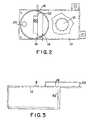
- rectangular waveguide 10 is shown, having inside wall 12 and outside wall 8 (see Fig. 1).
- the top walls of the waveguide have coupling slot 14 therein, which is shown in Figure 2.
- end wall 16 of the waveguide is slightly wider than the coupling slot 14.
- magnetron 18 having antenna 20 is mounted to the waveguide, as shown.
- Microwave power is fed into the waveguide and through coupling slot 14 (see Fig. 2) to the microwave cavity, where it excites the fill in bulb 2.
- hole 21 is shown, through which the magnetron antenna and a gasket protrude.
- bulb stem 22 is passed through hole 24 at an angle of other than 90°, (about 77° in the preferred embodiment) so that the bulb is centrally located in relation to the mesh side wall structure of the cavity.
- the motor 26 is mounted to motor support 28, while ferrule 30 couples the motor shaft to the bulb stem, which is typically made of quartz.
- Extension 34 of support 28 is secured to the bottom outside surface of the waveguide, while gap 36 is present between the motor support and the end wall of the waveguide.
- top wall 8 of the waveguide extends to the left at reference numeral 40 past the end of the waveguide. Additionally, the top of the waveguide is flush against plate 32, which is secured to plate 42 at the ends thereof with flanges 44 and 46.
- metallic ring 52 is mounted on the top surface of the waveguide (cavity end). The cylindrical mesh is secured to this ring by a clamp, and the mesh passes through a hole in plate 42.
- a transparent cylindrical envelope 54 which may be made of glass or quartz surrounds the screen, and is mounted on plate 42, for example by retainer 56. Thermal insulation is disposed in the space between plates 32 and 42.
- microwave power generated by the magnetron is fed through the waveguide and the coupling slot into the cavity in which bulb 2 is located.
- magnetron antenna 20 is located 1/4 guide wavelength (the wavelength of signals propagating within the waveguide) from coupling slot 14.
- a waveguide having a width sufficiently narrow to have a cut-off frequency sufficiently high to eliminate spurious signals was necessary.
- a waveguide was tried which accommodated the magnetron antenna produced out of band signals 200 Mhz below the normal operation point of 2450 Mhz, and the use of the 1/4 wavelength waveguide length referred to above tends to aggravate this situation.
- a WR-284 (equivalent IEC designation, R-32) waveguide was sufficiently narrow to eliminate spurious signals, but it was found that the height of this waveguide, which is 3.404 cm (1.340 in.), was too small to accommodate the magnetron antenna without arcing.
- a non-conventional waveguide was used having about the width of the WR-284 waveguide, which is 7.214 cm (2.840 in.), and about the height of the WR-340 (equivalent IEC designation, R-26) waveguide, which is 4.318 cm (1.700 in.).
- This blocks the transmission of signals below 2078 Mhz and helps to suppress the low frequency out of band signals by reducing the phase shift between the magnetron and the coupling slot.
- the height of the waveguide is sufficient to accommodate the magnetron antenna without arcing.
- EIA Electronics Industry Association
- the waveguide end wall behind the magnetron is moved farther away than is the usual practice.
- a metal tuning knob was used to match the impedance of the lamp to the waveguide. This knob functioned as a capacitor at its location. With the length reduction to one quarter wavelength, this position became the same as the magnetron antenna.
- a tuning knob might have been placed beside the antenna, taking care to avoid arcing, however, the magnetron antenna itself is a capacitor across the waveguide. This is usually compensated by placing the end wall in an inductive position, closer to the antenna than a quarter wavelength. By moving the wall farther out, the inductance is reduced and the antenna is seen as the desired tuning capacitance. The best position was found experimentally by using a movable waveguide end wall.
- matching is accomplished by placing a tuning knob in the waveguide. If all possible load phases are to be corrected, a half-wavelength of waveguide is needed. According to the invention, the system was matched by placing a thin block 60, shown in Figure 2, beside the slot 14 to modify the current path.
- dielectric member 62 which may be made of mica is depicted. This member rests against the inside end wall of the waveguide and protrudes through coupling slot 14 while resting against the edge of the slot. It may be substantially as wide as the slot. The purpose of member 62 is to prevent arcing across the slot.
- Figure 4 is a plan view of the magnetron and associated components, which are located on plate 32 shown in Figure 1.
- Magnetron 18 receives filament power from filament transformer 70, while stepdown transformer 72 may be used to provide power for bulb rotator motor 26, shown in connection with motor mount 28 and capacitor 74.
- magnetron cooling air blower 76 is depicted as is PC control board 78.
- waveguide 10 is shown feeding coupling slot 14.
Landscapes
- Physics & Mathematics (AREA)
- Engineering & Computer Science (AREA)
- Plasma & Fusion (AREA)
- Electromagnetism (AREA)
- Discharge Lamps And Accessories Thereof (AREA)
- Constitution Of High-Frequency Heating (AREA)
- Circuit Arrangements For Discharge Lamps (AREA)
- Vessels And Coating Films For Discharge Lamps (AREA)
- Non-Portable Lighting Devices Or Systems Thereof (AREA)
Claims (9)
- Kompakte, elektrodenlose Lampe, die folgendes umfaßt:dadurch gekennzeichnet, daß der Abstand zwischen der Antenne (20) und dem Schlitz (14) etwa 1/4 der Wellenlänge des Wellenleiters beträgt und die Breite des Wellenleiters (10) gleich der Breite eines Wellenleiters WR-284 ist, und daß die Höhe des Wellenleiters (10) gleich der Höhe eines Wellenleiters WR-340 ist.einen Mikrowellenhohlraum;einen in dem Mikrowellenhohlraum angeordneten Kolben (2), wobei der Kolben (2) eine eine Entladung erzeugende Füllung enthält;ein Magnetron (18) zur Bereitstellung von Mikrowellenleistung bei 2450 MHz, wobei das Magnetron eine Antenne (20) hat;einen Wellenleiter (10), der mit dem Magnetron (18) verbunden ist, so daß sich die Antenne (20) des Magnetrons (18) im Inneren des Wellenleiters (10) und parallel zu einer Höhenabmessung des Wellenleiters (10) erstreckt, wobei der Wellenleiter (10) einen Schlitz (14) in einer Wand (8, 12) des Wellenleiters (10) umfaßt, um die Mikrowellenleistung an den Mikrowellenhohlraum zu koppeln,
- Elektrodenlose Lampe nach Anspruch 1, die ferner einen im Inneren des Mikrowellenhohlraums angrenzend an den Schlitz (14) positionierten Block (60) umfaßt.
- Elektrodenlose Lampe nach Anspruch 2, bei der der Block (60) dünn ist.
- Elektrodenlose Lampe nach Anspruch 2, bei der der Block (60) ein feststehendes metallisches Abstimmelement umfaßt.
- Elektrodenlose Lampe nach Anspruch 1, die ferner ein dielektrisches Element (62) umfaßt, das an einer Wand des Schlitzes (14) positioniert ist und sich in den Mikrowellenhohlraum erstreckt.
- Elektrodenlose Lampe nach Anspruch 5, bei der das dielektrische Element (62) aus Glimmer besteht.
- Elektrodenlose Lampe nach Anspruch 5, bei der sich das dielektrische Element (62) durch den Schlitz (14) erstreckt.
- Elektrodenlose Lampe nach Anspruch 5, bei der das dielektrische Element (62) im wesentlichen so breit wie der Schlitz (14) ist.
- Elektrodenlose Lampe nach Anspruch 5, bei der eine Stirnwand (16) des Wellenleiters (10) im wesentlichen mit der Wand des Schlitzes (14) fluchtet, und bei der sich das dielektrische Element (62) durch den Schlitz (14) erstreckt und an der Stirnwand (16) des Wellenleiters (10) positioniert ist.
Applications Claiming Priority (3)
| Application Number | Priority Date | Filing Date | Title |
|---|---|---|---|
| US42660395A | 1995-04-21 | 1995-04-21 | |
| US426603 | 1995-04-21 | ||
| PCT/US1996/005556 WO1996033509A1 (en) | 1995-04-21 | 1996-04-22 | Compact microwave lamp |
Publications (2)
| Publication Number | Publication Date |
|---|---|
| EP0821832A1 EP0821832A1 (de) | 1998-02-04 |
| EP0821832B1 true EP0821832B1 (de) | 2002-10-23 |
Family
ID=23691463
Family Applications (1)
| Application Number | Title | Priority Date | Filing Date |
|---|---|---|---|
| EP96913001A Expired - Lifetime EP0821832B1 (de) | 1995-04-21 | 1996-04-22 | Kompakte mikrowellen lampe |
Country Status (11)
| Country | Link |
|---|---|
| EP (1) | EP0821832B1 (de) |
| JP (1) | JPH11511892A (de) |
| KR (1) | KR19990007961A (de) |
| AT (1) | ATE226759T1 (de) |
| AU (1) | AU5563796A (de) |
| CA (1) | CA2218500A1 (de) |
| DE (1) | DE69624472D1 (de) |
| HU (1) | HUP9802761A3 (de) |
| IL (1) | IL117972A (de) |
| WO (1) | WO1996033509A1 (de) |
| ZA (1) | ZA963179B (de) |
Families Citing this family (10)
| Publication number | Priority date | Publication date | Assignee | Title |
|---|---|---|---|---|
| TW406280B (en) | 1997-05-21 | 2000-09-21 | Fusion Lighting Inc | non-rotating electrodeless lamp containing molecular fill |
| KR100724371B1 (ko) * | 2000-12-27 | 2007-06-04 | 엘지전자 주식회사 | 마이크로파를 이용한 조명 장치 |
| KR100442374B1 (ko) * | 2001-07-20 | 2004-07-30 | 엘지전자 주식회사 | 마이크로파를 이용한 조명시스템 |
| KR100430013B1 (ko) * | 2002-05-16 | 2004-05-03 | 엘지전자 주식회사 | 무전극 램프의 무전극 전구 체결장치 |
| KR100430012B1 (ko) * | 2002-05-16 | 2004-05-03 | 엘지전자 주식회사 | 무전극 램프의 열변형 방지장치 |
| KR101241049B1 (ko) | 2011-08-01 | 2013-03-15 | 주식회사 플라즈마트 | 플라즈마 발생 장치 및 플라즈마 발생 방법 |
| KR101246191B1 (ko) | 2011-10-13 | 2013-03-21 | 주식회사 윈텔 | 플라즈마 장치 및 기판 처리 장치 |
| KR101332337B1 (ko) | 2012-06-29 | 2013-11-22 | 태원전기산업 (주) | 초고주파 발광 램프 장치 |
| KR101891869B1 (ko) * | 2015-12-31 | 2018-08-24 | 엘지전자 주식회사 | 무전극 플라즈마 조명기기 |
| KR102136592B1 (ko) * | 2016-04-29 | 2020-07-22 | (주)디앤지라이텍 | 무전극 플라즈마 조명장치 |
Family Cites Families (6)
| Publication number | Priority date | Publication date | Assignee | Title |
|---|---|---|---|---|
| US4189661A (en) * | 1978-11-13 | 1980-02-19 | Gte Laboratories Incorporated | Electrodeless fluorescent light source |
| AU574435B2 (en) * | 1984-03-02 | 1988-07-07 | Mitsubishi Denki Kabushiki Kaisha | Microwave discharge light source apparatus |
| DE69125499T2 (de) * | 1990-10-25 | 1997-07-17 | Fusion Systems Corp., Rockville, Md. | Hochleistungslampe |
| HU217160B (hu) * | 1990-10-25 | 1999-11-29 | Fusion Lighting Inc. | Gázkisülő lámpa, továbbá eljárás gázkisülő lámpa készítésére, valamint annak működtetésére |
| US5227698A (en) * | 1992-03-12 | 1993-07-13 | Fusion Systems Corporation | Microwave lamp with rotating field |
| KR960030307A (ko) * | 1995-01-28 | 1996-08-17 | 켄트 키플링 | 전자기파를 무전극 램프에 커플링하기 위한 장치 |
-
1996
- 1996-04-18 IL IL11797296A patent/IL117972A/xx not_active IP Right Cessation
- 1996-04-22 JP JP8531981A patent/JPH11511892A/ja active Pending
- 1996-04-22 WO PCT/US1996/005556 patent/WO1996033509A1/en not_active Ceased
- 1996-04-22 AT AT96913001T patent/ATE226759T1/de not_active IP Right Cessation
- 1996-04-22 CA CA002218500A patent/CA2218500A1/en not_active Abandoned
- 1996-04-22 ZA ZA963179A patent/ZA963179B/xx unknown
- 1996-04-22 EP EP96913001A patent/EP0821832B1/de not_active Expired - Lifetime
- 1996-04-22 AU AU55637/96A patent/AU5563796A/en not_active Abandoned
- 1996-04-22 DE DE69624472T patent/DE69624472D1/de not_active Expired - Lifetime
- 1996-04-22 HU HU9802761A patent/HUP9802761A3/hu unknown
- 1996-04-22 KR KR1019970707485A patent/KR19990007961A/ko not_active Ceased
Non-Patent Citations (1)
| Title |
|---|
| PEHL E.: "Mikrowellentechnik, Bd. 1", 1988, HÜTHIG, HEIDELBERG * |
Also Published As
| Publication number | Publication date |
|---|---|
| AU5563796A (en) | 1996-11-07 |
| JPH11511892A (ja) | 1999-10-12 |
| IL117972A (en) | 1999-06-20 |
| WO1996033509A1 (en) | 1996-10-24 |
| IL117972A0 (en) | 1996-08-04 |
| DE69624472D1 (de) | 2002-11-28 |
| CA2218500A1 (en) | 1996-10-24 |
| KR19990007961A (ko) | 1999-01-25 |
| HUP9802761A2 (hu) | 1999-03-29 |
| EP0821832A1 (de) | 1998-02-04 |
| ATE226759T1 (de) | 2002-11-15 |
| ZA963179B (en) | 1996-11-11 |
| MX9708082A (es) | 1998-07-31 |
| HUP9802761A3 (en) | 2000-09-28 |
Similar Documents
| Publication | Publication Date | Title |
|---|---|---|
| US6031333A (en) | Compact microwave lamp having a tuning block and a dielectric located in a lamp cavity | |
| US4042850A (en) | Microwave generated radiation apparatus | |
| US8110988B2 (en) | Plasma lamp with dielectric waveguide | |
| US5834895A (en) | Visible lamp including selenium | |
| US5070277A (en) | Electrodless hid lamp with microwave power coupler | |
| EP0840354A2 (de) | Energieversorgungsvorrichtung einer Hochfrequenzentladung und elektrodenlose Hochfrequenz-Entladungslampenvorrichtung | |
| CN102356449A (zh) | 低频无电极等离子体灯 | |
| EP0821832B1 (de) | Kompakte mikrowellen lampe | |
| EP0988639A2 (de) | Elektrodenlose lampe mit molekularer füllung | |
| EP0457242B1 (de) | Elektrodenlose Entladungslampe höherer Intensität mit Koppler für ihren Anschluss an einen Mikrowellengenerator | |
| KR19990081919A (ko) | 무선주파 전력으로 구동되는 무전극 램프 | |
| EP0749152B1 (de) | Elektrodenlose Starkstromentladungslampe mit Hilfsmittel zur Feldsymmetrierung | |
| US9805925B1 (en) | Electrodeless high intensity discharge lamp with field suppression probes | |
| EP0321792A2 (de) | Mikrowellenresonanz Hohlraum | |
| MXPA97008082A (en) | Compact microon lamp | |
| KR100517924B1 (ko) | 무전극 램프 시스템의 발광 촉진 장치 | |
| HK1010276A (en) | High frequency discharge energy supply means and high frequency electrodeless discharge lamp device |
Legal Events
| Date | Code | Title | Description |
|---|---|---|---|
| PUAI | Public reference made under article 153(3) epc to a published international application that has entered the european phase |
Free format text: ORIGINAL CODE: 0009012 |
|
| 17P | Request for examination filed |
Effective date: 19971118 |
|
| AK | Designated contracting states |
Kind code of ref document: A1 Designated state(s): AT BE CH DE DK ES FI FR GB GR IE IT LI NL PT SE |
|
| 17Q | First examination report despatched |
Effective date: 19981222 |
|
| GRAG | Despatch of communication of intention to grant |
Free format text: ORIGINAL CODE: EPIDOS AGRA |
|
| GRAG | Despatch of communication of intention to grant |
Free format text: ORIGINAL CODE: EPIDOS AGRA |
|
| GRAH | Despatch of communication of intention to grant a patent |
Free format text: ORIGINAL CODE: EPIDOS IGRA |
|
| GRAH | Despatch of communication of intention to grant a patent |
Free format text: ORIGINAL CODE: EPIDOS IGRA |
|
| GRAA | (expected) grant |
Free format text: ORIGINAL CODE: 0009210 |
|
| AK | Designated contracting states |
Kind code of ref document: B1 Designated state(s): AT BE CH DE DK ES FI FR GB GR IE IT LI NL PT SE |
|
| PG25 | Lapsed in a contracting state [announced via postgrant information from national office to epo] |
Ref country code: NL Free format text: LAPSE BECAUSE OF FAILURE TO SUBMIT A TRANSLATION OF THE DESCRIPTION OR TO PAY THE FEE WITHIN THE PRESCRIBED TIME-LIMIT Effective date: 20021023 Ref country code: LI Free format text: LAPSE BECAUSE OF FAILURE TO SUBMIT A TRANSLATION OF THE DESCRIPTION OR TO PAY THE FEE WITHIN THE PRESCRIBED TIME-LIMIT Effective date: 20021023 Ref country code: IT Free format text: LAPSE BECAUSE OF FAILURE TO SUBMIT A TRANSLATION OF THE DESCRIPTION OR TO PAY THE FEE WITHIN THE PRESCRIBED TIME-LIMIT;WARNING: LAPSES OF ITALIAN PATENTS WITH EFFECTIVE DATE BEFORE 2007 MAY HAVE OCCURRED AT ANY TIME BEFORE 2007. THE CORRECT EFFECTIVE DATE MAY BE DIFFERENT FROM THE ONE RECORDED. Effective date: 20021023 Ref country code: GR Free format text: LAPSE BECAUSE OF FAILURE TO SUBMIT A TRANSLATION OF THE DESCRIPTION OR TO PAY THE FEE WITHIN THE PRESCRIBED TIME-LIMIT Effective date: 20021023 Ref country code: FR Free format text: LAPSE BECAUSE OF FAILURE TO SUBMIT A TRANSLATION OF THE DESCRIPTION OR TO PAY THE FEE WITHIN THE PRESCRIBED TIME-LIMIT Effective date: 20021023 Ref country code: FI Free format text: LAPSE BECAUSE OF FAILURE TO SUBMIT A TRANSLATION OF THE DESCRIPTION OR TO PAY THE FEE WITHIN THE PRESCRIBED TIME-LIMIT Effective date: 20021023 Ref country code: CH Free format text: LAPSE BECAUSE OF FAILURE TO SUBMIT A TRANSLATION OF THE DESCRIPTION OR TO PAY THE FEE WITHIN THE PRESCRIBED TIME-LIMIT Effective date: 20021023 Ref country code: BE Free format text: LAPSE BECAUSE OF FAILURE TO SUBMIT A TRANSLATION OF THE DESCRIPTION OR TO PAY THE FEE WITHIN THE PRESCRIBED TIME-LIMIT Effective date: 20021023 Ref country code: AT Free format text: LAPSE BECAUSE OF FAILURE TO SUBMIT A TRANSLATION OF THE DESCRIPTION OR TO PAY THE FEE WITHIN THE PRESCRIBED TIME-LIMIT Effective date: 20021023 |
|
| REF | Corresponds to: |
Ref document number: 226759 Country of ref document: AT Date of ref document: 20021115 Kind code of ref document: T |
|
| REG | Reference to a national code |
Ref country code: GB Ref legal event code: FG4D |
|
| REG | Reference to a national code |
Ref country code: CH Ref legal event code: EP |
|
| REG | Reference to a national code |
Ref country code: IE Ref legal event code: FG4D |
|
| REF | Corresponds to: |
Ref document number: 69624472 Country of ref document: DE Date of ref document: 20021128 |
|
| PG25 | Lapsed in a contracting state [announced via postgrant information from national office to epo] |
Ref country code: SE Free format text: LAPSE BECAUSE OF FAILURE TO SUBMIT A TRANSLATION OF THE DESCRIPTION OR TO PAY THE FEE WITHIN THE PRESCRIBED TIME-LIMIT Effective date: 20030123 Ref country code: PT Free format text: LAPSE BECAUSE OF FAILURE TO SUBMIT A TRANSLATION OF THE DESCRIPTION OR TO PAY THE FEE WITHIN THE PRESCRIBED TIME-LIMIT Effective date: 20030123 Ref country code: DK Free format text: LAPSE BECAUSE OF FAILURE TO SUBMIT A TRANSLATION OF THE DESCRIPTION OR TO PAY THE FEE WITHIN THE PRESCRIBED TIME-LIMIT Effective date: 20030123 |
|
| PG25 | Lapsed in a contracting state [announced via postgrant information from national office to epo] |
Ref country code: DE Free format text: LAPSE BECAUSE OF FAILURE TO SUBMIT A TRANSLATION OF THE DESCRIPTION OR TO PAY THE FEE WITHIN THE PRESCRIBED TIME-LIMIT Effective date: 20030124 |
|
| NLV1 | Nl: lapsed or annulled due to failure to fulfill the requirements of art. 29p and 29m of the patents act | ||
| PG25 | Lapsed in a contracting state [announced via postgrant information from national office to epo] |
Ref country code: IE Free format text: LAPSE BECAUSE OF NON-PAYMENT OF DUE FEES Effective date: 20030422 Ref country code: GB Free format text: LAPSE BECAUSE OF NON-PAYMENT OF DUE FEES Effective date: 20030422 |
|
| PG25 | Lapsed in a contracting state [announced via postgrant information from national office to epo] |
Ref country code: ES Free format text: LAPSE BECAUSE OF FAILURE TO SUBMIT A TRANSLATION OF THE DESCRIPTION OR TO PAY THE FEE WITHIN THE PRESCRIBED TIME-LIMIT Effective date: 20030429 |
|
| REG | Reference to a national code |
Ref country code: CH Ref legal event code: PL |
|
| EN | Fr: translation not filed | ||
| PLBE | No opposition filed within time limit |
Free format text: ORIGINAL CODE: 0009261 |
|
| STAA | Information on the status of an ep patent application or granted ep patent |
Free format text: STATUS: NO OPPOSITION FILED WITHIN TIME LIMIT |
|
| 26N | No opposition filed |
Effective date: 20030724 |
|
| GBPC | Gb: european patent ceased through non-payment of renewal fee |
Effective date: 20030422 |
|
| REG | Reference to a national code |
Ref country code: IE Ref legal event code: MM4A |