EP0822268B1 - Verfahren zur Erzeugung einer haftenden Diamantbeschichtung - Google Patents
Verfahren zur Erzeugung einer haftenden Diamantbeschichtung Download PDFInfo
- Publication number
- EP0822268B1 EP0822268B1 EP96112277A EP96112277A EP0822268B1 EP 0822268 B1 EP0822268 B1 EP 0822268B1 EP 96112277 A EP96112277 A EP 96112277A EP 96112277 A EP96112277 A EP 96112277A EP 0822268 B1 EP0822268 B1 EP 0822268B1
- Authority
- EP
- European Patent Office
- Prior art keywords
- diamond
- substrate
- film
- plasma
- deposition
- Prior art date
- Legal status (The legal status is an assumption and is not a legal conclusion. Google has not performed a legal analysis and makes no representation as to the accuracy of the status listed.)
- Expired - Lifetime
Links
- 229910003460 diamond Inorganic materials 0.000 title claims description 117
- 239000010432 diamond Substances 0.000 title claims description 117
- 238000000151 deposition Methods 0.000 title claims description 40
- 238000000034 method Methods 0.000 title claims description 30
- 239000010409 thin film Substances 0.000 title claims description 12
- 230000001464 adherent effect Effects 0.000 title claims description 10
- 239000000758 substrate Substances 0.000 claims description 79
- 230000008021 deposition Effects 0.000 claims description 38
- 239000011521 glass Substances 0.000 claims description 30
- VNWKTOKETHGBQD-UHFFFAOYSA-N methane Chemical compound C VNWKTOKETHGBQD-UHFFFAOYSA-N 0.000 claims description 27
- CURLTUGMZLYLDI-UHFFFAOYSA-N Carbon dioxide Chemical compound O=C=O CURLTUGMZLYLDI-UHFFFAOYSA-N 0.000 claims description 22
- XUIMIQQOPSSXEZ-UHFFFAOYSA-N Silicon Chemical compound [Si] XUIMIQQOPSSXEZ-UHFFFAOYSA-N 0.000 claims description 20
- 239000010703 silicon Substances 0.000 claims description 20
- 229910052710 silicon Inorganic materials 0.000 claims description 20
- 229920002120 photoresistant polymer Polymers 0.000 claims description 14
- 239000001257 hydrogen Substances 0.000 claims description 13
- 229910052739 hydrogen Inorganic materials 0.000 claims description 13
- 239000007789 gas Substances 0.000 claims description 12
- 239000002245 particle Substances 0.000 claims description 12
- 229910002092 carbon dioxide Inorganic materials 0.000 claims description 11
- 239000001569 carbon dioxide Substances 0.000 claims description 11
- 238000005229 chemical vapour deposition Methods 0.000 claims description 11
- 150000002431 hydrogen Chemical class 0.000 claims description 9
- 239000000203 mixture Substances 0.000 claims description 7
- 239000005388 borosilicate glass Substances 0.000 claims description 5
- UFHFLCQGNIYNRP-UHFFFAOYSA-N Hydrogen Chemical compound [H][H] UFHFLCQGNIYNRP-UHFFFAOYSA-N 0.000 claims description 4
- 239000010408 film Substances 0.000 description 92
- 230000003287 optical effect Effects 0.000 description 24
- 235000012431 wafers Nutrition 0.000 description 21
- 230000005540 biological transmission Effects 0.000 description 15
- 239000000843 powder Substances 0.000 description 12
- 238000012360 testing method Methods 0.000 description 12
- 239000000463 material Substances 0.000 description 11
- 229910052782 aluminium Inorganic materials 0.000 description 9
- XAGFODPZIPBFFR-UHFFFAOYSA-N aluminium Chemical group [Al] XAGFODPZIPBFFR-UHFFFAOYSA-N 0.000 description 9
- 238000005259 measurement Methods 0.000 description 9
- 230000004584 weight gain Effects 0.000 description 9
- 235000019786 weight gain Nutrition 0.000 description 9
- 239000010410 layer Substances 0.000 description 8
- 238000010899 nucleation Methods 0.000 description 7
- XKRFYHLGVUSROY-UHFFFAOYSA-N Argon Chemical compound [Ar] XKRFYHLGVUSROY-UHFFFAOYSA-N 0.000 description 6
- 238000002474 experimental method Methods 0.000 description 6
- 238000000386 microscopy Methods 0.000 description 6
- VYPSYNLAJGMNEJ-UHFFFAOYSA-N silicon dioxide Inorganic materials O=[Si]=O VYPSYNLAJGMNEJ-UHFFFAOYSA-N 0.000 description 6
- 238000001069 Raman spectroscopy Methods 0.000 description 5
- 238000000637 aluminium metallisation Methods 0.000 description 5
- 238000000576 coating method Methods 0.000 description 5
- 238000005530 etching Methods 0.000 description 5
- 238000004377 microelectronic Methods 0.000 description 5
- 235000012239 silicon dioxide Nutrition 0.000 description 5
- 238000004458 analytical method Methods 0.000 description 4
- 230000007774 longterm Effects 0.000 description 4
- 238000000259 microwave plasma-assisted chemical vapour deposition Methods 0.000 description 4
- 238000002161 passivation Methods 0.000 description 4
- 238000000623 plasma-assisted chemical vapour deposition Methods 0.000 description 4
- 238000005498 polishing Methods 0.000 description 4
- 229910052786 argon Inorganic materials 0.000 description 3
- 239000011248 coating agent Substances 0.000 description 3
- 230000001419 dependent effect Effects 0.000 description 3
- 238000009792 diffusion process Methods 0.000 description 3
- 238000005516 engineering process Methods 0.000 description 3
- 229910052751 metal Inorganic materials 0.000 description 3
- 239000002184 metal Substances 0.000 description 3
- 230000035882 stress Effects 0.000 description 3
- RZVAJINKPMORJF-UHFFFAOYSA-N Acetaminophen Chemical compound CC(=O)NC1=CC=C(O)C=C1 RZVAJINKPMORJF-UHFFFAOYSA-N 0.000 description 2
- OKTJSMMVPCPJKN-UHFFFAOYSA-N Carbon Chemical compound [C] OKTJSMMVPCPJKN-UHFFFAOYSA-N 0.000 description 2
- KFZMGEQAYNKOFK-UHFFFAOYSA-N Isopropanol Chemical compound CC(C)O KFZMGEQAYNKOFK-UHFFFAOYSA-N 0.000 description 2
- 238000004616 Pyrometry Methods 0.000 description 2
- 238000001237 Raman spectrum Methods 0.000 description 2
- 238000005299 abrasion Methods 0.000 description 2
- QVGXLLKOCUKJST-UHFFFAOYSA-N atomic oxygen Chemical compound [O] QVGXLLKOCUKJST-UHFFFAOYSA-N 0.000 description 2
- 229910002804 graphite Inorganic materials 0.000 description 2
- 239000010439 graphite Substances 0.000 description 2
- 238000004519 manufacturing process Methods 0.000 description 2
- 230000000873 masking effect Effects 0.000 description 2
- 238000000879 optical micrograph Methods 0.000 description 2
- 239000001301 oxygen Substances 0.000 description 2
- 229910052760 oxygen Inorganic materials 0.000 description 2
- 238000001020 plasma etching Methods 0.000 description 2
- 239000005297 pyrex Substances 0.000 description 2
- 239000010453 quartz Substances 0.000 description 2
- 239000012495 reaction gas Substances 0.000 description 2
- 238000004626 scanning electron microscopy Methods 0.000 description 2
- 239000000377 silicon dioxide Substances 0.000 description 2
- 238000005382 thermal cycling Methods 0.000 description 2
- ZOXJGFHDIHLPTG-UHFFFAOYSA-N Boron Chemical compound [B] ZOXJGFHDIHLPTG-UHFFFAOYSA-N 0.000 description 1
- 235000009091 Cordyline terminalis Nutrition 0.000 description 1
- 244000289527 Cordyline terminalis Species 0.000 description 1
- OAICVXFJPJFONN-UHFFFAOYSA-N Phosphorus Chemical compound [P] OAICVXFJPJFONN-UHFFFAOYSA-N 0.000 description 1
- 239000000853 adhesive Substances 0.000 description 1
- 230000001070 adhesive effect Effects 0.000 description 1
- 239000002390 adhesive tape Substances 0.000 description 1
- 229910052796 boron Inorganic materials 0.000 description 1
- 238000006243 chemical reaction Methods 0.000 description 1
- 239000011247 coating layer Substances 0.000 description 1
- 239000003086 colorant Substances 0.000 description 1
- 150000001875 compounds Chemical class 0.000 description 1
- 230000006835 compression Effects 0.000 description 1
- 238000007906 compression Methods 0.000 description 1
- 238000001816 cooling Methods 0.000 description 1
- 239000013078 crystal Substances 0.000 description 1
- 230000032798 delamination Effects 0.000 description 1
- 239000003989 dielectric material Substances 0.000 description 1
- 230000000694 effects Effects 0.000 description 1
- 238000004100 electronic packaging Methods 0.000 description 1
- 230000003628 erosive effect Effects 0.000 description 1
- 230000005669 field effect Effects 0.000 description 1
- 238000009501 film coating Methods 0.000 description 1
- 239000005338 frosted glass Substances 0.000 description 1
- 238000004050 hot filament vapor deposition Methods 0.000 description 1
- 238000011835 investigation Methods 0.000 description 1
- 239000007788 liquid Substances 0.000 description 1
- 230000008018 melting Effects 0.000 description 1
- 238000002844 melting Methods 0.000 description 1
- 238000001465 metallisation Methods 0.000 description 1
- 150000002739 metals Chemical class 0.000 description 1
- 230000003647 oxidation Effects 0.000 description 1
- 238000007254 oxidation reaction Methods 0.000 description 1
- -1 particularly Substances 0.000 description 1
- 229910052698 phosphorus Inorganic materials 0.000 description 1
- 239000011574 phosphorus Substances 0.000 description 1
- 238000000206 photolithography Methods 0.000 description 1
- 238000002360 preparation method Methods 0.000 description 1
- 238000012545 processing Methods 0.000 description 1
- 239000011347 resin Substances 0.000 description 1
- 229920005989 resin Polymers 0.000 description 1
- 238000012552 review Methods 0.000 description 1
- 238000000926 separation method Methods 0.000 description 1
- 239000007787 solid Substances 0.000 description 1
- 238000004528 spin coating Methods 0.000 description 1
- 230000002269 spontaneous effect Effects 0.000 description 1
- 239000000126 substance Substances 0.000 description 1
- 238000002207 thermal evaporation Methods 0.000 description 1
- 230000008646 thermal stress Effects 0.000 description 1
- 238000010023 transfer printing Methods 0.000 description 1
- 238000001039 wet etching Methods 0.000 description 1
Images


Classifications
-
- C—CHEMISTRY; METALLURGY
- C23—COATING METALLIC MATERIAL; COATING MATERIAL WITH METALLIC MATERIAL; CHEMICAL SURFACE TREATMENT; DIFFUSION TREATMENT OF METALLIC MATERIAL; COATING BY VACUUM EVAPORATION, BY SPUTTERING, BY ION IMPLANTATION OR BY CHEMICAL VAPOUR DEPOSITION, IN GENERAL; INHIBITING CORROSION OF METALLIC MATERIAL OR INCRUSTATION IN GENERAL
- C23C—COATING METALLIC MATERIAL; COATING MATERIAL WITH METALLIC MATERIAL; SURFACE TREATMENT OF METALLIC MATERIAL BY DIFFUSION INTO THE SURFACE, BY CHEMICAL CONVERSION OR SUBSTITUTION; COATING BY VACUUM EVAPORATION, BY SPUTTERING, BY ION IMPLANTATION OR BY CHEMICAL VAPOUR DEPOSITION, IN GENERAL
- C23C16/00—Chemical coating by decomposition of gaseous compounds, without leaving reaction products of surface material in the coating, i.e. chemical vapour deposition [CVD] processes
- C23C16/22—Chemical coating by decomposition of gaseous compounds, without leaving reaction products of surface material in the coating, i.e. chemical vapour deposition [CVD] processes characterised by the deposition of inorganic material, other than metallic material
- C23C16/26—Deposition of carbon only
- C23C16/27—Diamond only
- C23C16/274—Diamond only using microwave discharges
-
- C—CHEMISTRY; METALLURGY
- C23—COATING METALLIC MATERIAL; COATING MATERIAL WITH METALLIC MATERIAL; CHEMICAL SURFACE TREATMENT; DIFFUSION TREATMENT OF METALLIC MATERIAL; COATING BY VACUUM EVAPORATION, BY SPUTTERING, BY ION IMPLANTATION OR BY CHEMICAL VAPOUR DEPOSITION, IN GENERAL; INHIBITING CORROSION OF METALLIC MATERIAL OR INCRUSTATION IN GENERAL
- C23C—COATING METALLIC MATERIAL; COATING MATERIAL WITH METALLIC MATERIAL; SURFACE TREATMENT OF METALLIC MATERIAL BY DIFFUSION INTO THE SURFACE, BY CHEMICAL CONVERSION OR SUBSTITUTION; COATING BY VACUUM EVAPORATION, BY SPUTTERING, BY ION IMPLANTATION OR BY CHEMICAL VAPOUR DEPOSITION, IN GENERAL
- C23C16/00—Chemical coating by decomposition of gaseous compounds, without leaving reaction products of surface material in the coating, i.e. chemical vapour deposition [CVD] processes
- C23C16/22—Chemical coating by decomposition of gaseous compounds, without leaving reaction products of surface material in the coating, i.e. chemical vapour deposition [CVD] processes characterised by the deposition of inorganic material, other than metallic material
- C23C16/26—Deposition of carbon only
- C23C16/27—Diamond only
- C23C16/277—Diamond only using other elements in the gas phase besides carbon and hydrogen; using other elements besides carbon, hydrogen and oxygen in case of use of combustion torches; using other elements besides carbon, hydrogen and inert gas in case of use of plasma jets
-
- C—CHEMISTRY; METALLURGY
- C23—COATING METALLIC MATERIAL; COATING MATERIAL WITH METALLIC MATERIAL; CHEMICAL SURFACE TREATMENT; DIFFUSION TREATMENT OF METALLIC MATERIAL; COATING BY VACUUM EVAPORATION, BY SPUTTERING, BY ION IMPLANTATION OR BY CHEMICAL VAPOUR DEPOSITION, IN GENERAL; INHIBITING CORROSION OF METALLIC MATERIAL OR INCRUSTATION IN GENERAL
- C23C—COATING METALLIC MATERIAL; COATING MATERIAL WITH METALLIC MATERIAL; SURFACE TREATMENT OF METALLIC MATERIAL BY DIFFUSION INTO THE SURFACE, BY CHEMICAL CONVERSION OR SUBSTITUTION; COATING BY VACUUM EVAPORATION, BY SPUTTERING, BY ION IMPLANTATION OR BY CHEMICAL VAPOUR DEPOSITION, IN GENERAL
- C23C16/00—Chemical coating by decomposition of gaseous compounds, without leaving reaction products of surface material in the coating, i.e. chemical vapour deposition [CVD] processes
- C23C16/44—Chemical coating by decomposition of gaseous compounds, without leaving reaction products of surface material in the coating, i.e. chemical vapour deposition [CVD] processes characterised by the method of coating
- C23C16/448—Chemical coating by decomposition of gaseous compounds, without leaving reaction products of surface material in the coating, i.e. chemical vapour deposition [CVD] processes characterised by the method of coating characterised by the method used for generating reactive gas streams, e.g. by evaporation or sublimation of precursor materials
- C23C16/452—Chemical coating by decomposition of gaseous compounds, without leaving reaction products of surface material in the coating, i.e. chemical vapour deposition [CVD] processes characterised by the method of coating characterised by the method used for generating reactive gas streams, e.g. by evaporation or sublimation of precursor materials by activating reactive gas streams before their introduction into the reaction chamber, e.g. by ionisation or addition of reactive species
Definitions
- the present invention relates to a plasma assisted chemical vapor deposition (CVD) process for the preparation of an adherent polycrystalline diamond thin film on a substrate, preferably silicon or glass, using relatively low temperatures (less than 600°C).
- CVD plasma assisted chemical vapor deposition
- the process relates to particular conditions for producing the adherent diamond thin film.
- Diamond has an exceptionally wide optical transmission window, is resistant to chemical attack at ordinary temperatures, and is expected to be highly resistant to abrasion and erosion (Harris, D. C., Proc. SPIE, 2286 , pp. 218-228 (1994)). Consequently it is of interest as a coating material for other optical materials which are less resistant to hostile environments.
- the most common optical material is glass; however, diamond film deposition on glass can be problematic.
- Adhesive diamond films deposited by chemical vapor deposition (CVD) have been reported on quartz, which has a low thermal expansion coefficient (Ong, T. P., et al., Appl. Phys. Lett., 55 2063-2065 (1989); Pickrell, D. J., et al., J. Mater.
- Diamond is of interest for electronic packaging because of its combination of thermal, electrical and mechanical properties. Diamond is already being used as a substrate material onto which heat producing electronic components are attached (Harris, D. C., Proc. SPIE 2286 218-228 (1994); and Ong, T. P., et al., Appl. Phys. Lett. 55 2063-2065 (1989)). In such cases, the high thermal conductivity of diamond combines with its high electrical resistivity and low dielectric constant to provide high-performance heat sinks for microwave integrated circuits, power device modules, and multichip modules (Pickrell, D. J., et al., J. Mater. Res. 6 1264-1276 (1991); and Muranaka, Y., et al., J.
- diamond is also under consideration as an over-coating layer on microelectronic components.
- One potential advantage of diamond films on integrated circuits is as a superior passivation layer.
- hot-filament chemical vapor deposition (CVD) was used to deposit a 2 ⁇ m thick diamond film on a silicon wafer containing circuitry including linear amplifiers and resistor elements used for thermal transfer printing devices (Joseph A., et al., 2nd International Conference on the Applications of Diamond Films and Related Materials, Eds., M. Yoshikawa, et al., 429-432, MYU, Tokyo (1993)).
- the resulting devices exhibited superior lifetime in that the diamond coated circuits did not exhibit failure due to abrasion of the resistor elements by the paper.
- the diamond deposition temperature of 850°C for this example is too high for conventional microelectronics which use aluminum metallization.
- Overlay diamond films have also been proposed for improved thermal management of local hot spots in which, for example, diamond would be used as the dielectric material to fill the gap between source-gate and gate-drain regions of high electron mobility transistors (Nariman, K. E., et al., Chem. Mater. 3 391-394 (1991)). In order to implement such a device, low temperature deposition of diamond is required.
- U.S. Patent No. 4,925,701 to Jansen et al describes a process wherein diamond particles are used for seeding a surface to be coated to produce an adherent film on the surface as tested by the adhesive tape method.
- the films are particularly useful for protecting electronic circuitry on silicon wafers (IC chips) from heat and mechanical damage. Relatively high temperatures above 650°C were used by Jansen et al which can affect the circuitry on the IC chips.
- Patents which describe related processes are: U.S. Patent No.
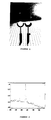
- Figure 1 is a photograph showing visibility through a large grain-size, translucent film on the left, which is compared to visibility through a small grain-size, transparent film on the right.
- Figure 2 is a graph showing the Raman spectrum for the transparent film shown in Figure 1 which shows a characteristic diamond peak at 1332 cm -1 .
- Figure 3 is a graph optical transmission through the transparent film shown in Figure 1.
- Figure 4 is an optical micrograph of a detail of the diamond film coated IC structure.
- the lightest colored patterns correspond to aluminum metallization.
- Figures 5A and 5B are cross-sectional drawings of a diamond coated bipolar junction transistor with collector (C), emitter (E), and base (B), and a diffused resistor. Solid black is aluminum, dotted gray is oxide and cross-hatched is diamond.
- the substrate can be polished with a diamond powder (preferably 0.05 to 1 ⁇ m).
- the substrate can then be subjected to CVD to produce a fine grained film which is more transparent than when the substrate is coated with the diamond particles prior to CVD.
- the diamond particles applied to the substrate before CVD have a particle width between about 0.05 and 1 micrometer. This enables the production of the adherent films using the process of the invention.
- a photoresist is admixed with the diamond particles such as SHIPLEY 1813, Shipley Marlborough, MA which is a mixture of a resin and a photoactive compound (diazo-oxide). Many such photoresist materials are well known to those skilled in the art.
- the diamond particles can also be applied to the surface suspended in an organic liquid, such as isopropanol, which is volatilized from the substrate. Spin-coating is preferred as is known in the art.
- the mole ratios of the flowing mixed gases are between about 0.90 to 0.99 for hydrogen, 0 to 0.05 for carbon dioxide and 0.01 to 0.05 for methane.
- the flow rate is preferably 200 SCCM.
- a flow rate range of 50 SCCM to 500 SCCM can be used. As can be seen, there is always a significant molar excess of hydrogen to maintain reducing conditions in the plasma.
- the films produced are generally between about 0.5 and 3.0 micrometers thick. Such films require about 5 to 40 hours to produce on the substrate.
- the substrate is preferably a silicon or glassy material, particularly a silicon wafer or borosilicate glass. Glass substrates are difficult to coat.
- a positive voltage bias can be applied to the substrate. This enables endless control of film morphology (i.e. crystal size and shape).
- the bias on the substrate is positive between about 80 and 120 DCV.
- the microwaves used to create the plasma are preferably at 2.45 GHz. Other microwave frequencies such as 915 MHz can be used.
- the power input is preferably 300 to 1500 watts.
- the preferred apparatus is described in U.S. Patent No. 5,311,103 to Asmussen et al with a graphite support for the substrate. Numerous other configurations for producing a resonant RF or microwave plasma source can be used as is well known to those skilled in the art.
- Microwave plasma-assisted chemical vapor deposition can be used to deposit continuous and adhering diamond films on borosilicate glasses that exhibit 70% optical transmission. Such films require low substrate temperatures, between 400°C and 600°C, during deposition.
- Diamond over-coatings on substrates which contain microelectronic circuitry provide a means for reduction of thermal hot-spots, or act as a superior passivation layer.
- This invention includes microwave plasma-assisted chemical vapor deposition of diamond on silicon substrates which contain microelectronic devices. Deposition temperatures are compatible with the aluminum metallization technology commonly used in integrated circuit fabrication. Both passive devices (diffused resistors) and active devices (transistors) are successfully coated.
- the substrate was CORNING 7059 glass (Dow Corning, Midland, Michigan) wafer, 5 cm (2 inches) in diameter and 1.1 mm thick.
- the substrate was seeded by 0.1 micrometer diamond powder suspended in photoresist (SHIPLEY 1813) which was spun onto the wafer.
- Film deposition was performed in a microwave plasma disk reactor with a 10 cm (4 inch) diameter bell jar at a pressure of 933 Pa (7 torr) and with gas flows of 200 sccm hydrogen, 8 sccm carbon dioxide, and 3 sccm methane. Deposition time was 40 hours, the microwave input power was 350 W, and the substrate temperature as measured with an optical pyrometer was 465°C.
- the resulting film was continuous as documented by microscopy, and was high-quality polycrystalline diamond as documented by Raman analysis.
- the average thickness was 1.24 micrometers as determined by weight gain measurements.
- the tape-test (performed using 3M Scotch Magic tape, 19 mm wide) still yielded an intact, adhering diamond film on glass.
- Example 1 diamond was deposited using a low-temperature microwave plasma-assisted CVD method of the present invention.
- the results are generally described by the inventors in Ulczynski, M. J., et al., Advances in New Diamond Science and Technology, Eds. S. Saito, et al., MYU, Tokyo, (1994). Seeding of the substrates was performed either by a spin-on method as described by Masood et al (Masood, A., et al., J. Electrochem. Soc., 138 L67-L68 (1991)), or by polishing with fine diamond powder.
- the substrate temperature during deposition was varied between 400°C and 520°C as measured by optical pyrometry. Substrates up to 10 cm in diameter have been coated with deposition rates of 1 mg per hour by this method.
- the resulting films are generally in a state of compression since the thermal expansion coefficient of the glass substrates is approximately twice that of diamond.
- Many films have shown good long-term adhesion with, for example, diamond films on both Corning 7059 and PYREX substrates that pass the tape test for adhesion one year after adhesion, and after repeated thermal cycling to 200°C.
- Other films have shown spontaneous delamination after times ranging from several minutes to several days after removal from the deposition chamber.
- the most obvious variables affecting adhesion are deposition temperature and film thickness since film stress increases as both of these parameters increase. Long term adhesion is best achieved when film thicknesses are less than 3 ⁇ m and deposition temperatures are less than 480°C.
- the optical properties of the films are highly dependent on the grain size of the poly-crystalline film. Larger grain films with average grain sizes on the order of a micrometer, are translucent, having the appearance of frosted glass. Objects are clearly visible through such films only if they are directly adjacent to the diamond film. In contrast, smaller grain films, with grain sizes on the order of a quarter-micrometer, are transparent. This difference is illustrated in Figure 1 in which the optical table features are clearly visible through the small grain film, but not the large grain film. Both films however are high quality diamond as indicated by Raman spectroscopy. A Raman spectra, taken with a 30 ⁇ m diameter, 488 nm Argon laser, for the transparent film in Figure 1 is shown in Figure 2. The polishing of the glass substrate with the diamond particles resulted in the clear, fine grained films.
- This example illustrates adhesion of diamond films on glass after temperature-cycling.
- the substrate was CORNING 7059 glass wafer, 5 cm (2 inches) in diameter and 1.1 mm thick.
- the substrate was seeded by 0.1 micrometer diamond powder suspended in photoresist (SHIPLEY 1813) which was spun onto the wafer.
- Film deposition was performed in a microwave plasma disk reactor with a 12,7 cm (5 inch) diameter bell jar at a pressure of 9 torr and with gas flows of 200 sccm hydrogen, 8 sccm carbon dioxide, and 3 sccm methane. Deposition time was 38 hours, the microwave input power was 1000 W, and the substrate temperature as measured with an optical pyrometer was 450°C.
- the resulting polycrystalline diamond film was continuous as documented by microscopy, and was high-quality diamond as documented by Raman analysis.
- the average thickness was 1.0 micrometers as determined by weight gain measurements.
- the sample was heated to a fixed temperature and then cooled to room temperature in a series of experiments. After each experiment, the tape-test was performed. The temperatures to which the sample was heated were 80°C, 125°C and 210°C. After each experiment, the sample passed the tape-test for adhesion.
- This example illustrates adhesion of diamond films on glass after temperature-cycling for a different gas composition and a different substrate size.
- the substrate was CORNING 7059 glass wafer, 7,6 cm (3 inches) in diameter and 1.1 mm thick.
- the substrate was seeded by 0.1 micrometer diamond powder suspended in photoresist which was spun onto the wafer.
- Film deposition was performed in a microwave plasma disk reactor with a 12,7 cm (5 inch) diameter bell jar at a pressure of 1200 Pa (9 torr) and with gas flows of 200 sccm hydrogen and 5 sccm methane. Deposition time was 30 hours, the microwave input power was 1000 W, and the substrate temperature as measured with an optical pyrometer was 470°C.
- the resulting polycrystalline diamond film was continuous as documented by microscopy, and was high-quality diamond as documented by Raman analysis. The average thickness was 2.0 micrometers as determined by weight gain measurements.
- the sample was heated to a fixed temperature and then cooled to room temperature in a series of experiments. After each experiment, the tape test was performed. The temperatures to which the sample was heated were 80°C, 125°C, and 210°C. After each experiment, the sample passed the tape-test for adhesion.
- This example illustrates adhesion of diamond films on glass for a different glass-type.
- the substrate was PYREX glass wafer, 5 cm (2 inches) in diameter and 2 mm thick.
- the substrate was seeded by 0.1 micrometer diamond powder suspended in photoresist SHIPLEY 1813 which was spun onto the wafer.
- Film deposition was performed in a microwave plasma disk reactor with a 5 inch diameter bell jar at a pressure of 9 torr and with gas flows of 200 sccm hydrogen, 8 sccm carbon dioxide, and 3 sccm methane. Deposition time was 60 hours, the microwave input power was 1000 W, and the substrate temperature as measured with an optical pyrometer was 470°C.
- the average polycrystalline diamond film thickness was 1.7 micrometers as determined by weight gain measurements. The sample passed the tape-test for adhesion.
- Silicon integrated circuits consist of a variety of materials including silicon, silicon dioxide, and aluminum based metal layer. These represent a wide variety of thermal expansion coefficients and whereas diamond deposition on silicon is well established, deposition on metals and oxides can be problematic. An upper limit on deposition temperature is imposed by the presence of aluminum which has a melting temperature of 660°C. Lower substrate temperatures are advantageous in that differing thermal expansion coefficients can cause considerable intrinsic stress as the substrate and film are cooled from the deposition temperature. Consequently, low-temperature diamond deposition using microwave plasma-assisted chemical vapor deposition was used.
- Silicon substrates with (100) orientation were processed to fabricate resistors and bipolar junction transistors. Boron diffusion through oxide windows were used to form diffused resistors and p-type base regions for the transistors. A subsequent phosphorus diffusion was used to form the n-type emitter regions for the transistors, and ohmic contacts to the n-type collectors. Contact cuts were made to the underlying silicon and aluminum was deposited by thermal evaporation. The aluminum layer was patterned and etched by conventional photolithography to form contact pads for device testing purposes. An oxide passivation layer was not used.
- Figure 4 shows a 100X optical micrograph view of details of the IC structure beneath the transparent diamond film. Higher magnification shows the diamond film to be continuous and polycrystalline. The lightest features in Figure 4 correspond to aluminum patterns which are 20 ⁇ m wide. The other varying patterns correspond to oxide layers of different thickness.
- Figures 5A and 5B show cross-sectional drawings through the contact cuts of a resistor and a bipolar transistor. As measured by optical pyrometry, the substrate temperature during deposition was approximately 435°C. Based on before and after weight gain measurements, the diamond film thickness is approximately 0.7 ⁇ m.
- spin-on-glass was used as the masking layer.
- the SOG was patterned by photoresist and wet etching, the photoresist was stripped, and the diamond was etched through to the aluminum test pads.
- Diamond etching was achieved in an ECR plasma discharge using a mixture of gases including oxygen/argon/SF6.
- Diamond film coated resistors and transistors were tested subsequent to this etching procedure and found to be fully functional.
- the photoresist may be patterned prior to deposition. As noted in Masood et al, such seeding is not present where the diamond film is not desired.
- Diamond over-coatings are of interest for microelectronics because of potential applications for passivation and reduction of local hot spots.
- diamond films have been deposited on silicon integrated circuit structures including transistors and resistors. The deposition temperature is sufficiently low so as to not cause damage to the underlying structures, including the aluminum metallization.
- This example illustrates achievement of a high degree of optical transparency for diamond film on glass.
- the substrate was CORNING 7059 glass wafer, 5 cm (2 inches) in diameter and 1.1 mm thick.
- the substrate was seeded by polishing with 0.1 micrometer diamond powder and then cleaned.
- Film deposition was performed in a microwave plasma disk reactor with a 12,7 cm (5 inch) diameter bell jar at a pressure of 1200 Pa (9 torr) and with gas flows of 200 sccm hydrogen, 8 sccm carbon dioxide, and 3 sccm methane. Deposition time was 30 hours, the microwave input power was 1000 W, and the substrate temperature as measured with an optical pyrometer was 470°C.
- the resulting polycrystalline diamond film was continuous as documented by microscopy, and was high-quality diamond as documented by Raman analysis. The average thickness was 0.6 micrometers as determined by weight gain measurements.
- the seeding method produces a high seeding density such that the average grain size as determined by scanning electron microscopy is approximately 0.3 micrometers, resulting in an optically smooth film.
- Optical transmission was measured with a 0.5 mm diameter HeNe laser beam incident on the back of the glass substrate and a 1 cm diameter detector directly adjacent to the diamond film. The percent transmission was 70%. This is appreciably larger than that measured with larger grain size films (greater than one micrometer grain size) for which the percent transmission is 30%.
- calculations based on refractive indices for a perfect planar, non-absorbing diamond film on CORNING 7059 glass yield a percent transmission of 75% based on reflection at the air/glass; glass/diamond; diamond/air interfaces.
- This example illustrates the effect of substrate bias on diamond film morphology.
- the substrate was a silicon wafer, 5 cm (2 inches) in diameter and 0.3 mm thick.
- the substrate was seeded by 0.1 micrometer diamond powder suspended in photoresist which was spun onto the wafer.
- Film deposition was performed in a microwave plasma disk reactor with a 12,7 cm (5 inch) diameter bell jar at a pressure of 2000 Pa (15 torr) and with gas flows of 200 sccm hydrogen, 8 sccm carbon dioxide and 3 sccm methane. Deposition time was 40 hours, the microwave input power was 1000 W, and the substrate temperature as measured with an optical pyrometer was 510°C.
- the substrate was biased with 100 volts positive dc voltage with a resulting bias current of 8 mA by being placed on a graphite susceptor.
- the average thickness was 2.2 micrometers as determined by weight gain measurements.
- the resulting weight gain is comparable to that achieved with no-bias growth conditions, however scanning electron microscopy shows that the film resulting from deposition on a biased substrate exhibits diamond grains which are more clearly faceted than for films produced on non-biased substrates.
- the process of the present invention provides clear and adherent films on silicon containing materials. This result is achieved because of the unique set of processing conditions.
Landscapes
- Chemical & Material Sciences (AREA)
- Engineering & Computer Science (AREA)
- Mechanical Engineering (AREA)
- General Chemical & Material Sciences (AREA)
- Chemical Kinetics & Catalysis (AREA)
- Materials Engineering (AREA)
- Metallurgy (AREA)
- Organic Chemistry (AREA)
- Inorganic Chemistry (AREA)
- Combustion & Propulsion (AREA)
- Plasma & Fusion (AREA)
- Physics & Mathematics (AREA)
- Crystals, And After-Treatments Of Crystals (AREA)
- Chemical Vapour Deposition (AREA)
Claims (10)
- Verfahren zum Abscheiden eines haftenden dünnen Diamantfilms auf einem Substrat durch eine chemische Dampfabscheidung aus einem Plasma, wobei das Verfahren die folgenden Schritte umfaßt:(a) Das Positionieren des Substrates, welches mit Diamantpartikeln poliert oder einheitlich mit Diamantpartikeln einer Breite von ungefähr 0,05 bis 1 µm beschichtet wurde, neben das Plasma zur Abscheidung des dünnen Diamantfilmes; und(b) Das Erzeugen des Plasmas bei einer Temperatur des Substrates von weniger als 600°C, wobei das Plasma eine Mischung von Gasen enthält, die im wesentlichen aus Wasserstoff, optional aus Kohlenstoffdioxid, und aus Methan bei einem Druck zwischen 133 und 2000 Pa (1 bis 15 Torr) besteht, um den dünnen Diamantfilm auf dem Substrat abzuscheiden, wobei der dünne Diamantfilm an dem Substrat haftet.
- Verfahren nach Anspruch 1, gekennzeichnet durch das Erzeugen eines Plasmas bei einer Temperatur des Substrates von 350-500°C, wobei das Plasma im wesentlichen aus Wasserstoff, Kohlenstoffdioxid und Methan besteht.
- Verfahren nach Anspruch 2, dadurch gekennzeichnet, daß die Molverhältnisse für Wasserstoff 0,90 bis 0,99, für Kohlendioxid 0,001 bis 0,05 und für Methan 0,01 bis 0,05 sind.
- Verfahren nach Anspruch 3, dadurch gekennzeichnet, daß zur Erzeugung des Plasmas eine Mikrowelle mit einer Frequenz von 2,45 GHz oder 915 MHz ausgewählt wird.
- Verfahren nach einem der Ansprüche 1 oder 2, dadurch gekennzeichnet, daß eine positive elektrische Vorspannung an das Substrat angelegt wird.
- Verfahren nach einem der Ansprüche 1 oder 2, dadurch gekennzeichnet, daß das Substrat aus Glas besteht.
- Verfahren nach Anspruch 6, dadurch gekennzeichnet, daß das Glas ein Glas aus Borsilicat ist.
- Verfahren nach Anspruch 2, dadurch gekennzeichnet, daß die Partikel aus Diamant in einer Zusammensetzung eines Photolacks auf das Substrat beschichtet werden.
- Verfahren nach Anspruch 2, dadurch gekennzeichnet, daß die Partikel aus Diamand zum Polieren des Substrates verwendet werden.
- Verfahren nach einem der Ansprüche 1 oder 2, dadurch gekennzeichnet, daß das Substrat ein Siliciumwafer mit elektrischen Schaltkreisen ist, die durch den dünnen Diamantfilm abgedeckt werden.
Priority Applications (4)
| Application Number | Priority Date | Filing Date | Title |
|---|---|---|---|
| CA002182245A CA2182245C (en) | 1996-07-29 | 1996-07-29 | Process for depositing adherent diamond thin films |
| EP96112277A EP0822268B1 (de) | 1996-07-29 | 1996-07-30 | Verfahren zur Erzeugung einer haftenden Diamantbeschichtung |
| DE1996607955 DE69607955T2 (de) | 1996-07-30 | 1996-07-30 | Verfahren zur Erzeugung einer haftenden Diamantbeschichtung |
| JP8212635A JP2875984B2 (ja) | 1996-07-29 | 1996-08-12 | 付着力のあるダイヤモンド薄膜の蒸着方法 |
Applications Claiming Priority (3)
| Application Number | Priority Date | Filing Date | Title |
|---|---|---|---|
| CA002182245A CA2182245C (en) | 1996-07-29 | 1996-07-29 | Process for depositing adherent diamond thin films |
| EP96112277A EP0822268B1 (de) | 1996-07-29 | 1996-07-30 | Verfahren zur Erzeugung einer haftenden Diamantbeschichtung |
| JP8212635A JP2875984B2 (ja) | 1996-07-29 | 1996-08-12 | 付着力のあるダイヤモンド薄膜の蒸着方法 |
Publications (2)
| Publication Number | Publication Date |
|---|---|
| EP0822268A1 EP0822268A1 (de) | 1998-02-04 |
| EP0822268B1 true EP0822268B1 (de) | 2000-04-26 |
Family
ID=27170177
Family Applications (1)
| Application Number | Title | Priority Date | Filing Date |
|---|---|---|---|
| EP96112277A Expired - Lifetime EP0822268B1 (de) | 1996-07-29 | 1996-07-30 | Verfahren zur Erzeugung einer haftenden Diamantbeschichtung |
Country Status (3)
| Country | Link |
|---|---|
| EP (1) | EP0822268B1 (de) |
| JP (1) | JP2875984B2 (de) |
| CA (1) | CA2182245C (de) |
Families Citing this family (6)
| Publication number | Priority date | Publication date | Assignee | Title |
|---|---|---|---|---|
| EP1748091A4 (de) * | 2004-04-19 | 2012-11-28 | Nat Inst Of Advanced Ind Scien | Kohlenstofffilm |
| JP2009091234A (ja) * | 2007-09-18 | 2009-04-30 | Tokyo Univ Of Science | 導電性ダイヤモンド膜が形成された基板及び導電性ダイヤモンド膜が形成された基板の製造方法 |
| GB2476478A (en) * | 2009-12-22 | 2011-06-29 | Element Six Ltd | Chemical vapour deposition diamond synthesis |
| JP5652927B2 (ja) | 2011-05-10 | 2015-01-14 | 独立行政法人産業技術総合研究所 | 炭素膜積層体、並びにその積層体の製造方法及びそれを用いた潤滑材 |
| US12037703B2 (en) * | 2015-02-06 | 2024-07-16 | Ecotricity Group Limited | Method of producing a synthetic diamond |
| CN112361973B (zh) * | 2020-11-18 | 2022-07-29 | 华侨大学 | 一种金刚石薄膜厚度及光学常数检测方法 |
Family Cites Families (1)
| Publication number | Priority date | Publication date | Assignee | Title |
|---|---|---|---|---|
| JPH04214094A (ja) * | 1990-04-26 | 1992-08-05 | Hitachi Ltd | 合成ダイヤモンド薄膜の製法、該薄膜及びそれを用いた装置 |
-
1996
- 1996-07-29 CA CA002182245A patent/CA2182245C/en not_active Expired - Fee Related
- 1996-07-30 EP EP96112277A patent/EP0822268B1/de not_active Expired - Lifetime
- 1996-08-12 JP JP8212635A patent/JP2875984B2/ja not_active Expired - Fee Related
Also Published As
| Publication number | Publication date |
|---|---|
| JPH1095694A (ja) | 1998-04-14 |
| JP2875984B2 (ja) | 1999-03-31 |
| EP0822268A1 (de) | 1998-02-04 |
| CA2182245C (en) | 2000-09-26 |
| CA2182245A1 (en) | 1998-01-30 |
Similar Documents
| Publication | Publication Date | Title |
|---|---|---|
| US5897924A (en) | Process for depositing adherent diamond thin films | |
| CA1337855C (en) | Processes for the preparation of polycrystalline diamond films | |
| Suzuki et al. | Epitaxial growth of β-SiC single crystals by successive two-step CVD | |
| Chakrabarti et al. | Nano-diamond films produced from CVD of camphor | |
| EP0543392A2 (de) | Diamant-Halbleiteranordnung und Verfahren zu ihrer Herstellung | |
| JP2002265296A (ja) | ダイヤモンド薄膜及びその製造方法 | |
| EP0822268B1 (de) | Verfahren zur Erzeugung einer haftenden Diamantbeschichtung | |
| US5686152A (en) | Metal initiated nucleation of diamond | |
| Dusane et al. | Hydrogenated microcrystalline silicon films produced at low temperature by the hot wire deposition method | |
| US5204210A (en) | Method for the direct patterning of diamond films | |
| Yang et al. | Ultrahigh nucleation density for growth of smooth diamond films | |
| US5221501A (en) | Method of producing a smooth plate of diamond | |
| US5304461A (en) | Process for the selective deposition of thin diamond film by gas phase synthesis | |
| Chayahara et al. | Properties of BN thin films deposited by plasma CVD | |
| GB2260341A (en) | Selective imagewise deposition of thin diamond film on a diamond film | |
| Kundu et al. | Nanocrystalline diamond films deposited by high pressure sputtering of vitreous carbon | |
| JP3252926B2 (ja) | ダイヤモンド被覆体およびその製造方法 | |
| JP2025540656A (ja) | 多層ダイヤモンドディスプレイシステムおよびその方法 | |
| Knox et al. | Amorphous and polycrystalline silicon films deposited by electron cyclotron resonance reactive plasma deposition | |
| Pinarbasi et al. | Hydrogenated amorphous silicon films deposited by DC planar magnetron reactive sputtering | |
| DE69607955T2 (de) | Verfahren zur Erzeugung einer haftenden Diamantbeschichtung | |
| Williams et al. | Plasma enhanced chemical vapor deposition of epitaxial mercury telluride | |
| Tetsuro Maki et al. | Selective homoepitaxy of diamond thin films and investigation of their cathodoluminescence | |
| KR970000381B1 (ko) | 실리카 유리에 다이아몬드 박막을 코팅하는 방법 | |
| Huang et al. | Structural and electrical characterization of AIN thin films obtained by nitridation of Al/Si substrate |
Legal Events
| Date | Code | Title | Description |
|---|---|---|---|
| PUAI | Public reference made under article 153(3) epc to a published international application that has entered the european phase |
Free format text: ORIGINAL CODE: 0009012 |
|
| 17P | Request for examination filed |
Effective date: 19960730 |
|
| AK | Designated contracting states |
Kind code of ref document: A1 Designated state(s): DE FR GB |
|
| AKX | Designation fees paid |
Free format text: DE FR GB |
|
| RBV | Designated contracting states (corrected) |
Designated state(s): DE FR GB |
|
| 17Q | First examination report despatched |
Effective date: 19990201 |
|
| GRAG | Despatch of communication of intention to grant |
Free format text: ORIGINAL CODE: EPIDOS AGRA |
|
| GRAG | Despatch of communication of intention to grant |
Free format text: ORIGINAL CODE: EPIDOS AGRA |
|
| GRAH | Despatch of communication of intention to grant a patent |
Free format text: ORIGINAL CODE: EPIDOS IGRA |
|
| GRAH | Despatch of communication of intention to grant a patent |
Free format text: ORIGINAL CODE: EPIDOS IGRA |
|
| GRAA | (expected) grant |
Free format text: ORIGINAL CODE: 0009210 |
|
| AK | Designated contracting states |
Kind code of ref document: B1 Designated state(s): DE FR GB |
|
| REF | Corresponds to: |
Ref document number: 69607955 Country of ref document: DE Date of ref document: 20000531 |
|
| ET | Fr: translation filed | ||
| PLBE | No opposition filed within time limit |
Free format text: ORIGINAL CODE: 0009261 |
|
| STAA | Information on the status of an ep patent application or granted ep patent |
Free format text: STATUS: NO OPPOSITION FILED WITHIN TIME LIMIT |
|
| 26N | No opposition filed | ||
| REG | Reference to a national code |
Ref country code: GB Ref legal event code: IF02 |
|
| PGFP | Annual fee paid to national office [announced via postgrant information from national office to epo] |
Ref country code: FR Payment date: 20090710 Year of fee payment: 14 |
|
| PGFP | Annual fee paid to national office [announced via postgrant information from national office to epo] |
Ref country code: GB Payment date: 20090729 Year of fee payment: 14 |
|
| PGFP | Annual fee paid to national office [announced via postgrant information from national office to epo] |
Ref country code: DE Payment date: 20100728 Year of fee payment: 15 |
|
| GBPC | Gb: european patent ceased through non-payment of renewal fee |
Effective date: 20100730 |
|
| REG | Reference to a national code |
Ref country code: FR Ref legal event code: ST Effective date: 20110331 |
|
| PG25 | Lapsed in a contracting state [announced via postgrant information from national office to epo] |
Ref country code: FR Free format text: LAPSE BECAUSE OF NON-PAYMENT OF DUE FEES Effective date: 20100802 |
|
| PG25 | Lapsed in a contracting state [announced via postgrant information from national office to epo] |
Ref country code: GB Free format text: LAPSE BECAUSE OF NON-PAYMENT OF DUE FEES Effective date: 20100730 |
|
| PG25 | Lapsed in a contracting state [announced via postgrant information from national office to epo] |
Ref country code: DE Free format text: LAPSE BECAUSE OF NON-PAYMENT OF DUE FEES Effective date: 20120201 |
|
| REG | Reference to a national code |
Ref country code: DE Ref legal event code: R119 Ref document number: 69607955 Country of ref document: DE Effective date: 20120201 |