EP0822541A2 - Senseur à magnetoresistance géante non-magnétique et autopolarisé - Google Patents
Senseur à magnetoresistance géante non-magnétique et autopolarisé Download PDFInfo
- Publication number
- EP0822541A2 EP0822541A2 EP97113010A EP97113010A EP0822541A2 EP 0822541 A2 EP0822541 A2 EP 0822541A2 EP 97113010 A EP97113010 A EP 97113010A EP 97113010 A EP97113010 A EP 97113010A EP 0822541 A2 EP0822541 A2 EP 0822541A2
- Authority
- EP
- European Patent Office
- Prior art keywords
- layer
- magnetoresistive
- inhomogeneous
- sensor
- forming
- Prior art date
- Legal status (The legal status is an assumption and is not a legal conclusion. Google has not performed a legal analysis and makes no representation as to the accuracy of the status listed.)
- Withdrawn
Links
- 230000005291 magnetic effect Effects 0.000 title claims abstract description 30
- 239000000463 material Substances 0.000 claims abstract description 30
- 229910000661 Mercury cadmium telluride Inorganic materials 0.000 claims abstract description 23
- MCMSPRNYOJJPIZ-UHFFFAOYSA-N cadmium;mercury;tellurium Chemical compound [Cd]=[Te]=[Hg] MCMSPRNYOJJPIZ-UHFFFAOYSA-N 0.000 claims abstract description 23
- 239000000758 substrate Substances 0.000 claims abstract description 18
- 238000000034 method Methods 0.000 claims description 9
- 230000000694 effects Effects 0.000 claims description 8
- 238000003860 storage Methods 0.000 claims description 5
- 239000004065 semiconductor Substances 0.000 claims description 4
- MARUHZGHZWCEQU-UHFFFAOYSA-N 5-phenyl-2h-tetrazole Chemical compound C1=CC=CC=C1C1=NNN=N1 MARUHZGHZWCEQU-UHFFFAOYSA-N 0.000 claims description 2
- 230000005381 magnetic domain Effects 0.000 claims 3
- 239000002019 doping agent Substances 0.000 claims 1
- 229910004613 CdTe Inorganic materials 0.000 abstract description 3
- XUIMIQQOPSSXEZ-UHFFFAOYSA-N Silicon Chemical compound [Si] XUIMIQQOPSSXEZ-UHFFFAOYSA-N 0.000 abstract description 3
- 229910052710 silicon Inorganic materials 0.000 abstract description 3
- 239000010703 silicon Substances 0.000 abstract description 3
- 239000010409 thin film Substances 0.000 abstract description 3
- 239000000203 mixture Substances 0.000 description 6
- 230000001419 dependent effect Effects 0.000 description 5
- 239000010408 film Substances 0.000 description 5
- 238000005259 measurement Methods 0.000 description 5
- 229910045601 alloy Inorganic materials 0.000 description 4
- 239000000956 alloy Substances 0.000 description 4
- 230000007423 decrease Effects 0.000 description 4
- 229910052793 cadmium Inorganic materials 0.000 description 3
- 230000001747 exhibiting effect Effects 0.000 description 3
- 229910052753 mercury Inorganic materials 0.000 description 3
- PXHVJJICTQNCMI-UHFFFAOYSA-N Nickel Chemical compound [Ni] PXHVJJICTQNCMI-UHFFFAOYSA-N 0.000 description 2
- 230000008859 change Effects 0.000 description 2
- 238000001816 cooling Methods 0.000 description 2
- 230000003247 decreasing effect Effects 0.000 description 2
- 238000009826 distribution Methods 0.000 description 2
- 230000005294 ferromagnetic effect Effects 0.000 description 2
- 238000004519 manufacturing process Methods 0.000 description 2
- 238000012986 modification Methods 0.000 description 2
- 230000004048 modification Effects 0.000 description 2
- 229910000889 permalloy Inorganic materials 0.000 description 2
- 230000004044 response Effects 0.000 description 2
- JBRZTFJDHDCESZ-UHFFFAOYSA-N AsGa Chemical compound [As]#[Ga] JBRZTFJDHDCESZ-UHFFFAOYSA-N 0.000 description 1
- 229910001020 Au alloy Inorganic materials 0.000 description 1
- 229910001218 Gallium arsenide Inorganic materials 0.000 description 1
- 230000005357 Hall field Effects 0.000 description 1
- 229910001030 Iron–nickel alloy Inorganic materials 0.000 description 1
- 229910003266 NiCo Inorganic materials 0.000 description 1
- VYRNMWDESIRGOS-UHFFFAOYSA-N [Mo].[Au] Chemical compound [Mo].[Au] VYRNMWDESIRGOS-UHFFFAOYSA-N 0.000 description 1
- 230000005540 biological transmission Effects 0.000 description 1
- 239000000969 carrier Substances 0.000 description 1
- 150000001875 compounds Chemical class 0.000 description 1
- 239000002772 conduction electron Substances 0.000 description 1
- 239000004020 conductor Substances 0.000 description 1
- 238000010276 construction Methods 0.000 description 1
- 238000013461 design Methods 0.000 description 1
- 239000010432 diamond Substances 0.000 description 1
- 229920006333 epoxy cement Polymers 0.000 description 1
- 238000005530 etching Methods 0.000 description 1
- 238000002474 experimental method Methods 0.000 description 1
- PCHJSUWPFVWCPO-UHFFFAOYSA-N gold Chemical compound [Au] PCHJSUWPFVWCPO-UHFFFAOYSA-N 0.000 description 1
- 229910052737 gold Inorganic materials 0.000 description 1
- 239000010931 gold Substances 0.000 description 1
- 239000003353 gold alloy Substances 0.000 description 1
- 239000012535 impurity Substances 0.000 description 1
- 239000000696 magnetic material Substances 0.000 description 1
- 230000005415 magnetization Effects 0.000 description 1
- YVUZUKYBUMROPQ-UHFFFAOYSA-N mercury zinc Chemical compound [Zn].[Hg] YVUZUKYBUMROPQ-UHFFFAOYSA-N 0.000 description 1
- 238000004377 microelectronic Methods 0.000 description 1
- 238000001451 molecular beam epitaxy Methods 0.000 description 1
- 229910021421 monocrystalline silicon Inorganic materials 0.000 description 1
- 229910052759 nickel Inorganic materials 0.000 description 1
- 238000000059 patterning Methods 0.000 description 1
- 238000000206 photolithography Methods 0.000 description 1
- 238000002360 preparation method Methods 0.000 description 1
- 230000008569 process Effects 0.000 description 1
- 239000007787 solid Substances 0.000 description 1
- 230000007704 transition Effects 0.000 description 1
- 230000000007 visual effect Effects 0.000 description 1
Images




Classifications
-
- G—PHYSICS
- G11—INFORMATION STORAGE
- G11B—INFORMATION STORAGE BASED ON RELATIVE MOVEMENT BETWEEN RECORD CARRIER AND TRANSDUCER
- G11B5/00—Recording by magnetisation or demagnetisation of a record carrier; Reproducing by magnetic means; Record carriers therefor
- G11B5/127—Structure or manufacture of heads, e.g. inductive
- G11B5/33—Structure or manufacture of flux-sensitive heads, i.e. for reproduction only; Combination of such heads with means for recording or erasing only
- G11B5/39—Structure or manufacture of flux-sensitive heads, i.e. for reproduction only; Combination of such heads with means for recording or erasing only using magneto-resistive devices or effects
-
- B—PERFORMING OPERATIONS; TRANSPORTING
- B82—NANOTECHNOLOGY
- B82Y—SPECIFIC USES OR APPLICATIONS OF NANOSTRUCTURES; MEASUREMENT OR ANALYSIS OF NANOSTRUCTURES; MANUFACTURE OR TREATMENT OF NANOSTRUCTURES
- B82Y25/00—Nanomagnetism, e.g. magnetoimpedance, anisotropic magnetoresistance, giant magnetoresistance or tunneling magnetoresistance
-
- G—PHYSICS
- G01—MEASURING; TESTING
- G01R—MEASURING ELECTRIC VARIABLES; MEASURING MAGNETIC VARIABLES
- G01R33/00—Arrangements or instruments for measuring magnetic variables
- G01R33/02—Measuring direction or magnitude of magnetic fields or magnetic flux
- G01R33/06—Measuring direction or magnitude of magnetic fields or magnetic flux using galvano-magnetic devices
- G01R33/09—Magnetoresistive devices
- G01R33/093—Magnetoresistive devices using multilayer structures, e.g. giant magnetoresistance sensors
-
- G—PHYSICS
- G11—INFORMATION STORAGE
- G11B—INFORMATION STORAGE BASED ON RELATIVE MOVEMENT BETWEEN RECORD CARRIER AND TRANSDUCER
- G11B5/00—Recording by magnetisation or demagnetisation of a record carrier; Reproducing by magnetic means; Record carriers therefor
- G11B5/127—Structure or manufacture of heads, e.g. inductive
- G11B5/33—Structure or manufacture of flux-sensitive heads, i.e. for reproduction only; Combination of such heads with means for recording or erasing only
-
- G—PHYSICS
- G11—INFORMATION STORAGE
- G11B—INFORMATION STORAGE BASED ON RELATIVE MOVEMENT BETWEEN RECORD CARRIER AND TRANSDUCER
- G11B5/00—Recording by magnetisation or demagnetisation of a record carrier; Reproducing by magnetic means; Record carriers therefor
- G11B5/127—Structure or manufacture of heads, e.g. inductive
- G11B5/33—Structure or manufacture of flux-sensitive heads, i.e. for reproduction only; Combination of such heads with means for recording or erasing only
- G11B5/37—Structure or manufacture of flux-sensitive heads, i.e. for reproduction only; Combination of such heads with means for recording or erasing only using galvano-magnetic devices, e.g. Hall-effect devices using Hall or Hall-related effect, e.g. planar-Hall effect or pseudo-Hall effect
- G11B5/376—Structure or manufacture of flux-sensitive heads, i.e. for reproduction only; Combination of such heads with means for recording or erasing only using galvano-magnetic devices, e.g. Hall-effect devices using Hall or Hall-related effect, e.g. planar-Hall effect or pseudo-Hall effect in semi-conductors
-
- G—PHYSICS
- G11—INFORMATION STORAGE
- G11B—INFORMATION STORAGE BASED ON RELATIVE MOVEMENT BETWEEN RECORD CARRIER AND TRANSDUCER
- G11B5/00—Recording by magnetisation or demagnetisation of a record carrier; Reproducing by magnetic means; Record carriers therefor
- G11B5/127—Structure or manufacture of heads, e.g. inductive
- G11B5/33—Structure or manufacture of flux-sensitive heads, i.e. for reproduction only; Combination of such heads with means for recording or erasing only
- G11B5/39—Structure or manufacture of flux-sensitive heads, i.e. for reproduction only; Combination of such heads with means for recording or erasing only using magneto-resistive devices or effects
- G11B5/3903—Structure or manufacture of flux-sensitive heads, i.e. for reproduction only; Combination of such heads with means for recording or erasing only using magneto-resistive devices or effects using magnetic thin film layers or their effects, the films being part of integrated structures
- G11B5/3993—Structure or manufacture of flux-sensitive heads, i.e. for reproduction only; Combination of such heads with means for recording or erasing only using magneto-resistive devices or effects using magnetic thin film layers or their effects, the films being part of integrated structures in semi-conductors
-
- H—ELECTRICITY
- H10—SEMICONDUCTOR DEVICES; ELECTRIC SOLID-STATE DEVICES NOT OTHERWISE PROVIDED FOR
- H10N—ELECTRIC SOLID-STATE DEVICES NOT OTHERWISE PROVIDED FOR
- H10N50/00—Galvanomagnetic devices
- H10N50/10—Magnetoresistive devices
-
- H—ELECTRICITY
- H10—SEMICONDUCTOR DEVICES; ELECTRIC SOLID-STATE DEVICES NOT OTHERWISE PROVIDED FOR
- H10N—ELECTRIC SOLID-STATE DEVICES NOT OTHERWISE PROVIDED FOR
- H10N52/00—Hall-effect devices
- H10N52/101—Semiconductor Hall-effect devices
Definitions
- the present invention relates generally to sensors for reading information signals recorded in a magnetic medium and, more particularly, to a self-biasing, non-magnetic giant magnetoresistance (GMR) sensor.
- GMR giant magnetoresistance
- sensors exhibiting magnetoresistive characteristics are known and implemented in systems for the reading of information signals recorded in a magnetic medium such as tapes, drums and diskettes.
- These sensors typically comprise a block made of a ferromagnetic alloy exhibiting high magnetoresistance.
- a recording medium passing in close proximity to such a sensor causes variations in the magnetic field at the position of the read head, and hence variations of the electrical resistance of the magnetoresistive sensor.
- the alloys most frequently used are nickel-based ferromagnetic alloys such as NiCo or NiFe (Permalloy) which have high magnetoresistance but which, at ambient temperatures, give a relative variation in resistance of only a few percent at the relevant (average) magnetic fields ( ⁇ 50G) accessible to those particular sensors.
- magnetoresistive sensors have been described exhibiting a form of magnetoresistance generally known as "spin-valve” (SV) magnetoresistance, in which the change in resistance of the sensor is attributed to the spin-dependent transmission of conduction electrons between the magnetic layers of the sensor and the accompanying spin-dependent scattering at the layer interfaces.
- SV spin-valve
- the magnetoresistance is observed to vary as the cosine of the angle between the magnetizations of the layers and is dependent of the direction of current flow through the sensor.
- sensors do exhibit a magnetoresistance that, for selected combinations of materials, is greater in magnitude than that exhibited by the alloy magnetoresistors (AMR), they too suffer from having a relatively small variation in magnetoresistance at ambient temperatures.
- magnetoresistive sensors for reading/writing information signals stored on a magnetic medium have been described in copending applications Serial No. 08/396,819 filed on March 2, 1995 and Serial No. 08/435,254 filed on May 5, 1995, each assigned to the same assignee as the instant application and incorporated herein by reference.
- Magnetoresistive sensors are normally fabricated with a thin overlayer of hard magnetic material to provide a bias field required for optimum performance.
- MCT Mercury Cadmium Telluride
- the present invention is a self-biasing, non-magnetic giant magnetoresistive sensor constructed from a thin film of non-homogeneous magnetoresistive material, i.e., Mercury Cadmium Telluride.
- the thin film may be advantageously grown using a variety of techniques.
- the present invention is directed to such a self-biasing, non-magnetic magnetoresistive sensor having a silicon substrate, a buffer layer of undoped CdTe or other lattice-matched compound overlying the substrate, a non-homogeneous magnetoresistive layer, i.e., Hg 1-x Cd x Te, and electrodes attached to the non-homogeneous layer.
- a self-biasing, non-magnetic magnetoresistive sensor having a silicon substrate, a buffer layer of undoped CdTe or other lattice-matched compound overlying the substrate, a non-homogeneous magnetoresistive layer, i.e., Hg 1-x Cd x Te, and electrodes attached to the non-homogeneous layer.
- the present invention is directed to a read/write head containing a self-biasing, non-magnetic magnetoresistive sensor having a Corbino structure, particularly well suited for reading information signals stored in a magnetic medium with high storage density.
- Figs. 1(a) and 1(b) show a Corbino disc-type magnetoresistive sensor of the present invention.
- a non-homogeneous magnetoresistive layer 110 was deposited upon a semiconductor substrate 100.
- the non-homogeneous layer may be made of Mercury Cadmium Telluride, Hg 1-x Cd x Te, where x varies throughout the material thereby imparting the non-homogeneous characteristic.
- Conductive electrodes 120, 130 were applied to the magnetoresistive layer by standard photolithographic techniques.
- Leads, 135, 137 may then be attached to the electrodes by any of a variety of conductive means, e.g., conductive epoxy cement or gold/bonding wire.
- buffer layer 105 may be applied between the substrate and the non-homogeneous magnetoresistive layer.
- the buffer layer may be made of any material compatible with the substrate and the magnetoresistive layer, e.g., Cadmium Telluride.
- Hg 1-x Cd x Te films were grown on single crystal Si substrates by conventional molecular-beam epitaxy (MBE) techniques using methods well known in the art.
- MBE molecular-beam epitaxy
- a ⁇ 4 ⁇ m buffer layer of undoped CdTe separated the substrate and the 4.6 ⁇ m thick Hg 1-x Cd x Te layer in the sensor depicted by Fig. 1(b).
- Figs 1(c) and 1(d) show plan views of magnetoresistive sensors (Hall bar and Corbino disc) which have been constructed according to the present invention.
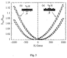
- Fig. 3 is shown the room temperature low-field (H ⁇ 0.1T) GMR measured in the Corbino disc geometry.
- the GMR defined hereafter as R Cor (H)/R Cor (0) where R Cor (H ), is quadratic in field (see below).
- R Cor (H ) is quadratic in field (see below).
- H O ⁇ -145 Gauss of the minimum in the GMR
- H O is of the same magnitude but opposite sign. This offset is much larger than the remnant magnetic field in the superconducting magnet ( ⁇ 20G).
- the zero-field offset, H 0 constitutes a self-biasing of the Corbino device. Before identifying the origin of this self biasing effect it will be useful to describe additional measurements of the magnetotransport properties.
- the low-field GMR was measured as a function of temperature, and fitted at each temperature to a parabolic dependence on the magnetic field.
- the position of the minimum, H O is plotted in Fig. 4 as a function of temperature.
- the offset is largest at high temperature, and decreases to a value of order the remanent field at low temperature.
- the temperature dependence of H O is similar, but the magnitude at room temperature varies between 100 and 350G.
- R j (T) C j ⁇ (T) where ⁇ ( T ) is the temperature-dependent resistivity of the MCT.
- r b (r a ) is the outer (inner) radius of the Corbino disc and t is the MCT film thickness, while l (A) is the length (cross-sectional area) of the Hall bar.
- V Cor IR Cor ( 1+ ⁇ H 2 )
- I the radial current in the CD
- H the applied field perpendicular to the CD
- ⁇ ( e ⁇ /m * c ) 2
- R Cor C Cor ⁇ 0 Cor 1+ ⁇ ⁇ 0 Cor
- a Hall A Cor / 1- ⁇ ⁇ 0 Cor C ' Hall C Cor .
- ⁇ ⁇ 0 Cor - ⁇ 0 Hall ,- ⁇ ⁇ ⁇ 0 Cor , and ⁇ 0 Cor , A Cor , are the resistivity and area of the homogeneous Corbino region with the corresponding values for the inhomogeneous (Hall) regions designated by the subscript Hall.
- V T (H) IR Cor (1+ ⁇ H 2 )+ R Hall IHC′ Hall ⁇ ⁇ 0 Cor .
- a value of 0.26%/K is found which is approximately equal to the corresponding value for currently available commercial magnetic MR sensors (0.238%/K) but larger than that of spin valves (0.169%/K). It may be possible to increase the thermal stability of MCT by increasing the acceptor concentration to raise die temperature of the saturation region to room temperature.
- a further example of the present invention comprises
- the active element is preferably formed by a Corbino structure that includes a layer of a magnetoresistive material that exhibits a strong magnetoresistive effect.
- the active element further includes a first inner electrode that is surrounded by the magnetoresistive material and a second outer electrode that surrounds the inner electrode in a manner characteristic of a Corbino structure.
- the outer electrode which is shown rectangular in shape, has a long dimension of about 5 ⁇ m to match approximately the width of a track of the magnetic medium and a narrow dimension of about 5000 to 1,000 Angstroms.
- Typical dimensions of the inner electrode are a length of about 1 ⁇ m and a width of about 200 to 400 Angstroms.
- the active element position on the reading head is prepared as follows. First, there is prepared a suitable substrate 20, as shown in Fig. 2A, advantageously of a semiconductor such as silicon, gallium arsenide or other material upon which there can be grown subsequent layers. A top surface 20A of the substrate may be doped or coated to be sufficiently conductive to serve well as one terminal of the sensor. There is then deposited over the substrate surface, a first layer 21, which may advantageously be the same semiconductive material as the substrate, though essentially undoped. Advantageously, and as shown in Fig. 2B, this layer is deposited to be essentially monocrystalline. As shown in Fig. 2B, layer 21 is patterned to be narrower and shorter than the substrate. The patterning may be performed through the use of techniques well-known in the microelectronics industry such as photolithography and etching.
- a suitable substrate 20A advantageously of a semiconductor such as silicon, gallium arsenide or other material upon which there can be grown subsequent layers.
- a top surface 20A of the substrate may
- This second layer 22 is a material having desirable magnetoresistive properties, such as zero-gap mercury cadmium telluride or mercury zinc telluride.
- this layer may be grown as a highly crystalline layer.
- a third layer 23 of a conductive material such as a molybdenum-gold alloy that will make good ohmic connection to the second layer.
- This third layer is deposited and patterned to be narrower than the second layer 22.
- a fourth layer 24 of magnetoresistive material is deposited to bridge the metallic layer 23 and form a continuous loop of magnetoresistive material around the conductive third layer 23.
- This fourth layer while made from the same general magnetoresistive material as the second layer 22, has sufficient compositional variation from the second layer material such that a continuous, yet inhomogeneous loop of magnetoresistive material surrounds the conductive layer.
- the second layer 22 were made from MCT having the general formula Hg 1-x Cd x Te where x ⁇ .1
- the fourth layer may be made from MCT having the general formula Hg 1-x Cd x Te where x varies throughout the fourth layer or where x second layer ⁇ x fourth layer .
- This fourth layer is patterned, as shown, so that the metallic layer is centered within the loop but there is left exposed an end portion 23A of the conductive layer 23 to which a terminal connection may subsequently be made.
- a fifth layer 25 advantageously of the same material as the first layer 21, and is patterned to form a bridge over the fourth layer 24 and a continuous loop that surrounds the fourth layer 24.
- a fifth layer 25 advantageously of the same material as the first layer 21, and is patterned to form a bridge over the fourth layer 24 and a continuous loop that surrounds the fourth layer 24.
- the basic elements of the magnetoresistive sensor are now essentially in place. There remains the need to diffuse an impurity into the exposed front face of the stack to dope the exposed front edge of the loop of undoped semiconductor formed of the first and fifth layers (21,25) to a conductive state so that the doped loop can serve as the conductive outer electrode of the Corbino structure.
Landscapes
- Engineering & Computer Science (AREA)
- Manufacturing & Machinery (AREA)
- Physics & Mathematics (AREA)
- Chemical & Material Sciences (AREA)
- Nanotechnology (AREA)
- Condensed Matter Physics & Semiconductors (AREA)
- General Physics & Mathematics (AREA)
- Crystallography & Structural Chemistry (AREA)
- Hall/Mr Elements (AREA)
- Magnetic Heads (AREA)
Applications Claiming Priority (2)
| Application Number | Priority Date | Filing Date | Title |
|---|---|---|---|
| US688583 | 1996-07-30 | ||
| US08/688,583 US5696655A (en) | 1996-07-30 | 1996-07-30 | Self-biasing non-magnetic giant magnetoresistance |
Publications (2)
| Publication Number | Publication Date |
|---|---|
| EP0822541A2 true EP0822541A2 (fr) | 1998-02-04 |
| EP0822541A3 EP0822541A3 (fr) | 1998-03-11 |
Family
ID=24764988
Family Applications (1)
| Application Number | Title | Priority Date | Filing Date |
|---|---|---|---|
| EP97113010A Withdrawn EP0822541A3 (fr) | 1996-07-30 | 1997-07-29 | Senseur à magnetoresistance géante non-magnétique et autopolarisé |
Country Status (4)
| Country | Link |
|---|---|
| US (1) | US5696655A (fr) |
| EP (1) | EP0822541A3 (fr) |
| JP (1) | JPH1069612A (fr) |
| KR (1) | KR100268506B1 (fr) |
Families Citing this family (13)
| Publication number | Priority date | Publication date | Assignee | Title |
|---|---|---|---|---|
| US6195228B1 (en) * | 1997-01-06 | 2001-02-27 | Nec Research Institute, Inc. | Thin, horizontal-plane hall sensors for read-heads in magnetic recording |
| US6048632A (en) * | 1997-08-22 | 2000-04-11 | Nec Research Institute | Self-biasing, non-magnetic, giant magnetoresistance sensor |
| US5965283A (en) * | 1997-12-23 | 1999-10-12 | Nec Research Institute, Inc. | GMR enhancement in inhomogeneous semiconductors for use in magnetoresistance sensors |
| US6134090A (en) * | 1998-03-20 | 2000-10-17 | Seagate Technology Llc | Enhanced spin-valve/GMR magnetic sensor with an insulating boundary layer |
| US6738236B1 (en) | 1998-05-07 | 2004-05-18 | Seagate Technology Llc | Spin valve/GMR sensor using synthetic antiferromagnetic layer pinned by Mn-alloy having a high blocking temperature |
| US6191926B1 (en) | 1998-05-07 | 2001-02-20 | Seagate Technology Llc | Spin valve magnetoresistive sensor using permanent magnet biased artificial antiferromagnet layer |
| US6356420B1 (en) | 1998-05-07 | 2002-03-12 | Seagate Technology Llc | Storage system having read head utilizing GMR and AMr effects |
| US6169647B1 (en) | 1998-06-11 | 2001-01-02 | Seagate Technology Llc | Giant magnetoresistive sensor having weakly pinned ferromagnetic layer |
| US6469878B1 (en) | 1999-02-11 | 2002-10-22 | Seagate Technology Llc | Data head and method using a single antiferromagnetic material to pin multiple magnetic layers with differing orientation |
| US6359757B1 (en) * | 1999-06-02 | 2002-03-19 | Maxtor Corporation | Electrostatic actuator |
| US6714374B1 (en) | 2000-08-31 | 2004-03-30 | Nec Corporation | Magnetoresistive sensor, magnetoresistive head, and magnetic recording/reproducing apparatus |
| CN1459094A (zh) * | 2000-09-19 | 2003-11-26 | 西加特技术有限责任公司 | 具有独立消磁场的大磁阻传感器 |
| US20040218309A1 (en) * | 2003-04-29 | 2004-11-04 | Seagate Technology Llc | Magnetic read head sensors having geometrical magnetoresistance and disc drives including the sensors |
Family Cites Families (16)
| Publication number | Priority date | Publication date | Assignee | Title |
|---|---|---|---|---|
| US3569895A (en) * | 1966-08-15 | 1971-03-09 | Int Trade & Industry Japan | Inhomogeneous magnetoresistance devices |
| US3617975A (en) * | 1969-10-13 | 1971-11-02 | Us Navy | Two-layer magnetoresistors |
| JPS58155782A (ja) * | 1982-03-12 | 1983-09-16 | Fujitsu Ltd | 磁電変換装置 |
| US4926226A (en) * | 1988-09-06 | 1990-05-15 | General Motors Corporation | Magnetic field sensors |
| US5065130A (en) * | 1990-03-07 | 1991-11-12 | Santa Barbara Research Center | High sensitivity corbino disk magnetoresistor array |
| JP3285937B2 (ja) * | 1992-06-23 | 2002-05-27 | ティーディーケイ株式会社 | 磁性多層膜および磁気抵抗変化素子ならびにそれらの製造方法 |
| US5587235A (en) * | 1993-02-19 | 1996-12-24 | Hitachi, Ltd. | Magnetic recording medium and magnetic recording apparatus |
| TW265440B (fr) * | 1993-04-30 | 1995-12-11 | Ibm | |
| JP2860233B2 (ja) * | 1993-09-09 | 1999-02-24 | 株式会社日立製作所 | 巨大磁気抵抗効果型磁気ヘッドおよびそれを用いた磁気記録再生装置 |
| US5486804A (en) * | 1993-12-03 | 1996-01-23 | Hughes Aircraft Company | Integrated magnetoresistive sensor fabrication method and apparatus |
| US5442508A (en) * | 1994-05-25 | 1995-08-15 | Eastman Kodak Company | Giant magnetoresistive reproduce head having dual magnetoresistive sensor |
| US5583725A (en) * | 1994-06-15 | 1996-12-10 | International Business Machines Corporation | Spin valve magnetoresistive sensor with self-pinned laminated layer and magnetic recording system using the sensor |
| JP2701743B2 (ja) * | 1994-07-01 | 1998-01-21 | 日本電気株式会社 | グラニュラー物質およびこれを用いたグラニュラー膜 |
| JP2798122B2 (ja) * | 1995-03-02 | 1998-09-17 | 日本電気株式会社 | コルビーノ構造を用いた非磁性磁気抵抗効果型再生ヘッド |
| US5646051A (en) * | 1995-05-05 | 1997-07-08 | Nec Research Institute, Inc. | Process for forming a magnetoresistive sensor for a reading head |
| US5622874A (en) * | 1995-12-14 | 1997-04-22 | Nec Research Institute, Inc. | Process for forming a magnetoresistive sensor for a read/write head |
-
1996
- 1996-07-30 US US08/688,583 patent/US5696655A/en not_active Expired - Lifetime
-
1997
- 1997-07-29 EP EP97113010A patent/EP0822541A3/fr not_active Withdrawn
- 1997-07-30 KR KR1019970036192A patent/KR100268506B1/ko not_active Expired - Fee Related
- 1997-07-30 JP JP9204923A patent/JPH1069612A/ja active Pending
Also Published As
| Publication number | Publication date |
|---|---|
| KR980012641A (ko) | 1998-04-30 |
| EP0822541A3 (fr) | 1998-03-11 |
| KR100268506B1 (ko) | 2000-10-16 |
| US5696655A (en) | 1997-12-09 |
| JPH1069612A (ja) | 1998-03-10 |
Similar Documents
| Publication | Publication Date | Title |
|---|---|---|
| US7355822B2 (en) | Superparamagnetic field sensing device | |
| EP0744076B1 (fr) | Structure magnetoresistante comportant une couche d'alliage | |
| US6462541B1 (en) | Uniform sense condition magnetic field sensor using differential magnetoresistance | |
| US5617071A (en) | Magnetoresistive structure comprising ferromagnetic thin films and intermediate alloy layer having magnetic concentrator and shielding permeable masses | |
| US6072382A (en) | Spin dependent tunneling sensor | |
| Heremans | Solid state magnetic field sensors and applications | |
| KR100696960B1 (ko) | 좁은 밴드갭을 갖는 이종 반도체에 있어서의 실온에서의이상 자기저항 | |
| Sato et al. | Spin-valve-like properties and annealing effect in ferromagnetic tunnel junctions | |
| US6048632A (en) | Self-biasing, non-magnetic, giant magnetoresistance sensor | |
| US5965283A (en) | GMR enhancement in inhomogeneous semiconductors for use in magnetoresistance sensors | |
| EP1986015A2 (fr) | Détection de MTJ incluant une couche de domaine libre et stable | |
| US6771472B1 (en) | Structure to achieve thermally stable high sensitivity and linear range in bridge GMR sensor using SAF magnetic alignments | |
| US5696655A (en) | Self-biasing non-magnetic giant magnetoresistance | |
| US20040013880A1 (en) | Spin dependent tunneling devices having reduced topological coupling | |
| US6195228B1 (en) | Thin, horizontal-plane hall sensors for read-heads in magnetic recording | |
| US5867025A (en) | Magnetoresistive spin valve sensor with stepped layers | |
| US7170722B2 (en) | Extraordinary magnetoresistance sensor with perpendicular magnetic biasing by a ferromagnetic multilayer | |
| Solin et al. | Thin, horizontal-plane Hall sensors for read heads in magnetic recording | |
| US12405323B2 (en) | Magnetic sensor half-bridge based on inverse spin hall effect with reduced thermal drift | |
| EP3889628A1 (fr) | Capteur magnétique et capteur à effet hall, chacun utilisant un effet hall anormal et procédé permettant de fabriquer un capteur à effet hall | |
| GB2388915A (en) | Anisotropic magnetoresistive sensor |
Legal Events
| Date | Code | Title | Description |
|---|---|---|---|
| PUAI | Public reference made under article 153(3) epc to a published international application that has entered the european phase |
Free format text: ORIGINAL CODE: 0009012 |
|
| PUAL | Search report despatched |
Free format text: ORIGINAL CODE: 0009013 |
|
| AK | Designated contracting states |
Kind code of ref document: A2 Designated state(s): DE FR GB NL |
|
| AK | Designated contracting states |
Kind code of ref document: A3 Designated state(s): AT BE CH DE DK ES FI FR GB GR IE IT LI LU MC NL PT SE |
|
| 17P | Request for examination filed |
Effective date: 19980128 |
|
| AKX | Designation fees paid |
Free format text: DE FR GB NL |
|
| RBV | Designated contracting states (corrected) |
Designated state(s): DE FR GB NL |
|
| RBV | Designated contracting states (corrected) |
Designated state(s): DE FR GB NL |
|
| 17Q | First examination report despatched |
Effective date: 20020506 |
|
| RAP1 | Party data changed (applicant data changed or rights of an application transferred) |
Owner name: TDK CORPORATION |
|
| STAA | Information on the status of an ep patent application or granted ep patent |
Free format text: STATUS: THE APPLICATION HAS BEEN WITHDRAWN |
|
| 18W | Application withdrawn |
Effective date: 20030625 |