EP0823089B1 - Procede et equipement de test automatique en parallele de composants electroniques - Google Patents
Procede et equipement de test automatique en parallele de composants electroniques Download PDFInfo
- Publication number
- EP0823089B1 EP0823089B1 EP96912093A EP96912093A EP0823089B1 EP 0823089 B1 EP0823089 B1 EP 0823089B1 EP 96912093 A EP96912093 A EP 96912093A EP 96912093 A EP96912093 A EP 96912093A EP 0823089 B1 EP0823089 B1 EP 0823089B1
- Authority
- EP
- European Patent Office
- Prior art keywords
- test
- circuits
- signals
- circuit
- pins
- Prior art date
- Legal status (The legal status is an assumption and is not a legal conclusion. Google has not performed a legal analysis and makes no representation as to the accuracy of the status listed.)
- Expired - Lifetime
Links
- 238000012360 testing method Methods 0.000 title claims description 77
- 230000001360 synchronised effect Effects 0.000 claims description 9
- 238000000034 method Methods 0.000 claims description 4
- 230000004044 response Effects 0.000 description 11
- 238000010586 diagram Methods 0.000 description 4
- 238000011990 functional testing Methods 0.000 description 2
- 230000008569 process Effects 0.000 description 2
- 230000007704 transition Effects 0.000 description 2
- 238000006677 Appel reaction Methods 0.000 description 1
- 241000287107 Passer Species 0.000 description 1
- 230000008901 benefit Effects 0.000 description 1
- 230000006870 function Effects 0.000 description 1
- 230000007274 generation of a signal involved in cell-cell signaling Effects 0.000 description 1
- 239000003550 marker Substances 0.000 description 1
- 238000005259 measurement Methods 0.000 description 1
Images


Classifications
-
- G—PHYSICS
- G01—MEASURING; TESTING
- G01R—MEASURING ELECTRIC VARIABLES; MEASURING MAGNETIC VARIABLES
- G01R31/00—Arrangements for testing electric properties; Arrangements for locating electric faults; Arrangements for electrical testing characterised by what is being tested not provided for elsewhere
- G01R31/28—Testing of electronic circuits, e.g. by signal tracer
- G01R31/2832—Specific tests of electronic circuits not provided for elsewhere
- G01R31/2834—Automated test systems [ATE]; using microprocessors or computers
-
- G—PHYSICS
- G01—MEASURING; TESTING
- G01R—MEASURING ELECTRIC VARIABLES; MEASURING MAGNETIC VARIABLES
- G01R31/00—Arrangements for testing electric properties; Arrangements for locating electric faults; Arrangements for electrical testing characterised by what is being tested not provided for elsewhere
- G01R31/28—Testing of electronic circuits, e.g. by signal tracer
- G01R31/317—Testing of digital circuits
- G01R31/3181—Functional testing
- G01R31/319—Tester hardware, i.e. output processing circuits
- G01R31/31903—Tester hardware, i.e. output processing circuits tester configuration
- G01R31/31908—Tester set-up, e.g. configuring the tester to the device under test [DUT], down loading test patterns
-
- G—PHYSICS
- G01—MEASURING; TESTING
- G01R—MEASURING ELECTRIC VARIABLES; MEASURING MAGNETIC VARIABLES
- G01R31/00—Arrangements for testing electric properties; Arrangements for locating electric faults; Arrangements for electrical testing characterised by what is being tested not provided for elsewhere
- G01R31/28—Testing of electronic circuits, e.g. by signal tracer
- G01R31/317—Testing of digital circuits
- G01R31/3181—Functional testing
- G01R31/319—Tester hardware, i.e. output processing circuits
- G01R31/31917—Stimuli generation or application of test patterns to the device under test [DUT]
- G01R31/31926—Routing signals to or from the device under test [DUT], e.g. switch matrix, pin multiplexing
-
- G—PHYSICS
- G01—MEASURING; TESTING
- G01R—MEASURING ELECTRIC VARIABLES; MEASURING MAGNETIC VARIABLES
- G01R31/00—Arrangements for testing electric properties; Arrangements for locating electric faults; Arrangements for electrical testing characterised by what is being tested not provided for elsewhere
- G01R31/28—Testing of electronic circuits, e.g. by signal tracer
- G01R31/317—Testing of digital circuits
- G01R31/3181—Functional testing
- G01R31/319—Tester hardware, i.e. output processing circuits
- G01R31/31917—Stimuli generation or application of test patterns to the device under test [DUT]
- G01R31/31922—Timing generation or clock distribution
Definitions
- the present invention relates to a method and equipment for automatic parallel test of electronic components.
- Component testers are responsible for generate digital signals, logic state 0 or 1 for example, and, on the other hand, to check by comparison with a test table pre-established, the presence of output transitions.
- the signals generated and the compared signals are programmable both in time and in level.
- a component tester should generate and / or compare signals simultaneously on all functional pins of the component to be tested.
- the definition of the signals to generate and / or compare is the most often extremely complex.
- a microprocessor test can lead chains of several millions of 0 or 1 in a same sequence.
- period which determines a time band within which a simpler signal is described. This signal breaks down into a time information, also called time marker, and in one event, a transition for example.
- This architecture based on the unfolding of a memory is deterministic in the sense that it supposes that it is possible a priori to know exactly what's going to happen at any given time on them pins of the electronic circuit to be tested.
- the number of stimulator comparator generators can be 32 to 1024, in this case we limit our to 256 generators / comparators. For example, there may be two measurement, each with 256 adapters.
- testers have been proposed with two simultaneous heads in which the same stimuli are generated in parallel on both heads. Similarly, the signals of responses received are compared to a table simultaneously by different circuits. The tester then manages two results: the one coming from head n ° 1 and the one coming from head n ° 2. So, by doubling simply the generation circuits and the comparison circuits to a table, we actually double the capacity of the tester knowing that the table is the same for head n ° 1 as for head n ° 2 since the signals generated and the components to be tested are identical.
- the parallel test therefore makes it possible to test n components simultaneously similar to testing a single component.
- the simultaneous test can be done on the same head or on several heads.
- the present invention is directed to both these two alternatives.
- test circuits such as the one shown in the diagram in Figure 1 in the case of two components, each of these circuits for testing pins identical of each component.
- the assembly for generating the test circuit of FIG. 1 has two force circuits intended to provide stimuli, or forcing signals, to identical pins of the components under test, said forcing signals being formed from two generators time controlled by the programming memory, not shown in Figure 1.
- the comparison set includes two comparison receiving pins response signals to forcing signals, said response signals being compared to reference signals delivered by two other time generators at from a table provided by the test programming memory.
- test signal either a forcing signal or a response signal.
- an automatic test equipment in parallel with electronic components comprising a plurality of test circuits associated respectively with identical pins said components, each test circuit comprising, on the one hand, time generators controlled by a memory of test programming, and, on the other hand, force circuits and comparison circuits controlled by said time generators, is remarkable in that said force circuits, or said circuits comparison, at least one test circuit are connected to all of the time generators so that the signals test are synchronous on said identical pins of said electronic components.
- FIG. 2 is a diagram of a test equipment in parallel with electronic components.
- FIG. 3 is a diagram of a test circuit for equipment for parallel test according to the invention.
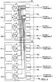
- Figure 4 is a diagram of two multiplexed test circuits parallel test equipment according to the invention.
- Test programming memory or main memory 10 contains the necessary instructions for the sequence functional test.
- the main memory 10 for test programming makes it possible to define the signal to generate for each pin. So, we define a elementary signal generation or comparison function, identical for each pin which, from the information contained in memory 10, generates stimuli, or signals of forcing, and receives response signals to compare with the data of table 18.
- test circuits each circuit being assigned to a spindle and comprising a set 22 of time generators controlling in parallel, on the one hand, a circuit 24 force, or event generator, sending forcing signals components located, for example, on two heads 1 and 2, and, on the other apart, a comparison circuit 26 receiving response signals heads 1 and 2 and comparing these signals with the data shown in table 18.
- the set 22 of time generators defines the times at which it is necessary to generate forcing signal fronts, the instants where you have to start comparing the response signals to the table 18 and the moments when we must stop comparing.
- the comparison circuit 26 performs a comparison, it generates a result, namely conforming or not conforming to the table. This result is specific to each spindle and to each component on which are made comparisons. In Figure 2, this result is indicated by “residue 1" for head 1 and by “residue 2" for head 2.
- a test circuit 20 in parallel of two components 1 and 2 comprises a set of time generators formed by four generators 22a , 22b, 22c, 22d intended to control circuits 24 1 , 24 2 by force and circuits 26 1 , 26 2 for comparison.
- Each force circuit 24 1 , 24 2 is capable of delivering a forcing signal on a given pin i of the components 1 and 2 to be tested.
- the response signal from each pin i is capable of being received by a respective comparison circuit 26 1 , 26 2 .
- circuits 22 la to 222d for time adjustment of the various test signals on a dynamic of the order of 5 ns.
- the time generators 22a, ... 22d are connected to the circuits 24 1 , 24 2 of force and to the circuits 26 1 , 26 2 of comparison so as to obtain forcing signals, on the one hand, and response signals, on the other hand, synchronous with one another, at a repetition frequency of 100 MHz for example.
- FIG. 3 illustrates a situation where the pins i of the electronic components 1 and 2 are not tested, the comparison circuits 26 1 , 26 2 not being used.
- FIG. 4 relates to an assembly in which a test circuit 20 of identical pins i of some parity is multiplexed to a circuit 20 'for testing identical pins i + 1 of opposite parity.
- the situation represented in FIG. 4 is the same as that of FIG. 1 in the sense that a single test signal, forcing for example, is applied to the only identical pins i of a given parity of the electronic components 1 and 2
- the circuits 24 1 , 24 2 of force of the test circuit 20 are then connected to all of the generators 22a, 22b, 22c, 22d; 22'a, 22'b, 22'c, 22'd of time so that the force signals are synchronous on said identical pins i of given parity of components 1 and 2.
- the repetition frequency of the signals is further doubled and this time reaches 400 MHz.
Landscapes
- Engineering & Computer Science (AREA)
- General Engineering & Computer Science (AREA)
- Physics & Mathematics (AREA)
- General Physics & Mathematics (AREA)
- Computer Networks & Wireless Communication (AREA)
- Computer Hardware Design (AREA)
- Microelectronics & Electronic Packaging (AREA)
- Tests Of Electronic Circuits (AREA)
- Test And Diagnosis Of Digital Computers (AREA)
Description
- un système de programmation,
- un circuit de test par broche comprenant un ensemble de génération de stimuli, ou signaux de forçage, qui doivent être appliqués à la broche considérée, et un ensemble de comparaison des signaux de réponse du composant,
- un ou plusieurs ensembles d'interface, têtes de mesure, permettant d'adapter les stimuli aux contraintes du composant que l'on veut vérifier.
- une instruction 14 qui est commune à l'ensemble des broches sous test et qui gère le déroulement de la mémoire principale. On nomme CALLM et RPTM des instructions d'appel de la séquence de mise en phase. Lorsque ces instructions sont invoquées, le circuit de mise en phase est activé et gère ainsi le déroulement de la mémoire principale 10 ou des sous-programmes. L'instruction RPTM exécute la même ligne jusqu'à ce que la mise en phase soit trouvée. L'instruction CALLM exécute une série d'instructions jusqu'à ce que la mise en phase soit trouvée. L'instruction CALLM boucle ainsi la mémoire. L'instruction INC consiste simplement à passer à la ligne suivante.
- la définition du type de temps 16 à utiliser pendant l'exécution de cette adresse de la mémoire. Le type de temps est commun pour l'ensemble des broches du testeur et correspond à l'adresse d'une mémoire qui est par broche et dans laquelle est définie la valeur des temps correspondant à cette adresse. Cette architecture de définition des temps correspond à l'architecture dite "séquenceur par broche" qui fait l'objet du brevet US n°5,212,443.
- une table 18 qui correspond au contenu logique (0 ou 1 par exemple) des signaux à envoyer ou à comparer. Cette table est par broche. Le testeur reçoit du composant sous test des signaux de réponse qu'il compare aux données de la table 18.
Claims (4)
- Procédé de test automatique en parallèle de composants électroniques, des broches identiques (i ; i + 1) desdits composants échangeant des signaux de test avec au moins un même circuit (20 ; 20') de test, lequel comporte, d'une part, des générateurs (22a, 22b, 22c, 22d ; 22'a, 22'b, 22'c, 22'd) de temps commandés par une mémoire (10) de programmation de test, et, d'autre part, des circuits (241, 242; 24'1, 24'2) de force et des circuits (261, 262 ; 26'1, 26'2) de comparaison contrôlés par lesdits générateurs de temps, caractérisé en ce que des générateurs de temps sont affectés soit auxdits circuits de force, soit auxdits circuits de comparaison, de manière à obtenir des signaux de test synchrones sur lesdites broches identiques (i) desdits composants électroniques.
- Équipement de test automatique en parallèle de composants électroniques, comprenant une pluralité de circuits (20, 20') de test associés respectivement à des broches (i; i+1) identiques desdits composants, chaque circuit (20 ; 20') de test comportant, d'une part, des générateurs (22a, 22b, 22c, 22d, 22'a, 22'b, 22'c, 22'd) de temps commandés par une mémoire (10) de programmation de test, et, d'autre part, des circuits (241, 242 ; 24'1, 24'2) de force et des circuits (261, 262 ; 26'1, 26'2) de comparaison contrôlés par lesdits générateurs de temps, caractérisé en ce que lesdits circuits de force, ou lesdits circuits de comparaison, d'au moins un circuit de test sont connectés à l'ensemble des générateurs de temps de manière à ce que les signaux de test soient synchrones sur lesdites broches identiques (i) desdits composants électroniques.
- Equipement selon la revendication 2, caractérisé en ce que les circuits (241, 242) de force, ou les circuits de comparaison, d'un même circuit (20) de test sont connectés à l'ensemble des générateurs (22a, 22b, 22c, 22d) de temps dudit circuit de test de manière que les signaux de test soient synchrones sur lesdites broches identiques (i) desdits composants électroniques.
- Equipement selon la revendication 2, dans lequel un circuit (20) de test de broches identiques (i) d'une certaine parité est multiplexé à un circuit (20') de test de broches identiques (i+1) de parité opposée, caractérisé en ce que les circuits (241, 242) de force, ou les circuits et comparaison, d'un même circuit (20) de test sont connectés à l'ensemble des générateurs (22a, 22b, 22c, 22d ; 22a', 22'b, 22'c, 22'd) de temps des circuits (20 ; 20') de test de manière que les signaux de test soient synchrones sur lesdites broches identiques (i) de parité donnée desdits composants électroniques.
Applications Claiming Priority (3)
| Application Number | Priority Date | Filing Date | Title |
|---|---|---|---|
| FR9504776A FR2733323B1 (fr) | 1995-04-19 | 1995-04-19 | Procede et equipement de test automatique en parallele de composants electroniques |
| FR9504776 | 1995-04-19 | ||
| PCT/FR1996/000541 WO1996033461A1 (fr) | 1995-04-19 | 1996-04-10 | Procede et equipement de test automatique en parallele de composants electroniques |
Publications (2)
| Publication Number | Publication Date |
|---|---|
| EP0823089A1 EP0823089A1 (fr) | 1998-02-11 |
| EP0823089B1 true EP0823089B1 (fr) | 2000-03-08 |
Family
ID=9478323
Family Applications (1)
| Application Number | Title | Priority Date | Filing Date |
|---|---|---|---|
| EP96912093A Expired - Lifetime EP0823089B1 (fr) | 1995-04-19 | 1996-04-10 | Procede et equipement de test automatique en parallele de composants electroniques |
Country Status (6)
| Country | Link |
|---|---|
| US (1) | US6049900A (fr) |
| EP (1) | EP0823089B1 (fr) |
| JP (1) | JPH11503831A (fr) |
| DE (1) | DE69606988T2 (fr) |
| FR (1) | FR2733323B1 (fr) |
| WO (1) | WO1996033461A1 (fr) |
Families Citing this family (13)
| Publication number | Priority date | Publication date | Assignee | Title |
|---|---|---|---|---|
| US6055661A (en) * | 1994-06-13 | 2000-04-25 | Luk; Fong | System configuration and methods for on-the-fly testing of integrated circuits |
| US6128727A (en) * | 1998-08-21 | 2000-10-03 | Advanced Micro Devices, Inc. | Self modifying code to test all possible addressing modes |
| JP3710639B2 (ja) * | 1999-02-24 | 2005-10-26 | 株式会社東芝 | 半導体装置 |
| US7842948B2 (en) * | 2004-02-27 | 2010-11-30 | Nvidia Corporation | Flip chip semiconductor die internal signal access system and method |
| US7279887B1 (en) * | 2004-08-06 | 2007-10-09 | Nvidia Corporation | In-process system level test before surface mount |
| US7810005B1 (en) * | 2006-11-01 | 2010-10-05 | Credence Systems Corporation | Method and system for correcting timing errors in high data rate automated test equipment |
| US8271252B2 (en) * | 2007-11-08 | 2012-09-18 | Nvidia Corporation | Automatic verification of device models |
| US8510616B2 (en) * | 2008-02-14 | 2013-08-13 | Nvidia Corporation | Scalable scan-based test architecture with reduced test time and test power |
| US8745200B2 (en) * | 2008-05-06 | 2014-06-03 | Nvidia Corporation | Testing operation of processors setup to operate in different modes |
| US8943457B2 (en) * | 2008-11-24 | 2015-01-27 | Nvidia Corporation | Simulating scan tests with reduced resources |
| WO2020042906A1 (fr) | 2018-08-31 | 2020-03-05 | Changxin Memory Technologies, Inc. | Procédés de test, testeur, plaque de charge et système de test |
| CN108732489B (zh) * | 2018-08-31 | 2023-09-05 | 长鑫存储技术有限公司 | 测试方法、测试设备、测试载板及测试系统 |
| TWI779586B (zh) * | 2021-04-30 | 2022-10-01 | 瑞昱半導體股份有限公司 | 測試電路系統的方法及相關電路系統 |
Family Cites Families (9)
| Publication number | Priority date | Publication date | Assignee | Title |
|---|---|---|---|---|
| US4928278A (en) * | 1987-08-10 | 1990-05-22 | Nippon Telegraph And Telephone Corporation | IC test system |
| US4972413A (en) * | 1989-03-23 | 1990-11-20 | Motorola, Inc. | Method and apparatus for high speed integrated circuit testing |
| US5025205A (en) * | 1989-06-22 | 1991-06-18 | Texas Instruments Incorporated | Reconfigurable architecture for logic test system |
| US5127011A (en) * | 1990-01-12 | 1992-06-30 | International Business Machines Corporation | Per-pin integrated circuit test system having n-bit interface |
| JP2854659B2 (ja) * | 1990-03-20 | 1999-02-03 | 三菱電機株式会社 | 半導体装置のテスト装置 |
| US5225772A (en) * | 1990-09-05 | 1993-07-06 | Schlumberger Technologies, Inc. | Automatic test equipment system using pin slice architecture |
| DE59010430D1 (de) * | 1990-12-28 | 1996-08-29 | Ibm | Programmgesteuertes Verfahren und Anordnung zur Erzeugung von Impulsen in aufeinanderfolgenden Impulsintervallen |
| DE69502827T2 (de) * | 1995-08-10 | 1998-10-15 | Hewlett Packard Gmbh | Elektronischer Schaltungs- oder Kartenprüfer und Verfahren zur Prüfung einer elektronischen Vorrichtung |
| US5835506A (en) * | 1997-04-29 | 1998-11-10 | Credence Systems Corporation | Single pass doublet mode integrated circuit tester |
-
1995
- 1995-04-19 FR FR9504776A patent/FR2733323B1/fr not_active Expired - Fee Related
-
1996
- 1996-04-10 JP JP8531508A patent/JPH11503831A/ja not_active Ceased
- 1996-04-10 EP EP96912093A patent/EP0823089B1/fr not_active Expired - Lifetime
- 1996-04-10 WO PCT/FR1996/000541 patent/WO1996033461A1/fr not_active Ceased
- 1996-04-10 DE DE69606988T patent/DE69606988T2/de not_active Expired - Fee Related
- 1996-04-10 US US08/930,492 patent/US6049900A/en not_active Expired - Fee Related
Also Published As
| Publication number | Publication date |
|---|---|
| FR2733323A1 (fr) | 1996-10-25 |
| DE69606988T2 (de) | 2000-10-05 |
| WO1996033461A1 (fr) | 1996-10-24 |
| EP0823089A1 (fr) | 1998-02-11 |
| FR2733323B1 (fr) | 1997-05-30 |
| US6049900A (en) | 2000-04-11 |
| JPH11503831A (ja) | 1999-03-30 |
| DE69606988D1 (de) | 2000-04-13 |
Similar Documents
| Publication | Publication Date | Title |
|---|---|---|
| EP0823089B1 (fr) | Procede et equipement de test automatique en parallele de composants electroniques | |
| WO1993024881A1 (fr) | Procede et plate-formes de test pour le developpement d'un circuit integre | |
| EP0146661B1 (fr) | Procédé de diagnostic électrique pour identifier une cellule défectueuse dans une chaîne de cellules formant un registre à décalage | |
| EP0104293A1 (fr) | Dispositif pour le chargement et la lecture de différentes chaînes de bascules dans un système de traitement de données | |
| EP0578540B1 (fr) | Procédé pour tester le fonctionnement d'un circuit intégré spécialisé, et circuit intégré spécialisé s'y rapportant | |
| EP3625579B1 (fr) | Appareil de test et procede de test d'un circuit integre | |
| EP0820613B1 (fr) | Procede et equipement de test automatique en parallele de composants electroniques | |
| EP0939372B1 (fr) | Dispositif de test en production des caractéristiques dynamiques de composants utilisant des transmissions série | |
| FR2724030A1 (fr) | Procede de selection automatique de qualificateurs d'impulsions d'horloge dans des systemes d'emulation de materiel reprogrammable | |
| FR3033412A1 (fr) | Testeur de circuits integres sur une galette de silicium et circuit integre. | |
| EP0823088B1 (fr) | Procede et equipement de test automatique en parallele de composants electroniques | |
| FR2658933A1 (fr) | Systeme de commande du deroulement de sequences de tests dans un appareil de traitement de l'information. | |
| EP1159628B1 (fr) | Procede de test de circuits integres avec acces a des points de memorisation du circuit | |
| FR2754904A1 (fr) | Production d'impulsions dans le canal analogique d'un appareil de test automatique | |
| FR2498782A1 (fr) | Systeme de traitement de l'information | |
| EP1813952B1 (fr) | Test de scan | |
| FR2870955A1 (fr) | Debogueur d'un circuit electronique fabrique a partir d'un programme en langage de description de materiel | |
| WO2000029953A1 (fr) | Procede et installation de localisation rapide d'un defaut dans un circuit integre | |
| EP0800676B1 (fr) | Procede et equipement de test automatique de composants electroniques | |
| FR2800169A1 (fr) | Procede et dispositif d'analyse de defauts dans des circuits logiques numeriques | |
| WO2006120315A1 (fr) | Circuit integre comportant un mode de test securise par detection de l’etat chaine des cellules configurables du circuit integre | |
| EP1324061A2 (fr) | Procédé de test d'un circuit integré par simulation | |
| FR3031820A1 (fr) | Procede de determination de la validite d'un modele | |
| FR2752967A1 (fr) | Procede de developpement d'un circuit integre specifique d'une application (asic) et emulateur correspondant | |
| FR2906891A1 (fr) | Registre scan parametrique, circuit numerique et procede de test d'un circuit numerique a l'aide d'un tel registre |
Legal Events
| Date | Code | Title | Description |
|---|---|---|---|
| PUAI | Public reference made under article 153(3) epc to a published international application that has entered the european phase |
Free format text: ORIGINAL CODE: 0009012 |
|
| 17P | Request for examination filed |
Effective date: 19970917 |
|
| AK | Designated contracting states |
Kind code of ref document: A1 Designated state(s): DE FR GB IT NL SE |
|
| RAP1 | Party data changed (applicant data changed or rights of an application transferred) |
Owner name: SCHLUMBERGER SYSTEMES |
|
| GRAG | Despatch of communication of intention to grant |
Free format text: ORIGINAL CODE: EPIDOS AGRA |
|
| GRAG | Despatch of communication of intention to grant |
Free format text: ORIGINAL CODE: EPIDOS AGRA |
|
| GRAH | Despatch of communication of intention to grant a patent |
Free format text: ORIGINAL CODE: EPIDOS IGRA |
|
| 17Q | First examination report despatched |
Effective date: 19990701 |
|
| GRAH | Despatch of communication of intention to grant a patent |
Free format text: ORIGINAL CODE: EPIDOS IGRA |
|
| GRAA | (expected) grant |
Free format text: ORIGINAL CODE: 0009210 |
|
| AK | Designated contracting states |
Kind code of ref document: B1 Designated state(s): DE FR GB IT NL SE |
|
| GBT | Gb: translation of ep patent filed (gb section 77(6)(a)/1977) |
Effective date: 20000308 |
|
| REF | Corresponds to: |
Ref document number: 69606988 Country of ref document: DE Date of ref document: 20000413 |
|
| ITF | It: translation for a ep patent filed | ||
| PLBE | No opposition filed within time limit |
Free format text: ORIGINAL CODE: 0009261 |
|
| STAA | Information on the status of an ep patent application or granted ep patent |
Free format text: STATUS: NO OPPOSITION FILED WITHIN TIME LIMIT |
|
| 26N | No opposition filed | ||
| REG | Reference to a national code |
Ref country code: GB Ref legal event code: IF02 |
|
| PGFP | Annual fee paid to national office [announced via postgrant information from national office to epo] |
Ref country code: SE Payment date: 20020405 Year of fee payment: 7 |
|
| PGFP | Annual fee paid to national office [announced via postgrant information from national office to epo] |
Ref country code: GB Payment date: 20020410 Year of fee payment: 7 |
|
| PGFP | Annual fee paid to national office [announced via postgrant information from national office to epo] |
Ref country code: DE Payment date: 20020417 Year of fee payment: 7 |
|
| PGFP | Annual fee paid to national office [announced via postgrant information from national office to epo] |
Ref country code: FR Payment date: 20020425 Year of fee payment: 7 |
|
| PGFP | Annual fee paid to national office [announced via postgrant information from national office to epo] |
Ref country code: NL Payment date: 20020426 Year of fee payment: 7 |
|
| REG | Reference to a national code |
Ref country code: FR Ref legal event code: ST |
|
| PG25 | Lapsed in a contracting state [announced via postgrant information from national office to epo] |
Ref country code: GB Free format text: LAPSE BECAUSE OF NON-PAYMENT OF DUE FEES Effective date: 20030410 |
|
| PG25 | Lapsed in a contracting state [announced via postgrant information from national office to epo] |
Ref country code: SE Free format text: LAPSE BECAUSE OF NON-PAYMENT OF DUE FEES Effective date: 20030411 |
|
| PG25 | Lapsed in a contracting state [announced via postgrant information from national office to epo] |
Ref country code: NL Free format text: LAPSE BECAUSE OF NON-PAYMENT OF DUE FEES Effective date: 20031101 Ref country code: DE Free format text: LAPSE BECAUSE OF NON-PAYMENT OF DUE FEES Effective date: 20031101 |
|
| NLV4 | Nl: lapsed or anulled due to non-payment of the annual fee |
Effective date: 20031101 |
|
| EUG | Se: european patent has lapsed | ||
| GBPC | Gb: european patent ceased through non-payment of renewal fee |
Effective date: 20030410 |
|
| PG25 | Lapsed in a contracting state [announced via postgrant information from national office to epo] |
Ref country code: IT Free format text: LAPSE BECAUSE OF NON-PAYMENT OF DUE FEES;WARNING: LAPSES OF ITALIAN PATENTS WITH EFFECTIVE DATE BEFORE 2007 MAY HAVE OCCURRED AT ANY TIME BEFORE 2007. THE CORRECT EFFECTIVE DATE MAY BE DIFFERENT FROM THE ONE RECORDED. Effective date: 20050410 |
|
| PG25 | Lapsed in a contracting state [announced via postgrant information from national office to epo] |
Ref country code: FR Free format text: LAPSE BECAUSE OF NON-PAYMENT OF DUE FEES Effective date: 20030430 |