EP0823736A2 - Transistor bipolaire vertical et méthode de fabrication - Google Patents
Transistor bipolaire vertical et méthode de fabrication Download PDFInfo
- Publication number
- EP0823736A2 EP0823736A2 EP97250228A EP97250228A EP0823736A2 EP 0823736 A2 EP0823736 A2 EP 0823736A2 EP 97250228 A EP97250228 A EP 97250228A EP 97250228 A EP97250228 A EP 97250228A EP 0823736 A2 EP0823736 A2 EP 0823736A2
- Authority
- EP
- European Patent Office
- Prior art keywords
- layer
- comb
- polysilicon
- trench
- emitter
- Prior art date
- Legal status (The legal status is an assumption and is not a legal conclusion. Google has not performed a legal analysis and makes no representation as to the accuracy of the status listed.)
- Withdrawn
Links
Images


Classifications
-
- H—ELECTRICITY
- H10—SEMICONDUCTOR DEVICES; ELECTRIC SOLID-STATE DEVICES NOT OTHERWISE PROVIDED FOR
- H10D—INORGANIC ELECTRIC SEMICONDUCTOR DEVICES
- H10D10/00—Bipolar junction transistors [BJT]
- H10D10/01—Manufacture or treatment
- H10D10/051—Manufacture or treatment of vertical BJTs
- H10D10/056—Manufacture or treatment of vertical BJTs of vertical BJTs having the main current going through the whole substrate, e.g. power BJTs
- H10D10/058—Manufacture or treatment of vertical BJTs of vertical BJTs having the main current going through the whole substrate, e.g. power BJTs having multi-emitter structures, e.g. interdigitated, multi-cellular or distributed emitters
-
- H—ELECTRICITY
- H10—SEMICONDUCTOR DEVICES; ELECTRIC SOLID-STATE DEVICES NOT OTHERWISE PROVIDED FOR
- H10D—INORGANIC ELECTRIC SEMICONDUCTOR DEVICES
- H10D10/00—Bipolar junction transistors [BJT]
-
- H—ELECTRICITY
- H10—SEMICONDUCTOR DEVICES; ELECTRIC SOLID-STATE DEVICES NOT OTHERWISE PROVIDED FOR
- H10D—INORGANIC ELECTRIC SEMICONDUCTOR DEVICES
- H10D62/00—Semiconductor bodies, or regions thereof, of devices having potential barriers
- H10D62/10—Shapes, relative sizes or dispositions of the regions of the semiconductor bodies; Shapes of the semiconductor bodies
- H10D62/113—Isolations within a component, i.e. internal isolations
- H10D62/115—Dielectric isolations, e.g. air gaps
-
- H—ELECTRICITY
- H10—SEMICONDUCTOR DEVICES; ELECTRIC SOLID-STATE DEVICES NOT OTHERWISE PROVIDED FOR
- H10D—INORGANIC ELECTRIC SEMICONDUCTOR DEVICES
- H10D62/00—Semiconductor bodies, or regions thereof, of devices having potential barriers
- H10D62/10—Shapes, relative sizes or dispositions of the regions of the semiconductor bodies; Shapes of the semiconductor bodies
- H10D62/13—Semiconductor regions connected to electrodes carrying current to be rectified, amplified or switched, e.g. source or drain regions
- H10D62/137—Collector regions of BJTs
-
- H—ELECTRICITY
- H10—SEMICONDUCTOR DEVICES; ELECTRIC SOLID-STATE DEVICES NOT OTHERWISE PROVIDED FOR
- H10D—INORGANIC ELECTRIC SEMICONDUCTOR DEVICES
- H10D64/00—Electrodes of devices having potential barriers
- H10D64/20—Electrodes characterised by their shapes, relative sizes or dispositions
- H10D64/23—Electrodes carrying the current to be rectified, amplified, oscillated or switched, e.g. sources, drains, anodes or cathodes
- H10D64/231—Emitter or collector electrodes for bipolar transistors
-
- H—ELECTRICITY
- H10—SEMICONDUCTOR DEVICES; ELECTRIC SOLID-STATE DEVICES NOT OTHERWISE PROVIDED FOR
- H10D—INORGANIC ELECTRIC SEMICONDUCTOR DEVICES
- H10D64/00—Electrodes of devices having potential barriers
- H10D64/60—Electrodes characterised by their materials
- H10D64/62—Electrodes ohmically coupled to a semiconductor
Definitions
- the invention relates to a vertical bipolar transistor according to the preamble of the main claim and a process for its manufacture.
- the invention has for its object a vertical Bipolar transistor for high frequency and To create high performance area, its characteristics such as dielectric strength or frequency behavior improved over the prior art are and which has a high packing density. A process for its production is also intended to provide.
- a comb-like isolation trench and a comb-like collector layer is provided, wherein the "teeth" of the comb-like formation of the collector layer and the isolation trench.
- the isolation trench this is the very center of the transistor close and has an excellent thermal conductivity, whereby the heat from the center of the transistor can be easily removed. So there is one uniform temperature distribution and the collector transition has a relatively low temperature. Due to the increased circumferential length compared to the prior art the internal resistance to the surfaces of the collector of the transistor will be lowered and it will the warm stability of the transistor when increasing the Output line improved.
- the isolation trench Due to the isolation trench according to the invention Space charge zone of the collector completely in one Deep trapping included, i.e. the isolation trench extends so far into the substrate that at each any counter-bias to breakdown voltage down that generated before this counter-bias Space charge area included in the deep trap is. You can therefore no longer laterally the surface achieve, whereby surface effects by the Space charge zones of the collector can be avoided. In particular, this improves the parasitic ones Parameters of the bipolar transistor according to the invention. By including the space charge zone in the called deep catch is in the collector layer of the Transistor generates a homogeneous electric field, which is no longer to the side of the transistor Surface of the substrate is curved. This does not occur Field strength peaks more and there is one higher dielectric strength of the invention Transistor.
- the isolation trench is directly adjacent to the collector and also to the base, whereby the lateral curved transition areas between the base and collector are eliminated, thereby eliminating the Breakdown voltage at the collector transition considerably can be increased.
- the result is a better one Relationship between the area of the emitter base contact and the area of the base collector contact. This also leads to the transistor according to the invention a larger current and a greater output can deliver.
- the arrangement according to the invention a higher doping of the transistor layers and consequently also a higher current density for a given Dielectric strength possible.
- the higher doping allows a higher cut-off frequency, where the transistor is still operating reliably can be because the space charge zone at higher Doping compared to the prior art is less extensive.
- the bipolar transistor according to the invention particularly as a high-performance component and as a high-frequency component for everyone conceivable application.
- the bipolar transistor according to the invention has no protective rings and therefore has a considerably smaller area requirement compared to the prior art.
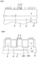
- the isolation trench 5 replaces the previously known ring protection technology (see FIG. 8), by means of which high voltage resistance is to be achieved.
- Fig. 9 which shows a section through part of the bipolar transistor according to the invention, shows that the use of the isolation trench reduces the functional area SC 'of the collector transition zone of the transistor (S C' ⁇ S C ). This increases the cutoff frequency of the transistor.
- FIG. 9 shows that as the width W G of the trench increases, the bottom surface S G of the trench increases. The functional area S C ' is not changed.
- the process according to the invention can be carried out in particular combine very well with a self-adjusting procedure, whereby particularly plane-parallel emitter-base or base-collector contact surfaces are produced will.
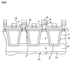
- a vertical bipolar transistor for the high-power and high-frequency range which has an n-doped emitter layer 2, a p-doped base layer 3 and an n-doped collector layer 4 in a vertical layer sequence and incorporated into a substrate 11.
- the emitter 2 is contacted via a conductive layer 6 on the surface of the substrate 11 and the base 3 has a contact 8 via a p + -doped region 7.
- the conductive layer 6 representing the contact and the contact 8 are via an insulating layer 10 separated from each other.
- the vertical bipolar transistor is laterally delimited by a vertical isolation trench 5 which extends from the surface of the substrate at its depth.
- the walls of the isolation trench 5 are formed by an insulating SiO 2 layer and the interior between the trench walls 12 is filled with polysilicon as filler 9.
- the bipolar transistor has a comb-like or finger-like structure, the different Layers drawn in dashed lines in Fig. 1A are.
- the bipolar transistor has another middle isolation trench 5, which in Fig. 1C to is recognizable.
- the inside and outside of the walls 12 of the middle isolation trench 5 (E), which the Facing emitter 3 are 12a (E) and 12b (E) designated.
- the reference numerals 20 (B and 20 (E) place the electrodes on the base and on the emitter, which in this case is made of aluminum consist. All electrodes form a multilayer Electrode system 18, 19, 20, below be described in more detail.
- Reference numeral 26 represents a base contact window.
- the collector 4 and the isolation trench 5 both of which are comb-like, interlock, this comb-like collector and the comb-like isolation trench being a special feature of this invention.
- Figs. 4A to 4G the manufacture of the transistor is explained in more detail.
- the upper surface of the isolation trench 5 is covered with p + -doped polysilicon as contact 8.
- 4B that the comb-like isolation trench 5 is self-aligned by means of the p + -doped polysilicon 8 with the comb-like collector 4.
- the isolation trench 5 is connected directly to the comb-like collector 4, it being further essential for the invention that the width of the arm or "prong" of the comb-like isolation trench 5 W G is wider than the corresponding part of the comb-like collector W C.
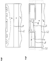
- the depth of the comb-like isolation trench 5 D G should be at least 2 ⁇ m greater than the depth of the space charge zone, the limit of which is indicated by reference numeral 56, this limit applying to a voltage which is just below the breakdown voltage. Overall, the depth of the comb-like isolation trench is preferably 5 ⁇ D G ⁇ 17 ⁇ m. The deeper the isolation trench, the more the parasite resistance of the isolation trench can be reduced. Too great a depth is not favorable for the heat dissipation of the collector 4. The difference of 2 ⁇ m is an optimal value.
- the substrate 11 is formed from several layers.
- a single crystal n + semiconductor substrate 55 is provided which is doped with As or Sb.
- An n-epitaxial layer 14 doped with As is formed on this n + Si substrate 55, on which a further n - epitaxial layer 4 doped with As is formed.
- These three layers form a semiconductor substrate 11 (see FIG. 4C).
- Three insulation layers 15, 16, 17, a thin SiO 2 layer 15, a SiN layer 16 and a thick SiO 2 layer 17 are produced in succession on this semiconductor substrate. Comb-like insulation windows A, B , C, D, which reveal the n - epitaxial layer 4.
- the n - epitaxial layer 4 is etched through to the surface of the n epitaxial layer 14 using the RIE etching method, as a result of which the isolation trench 5 is formed.
- an SiO 2 insulation film is formed on the inner wall 12b (C) of the comb-like isolation trench 5.
- polysilicon is deposited in the trench and fills it , whereby the comb-like isolation trench 5 is formed.
- the remnants of the Si layer are removed using the CMP method and the SiN layer 16 is used as a cover in order to etch away the polysilicon located in the isolation trench by 300 nm.
- an SiO 2 insulation layer is formed on the upper surface of the comb-like insulation trench 5, so that a trench is formed all around by the walls 12.
- the three insulation layers (FIG. 4C) 15, 16, 17 are then wet-etched away and, according to FIG. 4E, a p + polysilicon layer 8, an SiO 2 layer 26 and an SiN layer 27 are deposited on the entire semiconductor substrate.
- a structure made of p + polysilicon 8 / SiO 2 26 / SiN is formed, which matches the finger image of the comb-like isolation trench 5.
- the comb-like collector transition is formed in a self-adjusted manner by the diffusion of boron atoms contained in the p + polysilicon into the n - epitaxial layer 4 and by the boron ion implantation, the transition surface of the comb-like collector abutting the side walls 12 of the comb-like trench 5 at right angles.
- the outer base electrode zone 7 is also formed by diffusion of the boron atoms in the p + polysilicon.
- an SiO 2 film which contains B is first deposited.
- the side wall of the emitter 2 is then formed using the RIE method and self-adjustment.
- the SiN film is then removed using H 3 PO 4 .
- a polysilicon layer doped with As is deposited, with the aid of masks and the RIE method the polysilicon emitter doped with As is produced, which likewise has a comb-shaped structure.
- the p + polysilicon layer is then etched and a connection window is formed in accordance with FIG. 4G-B.
- a 100 nm thick Ti layer is deposited and a subsequent RTA process produces a TiSi 2 layer in a self-aligned manner on the p + polysilicon layer in the base connection opening and on the As doped polysilicon layer of the emitter, as a result of which the polysilicon / TiSi 2 Emitter is formed.
- a TiSi 2 forms in the contact window of the base electrode and on the polysilicon emitter doped with As, with self-adjustment.
- the unreactive Ti is removed with solvent of NH 4 OH / H 2 O 2 / H 2 O and, with the deposition of a TiN layer and an AlSiCu layer or gold layer, a multilayer metallized electrode system made of doped polysilicon TiSi 2 / TiN / AlSiCu is formed. In this way, the vertical bipolar transistor with a comb-like collector is produced, the emitter having a width of 72 ⁇ m.
- Figs. 1 and 4 shown vertical bipolar transistor is using a self-adjusting procedure produced. This allows plane-parallel transitions between emitter 2 and base 3 and between Base 3 and collector 4 are generated. The plane parallelism of these interfaces between different doped layers enables a special homogeneous electric field across the transistor.
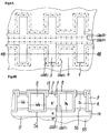
- Fig. 2 shows a further embodiment of the vertical bipolar transistor.
- the transistor shown in Fig. 2 also has a comb-like isolation trench 5, to the base layer 3 and collector layer 4 oriented side walls 12 in the direction of the depth of the substrate 11 run towards each other and at a certain angle ⁇ are inclined to the vertical. This narrows the cross section of the collector 4 in depth of the substrate 11 progressively, thereby including the Space charge area of the collector further improved becomes.
- the figures 5A to 5C show the method steps for producing the embodiment according to FIG. 2.
- 5A shows that a thin SiO 2 layer 21 forms on n-epitaxial layer 14.
- An Si 3 N 4 layer 22 is deposited using the CVD process, so that a two-layer thin structure is formed.
- Epitaxial polysilicon is grown on this structure as the filling material 9, the thickness of which lies between 5 and 17 ⁇ m.
- a thick SiO 2 layer 23 is deposited on this polysilicon layer 9 using the CVD method, and is structured like a comb with the aid of the mask and etching method, as a result of which the polysilicon layer is exposed.
- the polysilicon layer 9 located in the comb-like window is etched until the SiN 4 layer 22 is exposed. Then the SiO 2 layer 23 is wet-etched away, at the same time the trapezoidal surface made of polysilicon 9 forms with the angle of inclination.
- the trapezoidal walls 12 made of SiO 2 are formed on the polysilicon 9. 5B, the Si 3 N 4 layer 22 is etched with hot H 3 PO 4 and the SiO 2 layer 21 is etched with dilute BHF, as a result of which the n-epitaxial layer 14 is exposed.
- Fig. 3 shows a further embodiment of the vertical Bipolar transistor.
- the side walls 12 of the isolation trench 5 the Base 2 and the collector 4 are facing, against the Vertical inclined at a certain angle ⁇ so that they are in the direction of the depth of the substrate 11 diverge.
- ⁇ the vertical inclined at a certain angle ⁇ so that they are in the direction of the depth of the substrate 11 diverge.
- the cross section of the collector 4 in depth of the substrate 11, resulting in improved heat dissipation take place from the collector area 4 to the substrate can.
- FIG. 6A shows that a semiconductor substrate is initially provided, which consists of an n + silicon layer 55, an n epitaxial layer 14 and an n - epitaxial layer 4.
- a three-layer insulation structure made of thin SiO 2 15, an Si 3 N 4 layer 16 and a thick SiO 2 layer 17 is deposited on the n - epitaxial layer 4 using the CVD method.
- This three-layer insulation structure is provided with windows through which etching takes place, to the n-epitaxial layer 14. This creates an oblique comb-like trench with the desired angle of inclination.
- an SiO 2 insulation layer is formed on the inner wall of the comb-like oblique trench using the LOCOS method and undoped polysilicon is deposited using the LPCVD method and fills the trench.
- the CMP process removes the undoped polysilicon layer on the Si 3 N 4 layer 16 so that the surface becomes smooth.
- the approximately 300 nm-thick undoped polysilicon is then wet-etched away on the surface of the comb-like oblique trench.
- the SiO 2 layer forms on the surface of the comb-like oblique trench, whereupon the Si 3 N 4 layer 16 is removed by means of H 3 PO 4 and then the layer 15.
- FIG. 6C the further steps of the manufacturing method of the comb-type bipolar transistor are identical to those shown in FIG. 4.
- Figs. 7A to 7C are the process steps for producing the polysilicon / TiSi 2 emitter doped with As, the finger width of the emitter being less than 2 ⁇ m and the length being greater than 10 ⁇ m.
- 7A shows the plan of the vertical transistor, 18 (B) the TiSi 2 layer on the comb-like finger of the base electrode, 18 (E) the TiSi 2 layer of the emitter, 20 (B) the Al electrode of the Base electrode and 20 (E) mean the Al electrode of the emitter electrode.
- 5 (C) denote the comb-like isolation trench essentially in the collector area and 5 (E) the isolation trench of the emitter zone.
- the width of the isolation trench 5 (E) is 0.5 to 3 ⁇ m, the depth is 0.5 to 15 ⁇ m.
- the isolation trench 5 (E) has the function of reducing C TE from the emitter junction.
- contact openings of the base are produced on the p + polysilicon 8 and the SiO 2 layer 26.
- a Ti layer with a thickness of approximately 100 nm is then deposited on the entire surface of the semiconductor substrate.
- the TI layer is treated by an RTA process at temperatures of 500 to 600 ° C., so that TiSi is formed on the polysilicon surface.
- the unreacted Ti or the TiN formed during the RTA treatment is etched away, and on the surface formed with p + polysilicon and polysilicon, for example, TiSi is formed at high temperatures 750 ° C under N 2 protection converted into TiSi 2 using the RTA process.
- an SiO 2 layer 27 is first deposited on the entire surface, then this is etched using a mask and the RIE method, so that contact windows of the base and the emitter are formed.
- a multilayered metallized structure TiN / Ti / AlSiCu / or Au is then deposited.
- a multilayer metallized system polysilicon / TiSi / TiN / AlSiCu is produced with high reliability.
Landscapes
- Bipolar Transistors (AREA)
Applications Claiming Priority (2)
| Application Number | Priority Date | Filing Date | Title |
|---|---|---|---|
| DE19632412 | 1996-08-05 | ||
| DE19632412A DE19632412A1 (de) | 1996-08-05 | 1996-08-05 | Vertikaler Bipolartransistor und Verfahren zu seiner Herstellung |
Publications (2)
| Publication Number | Publication Date |
|---|---|
| EP0823736A2 true EP0823736A2 (fr) | 1998-02-11 |
| EP0823736A3 EP0823736A3 (fr) | 1999-07-21 |
Family
ID=7802385
Family Applications (1)
| Application Number | Title | Priority Date | Filing Date |
|---|---|---|---|
| EP97250228A Withdrawn EP0823736A3 (fr) | 1996-08-05 | 1997-08-05 | Transistor bipolaire vertical et méthode de fabrication |
Country Status (2)
| Country | Link |
|---|---|
| EP (1) | EP0823736A3 (fr) |
| DE (1) | DE19632412A1 (fr) |
Cited By (3)
| Publication number | Priority date | Publication date | Assignee | Title |
|---|---|---|---|---|
| WO2004102670A2 (fr) | 2003-05-13 | 2004-11-25 | Koninklijke Philips Electronics N.V. | Dispositifs a semi-conducteurs pourvus d'une zone de formation de champ |
| CN100492656C (zh) * | 2003-05-13 | 2009-05-27 | Nxp股份有限公司 | 具有场整形区的半导体器件 |
| CN111009574A (zh) * | 2018-10-08 | 2020-04-14 | 意法半导体有限公司 | 双极晶体管 |
Families Citing this family (1)
| Publication number | Priority date | Publication date | Assignee | Title |
|---|---|---|---|---|
| DE10042343C2 (de) * | 2000-08-29 | 2002-10-10 | Infineon Technologies Ag | Bipolartransistor in einer vertikalen strukturierten Schichtenfolge, Verfahren zu seiner Herstellung und Verwendung eines solchen |
Family Cites Families (10)
| Publication number | Priority date | Publication date | Assignee | Title |
|---|---|---|---|---|
| US4159915A (en) * | 1977-10-25 | 1979-07-03 | International Business Machines Corporation | Method for fabrication vertical NPN and PNP structures utilizing ion-implantation |
| US4269636A (en) * | 1978-12-29 | 1981-05-26 | Harris Corporation | Method of fabricating self-aligned bipolar transistor process and device utilizing etching and self-aligned masking |
| JPS61208869A (ja) * | 1985-03-14 | 1986-09-17 | Nec Corp | 半導体装置及びその製造方法 |
| NL8503408A (nl) * | 1985-12-11 | 1987-07-01 | Philips Nv | Hoogfrequenttransistor en werkwijze ter vervaardiging daarvan. |
| US4829015A (en) * | 1987-05-21 | 1989-05-09 | Siemens Aktiengesellschaft | Method for manufacturing a fully self-adjusted bipolar transistor |
| JPS6436065A (en) * | 1987-07-31 | 1989-02-07 | Nec Corp | Bipolar type semiconductor device |
| US5164218A (en) * | 1989-05-12 | 1992-11-17 | Nippon Soken, Inc. | Semiconductor device and a method for producing the same |
| DE59108607D1 (de) * | 1990-09-20 | 1997-04-17 | Siemens Ag | Bipolartransistor für hohe Leistung im Mikrowellenlängenbereich |
| DE4211050C2 (de) * | 1992-04-02 | 1995-10-19 | Siemens Ag | Verfahren zur Herstellung eines Bipolartransistors in einem Substrat |
| JP2914117B2 (ja) * | 1993-08-28 | 1999-06-28 | 日本電気株式会社 | 半導体装置の製造方法 |
-
1996
- 1996-08-05 DE DE19632412A patent/DE19632412A1/de not_active Ceased
-
1997
- 1997-08-05 EP EP97250228A patent/EP0823736A3/fr not_active Withdrawn
Cited By (8)
| Publication number | Priority date | Publication date | Assignee | Title |
|---|---|---|---|---|
| WO2004102670A2 (fr) | 2003-05-13 | 2004-11-25 | Koninklijke Philips Electronics N.V. | Dispositifs a semi-conducteurs pourvus d'une zone de formation de champ |
| WO2004102670A3 (fr) * | 2003-05-13 | 2005-01-20 | Koninkl Philips Electronics Nv | Dispositifs a semi-conducteurs pourvus d'une zone de formation de champ |
| US7423299B2 (en) | 2003-05-13 | 2008-09-09 | Nxp B.V. | Semiconductor devices with a field shaping region |
| CN100492656C (zh) * | 2003-05-13 | 2009-05-27 | Nxp股份有限公司 | 具有场整形区的半导体器件 |
| CN111009574A (zh) * | 2018-10-08 | 2020-04-14 | 意法半导体有限公司 | 双极晶体管 |
| US11837647B2 (en) | 2018-10-08 | 2023-12-05 | Stmicroelectronics (Crolles 2) Sas | Bipolar transistor |
| CN111009574B (zh) * | 2018-10-08 | 2024-01-30 | 意法半导体有限公司 | 双极晶体管 |
| US12125894B2 (en) | 2018-10-08 | 2024-10-22 | Stmicroelectronics (Crolles 2) Sas | Bipolar transistor |
Also Published As
| Publication number | Publication date |
|---|---|
| EP0823736A3 (fr) | 1999-07-21 |
| DE19632412A1 (de) | 1998-02-12 |
Similar Documents
| Publication | Publication Date | Title |
|---|---|---|
| DE10203164B4 (de) | Leistungshalbleiterbauelement und Verfahren zu dessen Herstellung | |
| DE19807745B4 (de) | Halbleitereinrichtung und Herstellungsverfahren einer Halbleitereinrichtung | |
| DE69315239T2 (de) | VDMOS-Transistor mit verbesserter Durchbruchsspannungscharakteristik | |
| DE60125784T2 (de) | Graben-mosfet-struktur mit geringer gate-ladung | |
| DE69525592T2 (de) | Graben-dmos-transistor mit kanalblockierer in den zellgrabenecken | |
| DE4220497B4 (de) | Halbleiterspeicherbauelement und Verfahren zu dessen Herstellung | |
| DE2212049C2 (de) | Verfahren zur Herstellung einer Halbleiteranordnung und Verfahren zur Herstellung eines Transistors | |
| DE4445345C2 (de) | Verfahren zur Herstellung eines Bipolartransistors | |
| DE2646308C3 (de) | Verfahren zum Herstellen nahe beieinander liegender elektrisch leitender Schichten | |
| DE68927353T2 (de) | Verfahren zur Herstellung einer Planarisolierung | |
| DE102005041108B3 (de) | Verfahren zur Herstellung eines Trench-Transistors und Trench-Transistor | |
| DE102010000113B4 (de) | Halbleiterbauelement und Verfahren zur Herstellung | |
| DE2502235A1 (de) | Ladungskopplungs-halbleiteranordnung | |
| DE10101568A1 (de) | Halbleitervorrichtung und Verfahren zur Herstellung derselben | |
| DE10234996B4 (de) | Verfahren zur Herstellung einer Transistoranordnung mit Trench-Transistorzellen mit Feldelektrode | |
| DE102005018378B4 (de) | Halbleitervorrichtung der Bauart mit dielektrischer Isolierung | |
| DE102009002813B4 (de) | Verfahren zur Herstellung eines Transistorbauelements mit einer Feldplatte | |
| DE19853268C2 (de) | Feldeffektgesteuerter Transistor und Verfahren zu dessen Herstellung | |
| DE10229653A1 (de) | Halbleitervorrichtung und Verfahren zu ihrer Harstellung | |
| DE2824419A1 (de) | Halbleitervorrichtung und verfahren zu deren herstellung | |
| DE10129289A1 (de) | Halbleitervorrichtung mit einer Diode für eine Eingangschutzschaltung einer MOS-Vorrichtung und Verfahren zu deren Herstellung | |
| EP0000545B1 (fr) | Procédé de fabrication d'un dispositif semiconducteur à auto-alignement | |
| EP1631990B1 (fr) | Procede de fabrication d'un transistor a effet de champ | |
| DE19634178C2 (de) | Verfahren zur Herstellung eines bipolaren Halbleiterbauteils | |
| DE10261600B4 (de) | Halbleiterbauteil und Verfahren zu seiner Herstellung |
Legal Events
| Date | Code | Title | Description |
|---|---|---|---|
| PUAI | Public reference made under article 153(3) epc to a published international application that has entered the european phase |
Free format text: ORIGINAL CODE: 0009012 |
|
| AK | Designated contracting states |
Kind code of ref document: A2 Designated state(s): AT BE CH DE DK ES FI FR GB GR IE IT LI LU MC NL PT SE |
|
| AX | Request for extension of the european patent |
Free format text: AL;LT;LV;RO;SI |
|
| PUAL | Search report despatched |
Free format text: ORIGINAL CODE: 0009013 |
|
| AK | Designated contracting states |
Kind code of ref document: A3 Designated state(s): AT BE CH DE DK ES FI FR GB GR IE IT LI LU MC NL PT SE |
|
| AX | Request for extension of the european patent |
Free format text: AL;LT;LV;RO;SI |
|
| RIC1 | Information provided on ipc code assigned before grant |
Free format text: 6H 01L 29/732 A, 6H 01L 29/08 B, 6H 01L 29/45 B, 6H 01L 21/331 B, 6H 01L 21/763 - |
|
| AKX | Designation fees paid | ||
| REG | Reference to a national code |
Ref country code: DE Ref legal event code: 8566 |
|
| STAA | Information on the status of an ep patent application or granted ep patent |
Free format text: STATUS: THE APPLICATION IS DEEMED TO BE WITHDRAWN |
|
| 18D | Application deemed to be withdrawn |
Effective date: 20000122 |