EP0824238A2 - Vorrichtung und Verfahren zum Kombinieren von Datenströmen mit programmierbaren Wartezuständen - Google Patents
Vorrichtung und Verfahren zum Kombinieren von Datenströmen mit programmierbaren Wartezuständen Download PDFInfo
- Publication number
- EP0824238A2 EP0824238A2 EP97305892A EP97305892A EP0824238A2 EP 0824238 A2 EP0824238 A2 EP 0824238A2 EP 97305892 A EP97305892 A EP 97305892A EP 97305892 A EP97305892 A EP 97305892A EP 0824238 A2 EP0824238 A2 EP 0824238A2
- Authority
- EP
- European Patent Office
- Prior art keywords
- bus
- data
- pci
- tsi
- signal
- Prior art date
- Legal status (The legal status is an assumption and is not a legal conclusion. Google has not performed a legal analysis and makes no representation as to the accuracy of the status listed.)
- Withdrawn
Links
Images

Classifications
-
- G—PHYSICS
- G06—COMPUTING OR CALCULATING; COUNTING
- G06F—ELECTRIC DIGITAL DATA PROCESSING
- G06F13/00—Interconnection of, or transfer of information or other signals between, memories, input/output devices or central processing units
- G06F13/38—Information transfer, e.g. on bus
- G06F13/40—Bus structure
- G06F13/4004—Coupling between buses
- G06F13/4027—Coupling between buses using bus bridges
- G06F13/405—Coupling between buses using bus bridges where the bridge performs a synchronising function
- G06F13/4054—Coupling between buses using bus bridges where the bridge performs a synchronising function where the function is bus cycle extension, e.g. to meet the timing requirements of the target bus
-
- G—PHYSICS
- G06—COMPUTING OR CALCULATING; COUNTING
- G06F—ELECTRIC DIGITAL DATA PROCESSING
- G06F13/00—Interconnection of, or transfer of information or other signals between, memories, input/output devices or central processing units
- G06F13/14—Handling requests for interconnection or transfer
- G06F13/36—Handling requests for interconnection or transfer for access to common bus or bus system
Definitions
- the present invention relates to apparatus and methods for transferring data between devices in a computer system. More particularly, the present invention relates to apparatus and methods for maintaining a data stream between devices that handle data differently.
- One complicating factor may be use of different formats - e.g., big-endian versus little-endian - for ordering data.
- the central processing unit is an Intel 80x86 processor
- the data format used is typically the little-endian format.
- peripheral devices which are based on the big-endian format are sometimes used in the 80x86-processor-based computer systems.
- Another complicating factor may be different data handling speeds. It is, for example, difficult to efficiently stream data from a bus in which data is moving at a first speed, to a bus on which data moves at a second, different speed.
- Yet another complicating factor may be difficulties that arise in respecting continuity of data. For example, if the total length of an intended transfer of data is unknown; for example, in a case where data is sent in bursts on the one hand, and transferred in a clocked stream on the other; it is difficult to systematically detect and maintain contiguous blocks of data.
- PCI Peripheral Component Interconnect
- TSI Tachyon System Interface
- Bridging TSI and PCI buses requires providing a solution to all three complicating factors mentioned above, that is, data format conversion, speed conversion, and recognition of continuous or contiguous data so that bandwidth can be used efficiently.
- the present invention overcomes the aforementioned shortcoming and deficiency by providing a system for transferring data, the system for transferring including means for requesting data from a second bus, which data is destined for a first bus; and means for gaining ownership of the second bus for the purpose of transferring the data from the second bus to the first bus, which means for gaining ownership includes means for waiting a programmably variable amount of time to see if additional data is desired by the first bus, before relinquishing ownership of the second bus.
- the present invention can best be understood by describing an exemplary embodiment of it, which is what is done hereinbelow. So that all aspects of the structure and operation of the exemplary embodiment can be understood, the description below addresses three distinct, but related topics.
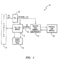
- Fibre Channel controller card 10 includes a PCI-TSI (Peripheral Component Interconnect-Tachyon System Interface) bridge 12, which is connected on one side to the PCI network connector 14.
- PCI-TSI bridge 12 is also connected through a TSI bus 16 to a Tachyon Fibre Channel controller 18.
- the Fibre Channel controller 18 performs the necessary control functions for transferring data between a computer system (e.g., from computer system memory) and a network communications channel (not shown) according to the Fibre Channel Physical and Signalling Interface Specification, Revision 4.3 (June 1994).
- a physical link module 20 for connection to the Fibre Channel communications network, which can be formed of either fiber optics or copper wires.
- a clock generator 22 receives the PCI clock PCICLK and generates an internal clock to the PCI-TSI bridge 12 and the Fibre Channel controller 18.
- a flash ROM 24 can be connected to the PCI-TSI bridge 12 for storing configuration information for the Fibre Channel controller card 10.
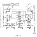
- the PCI-TSI bridge 12 On the PCI side of the PCI-TSI bridge 12, a PCI master 26 and a PCI slave 28 are included to perform the necessary master and slave functions on the PCI bus. PCI address, data and parity information are routed between a PCI interface block 30 and the PCI bus.
- the PCI-TSI bridge 12 also includes write FIFOs 32, a read FIFO 34 and prefetch read FIFOs 32. In the preferred embodiment, six write FIFOs 32 are included, with each write FIFO organized as 32 bits wide and 8 entries deep. The write FIFOs 32 are used to store write data from the Fibre Channel controller 18 destined to computer system memory. By using the write FIFOs 32, a burst data transfer rate of 106 Mbytes per second can be achieved in the preferred embodiment on writes to the PCI bus.
- the bridge 12 also includes two prefetch read FIFOs 36, with each prefetch read FIFO also organized as 32 bits wide and 8 entries deep.
- the read FIFO 34 and prefetch read FIFOs 36 receive data signals ADI ⁇ 31:0> from the PCI interface block 30.
- the Fibre Channel controller 18 can prefetch data from system memory.
- a burst data transfer rate of 88 Mbytes per second can be achieved in the preferred embodiment on reads from the PCI bus.
- the read FIFO 34 is used for non-prefetch reads by the Fibre Channel controller 18.
- a FIFO arbiter 38 determines which of the write FIFOs 32 or read FIFOs 34 or 36 have priority for the PCI master 26. If a TSI-to-PCI cycle is pending in the write FIFOs 32 and the Fibre Channel controller 18 concurrently requests a read cycle on the PCI bus, the FIFO arbiter 38 arbitrates between the concurrent write and read requests. In the preferred embodiment, the write FIFOs 32 are always given the highest priority by the FIFO arbiter 38.
- a TSI master 40 and a TSI slave 40 are included to perform the master and slave functions on the TSI bus.
- the TSI master 40 receives the PCI data signals ADI ⁇ 31:0>. from the PCI interface block 30.
- the TSI master 40 provides data bits TM-TAD ⁇ 31:0> to a TSI interface block 44, which reroutes address, data and parity information to and from the TSI bus 308.
- the TSI interface block 44 also receives data bits TS-TAD ⁇ 31:0> from the TSI slave 42.
- a TSI arbiter 46 is also coupled to PCI slave 28 and TSI master 40, to perform arbitration therefor.
- the Fibre Channel controller 302 transfers data according to the big-endian format.
- a write or read operation between the Fibre Channel controller 18 and the PCI bus involves data, then a big-endian/little endian data format conversion is performed.
- solutions have already been proposed to accomplish such conversion; therefore, it is not discussed further herein.
- required PCI-TSI bridge 12 registers are mapped to memory, with predetermined addresses, where they can be read from and possibly written to as appropriate.
- This register could have configuration byte address offset 04h, for instance, a size of 16 bits, and an access privilege status of PCI configuration read/write.
- Another possible register, present in the exemplary embodiment of the present invention, is a PCI latency timer register which specifies, in terms of PCI clocks, the value of a latency timer of bridge 12 PCI master operations.
- the present invention is concerned with "bridging" devices that differ with respect to one or more of the following: data formatting; speed of handling; and respecting of data continuity.
- data formatting For convenience, the instant invention is being described in terms of its incorporation into an environment that requires all three of those "complication factors" to be handled: that is a PCI-TSI bridging environment.
- the PCI-TSI bridging environment is a particularly good one to consider here because it presents tools (e.g., certain signals) that are conventional enough that the same or similar tools can be identified and used in other environments by those skilled in the art to practice the instant invention therein.
- tools e.g., certain signals
- a PCI bus is a physical interconnect apparatus intended for use between highly integrated peripheral controller components and process/memory systems.
- a PCI bus is intended as a standard interface at the component level in much the same way that ISA, EISA, or Micro Channel buses are standard interfaces at the board level.
- ISA, EISA, and Micro Channel buses provide a common I/O board interface across different platforms and different processor generations, the PCI bus is intended to be a common I/O component interface across different platforms and different processor generations.
- PCI bus The specification for the PCI bus is intended to standardize a local bus on which a large variety of I/O components can directly connect without "glue” logic, i.e., direct component interconnection.
- the PCI bus uses a number of system signals, including the following:
- the PCI specification uses an arbitration approach to bus transactions that is access-based, rather than time-slot-based.
- a master device must arbitrate for each access it performs on the bus.
- a central arbitration scheme is used, wherein each master device has a unique request (REQ) and grant (GNT) signal connected to the central arbiter device.
- REQ unique request
- GNT grant
- a simple request-grant handshake between the arbiter and the master device is used to gain access to the bus.
- a specific arbitration algorithm must be implemented by the arbiter, e.g., priority, rotating priority, fair, etc.
- An arbitration algorithm must be defined to establish a basis for a worst case latency guarantee. The arbitration occurs during a previous access so that no PCI bus cycles are consumed due to the arbitration algorithm.
- the arbiter can implement any scheme as long as only a single GNT is asserted on any clock.
- a device requests the bus by asserting its REQ signal.
- the arbiter determines a device may use the bus, it asserts the device's GNT signal.
- the arbiter may de-assert a device's GNT signal on any clock. Therefore, a device must ensure its GNT is asserted on the clock edge it wants to start a transaction. If the GNT signal is de-asserted, then the transaction must not proceed.
- the GNT signal normally gives a device access to the bus for a single transaction. If the device desires another access, it should continue to assert its REQ signal. A device may de-assert its REQ signal anytime, but the arbiter may interpret this to mean the device no longer requires use of the bus and may de-assert the device's GNT signal.
- the PCI bus may use "arbitration parking," wherein the arbiter asserts the GNT signal to a selected device when no device is currently using or requesting the bus.
- the arbiter can select this default owner any way it wants (e.g., fixed, last used, etc.) or can choose not to park at all, thereby effectively designating itself as the default owner.
- the arbiter asserts a device's GNT signal and the bus is idle, that device must enable its AD and C/BE signal buffers. This requirement insures the arbiter can safely park the bus at some device and know that the bus will not float. If the arbiter does not park the bus, the central resource device in which the arbiter is embedded typically drives the bus, i.e., effectively designating the central resource device as the default owner of the bus.
- the device has lost access to the bus, except in one case.
- the one case is when the arbiter de-asserts the GNT signal coincident with the device asserting the FRAME signal. In this case, the device will continue the transaction. Otherwise, the device must tri-state the AD and C/BE signals. The device must disable all buffers in a single clock to avoid possible contention with the next bus owner.
- the FRAME signal is asserted by being driven to a low voltage by the master device to indicate the beginning of the transaction.
- the first clock edge on which the FRAME signal is asserted is the address phase, and the address and bus command code are transferred by the AD and C/BE signals on that clock edge.
- the next clock edge begins the first of one or more data phases, during which data is transferred by the AD signals between the master device and the target device on each clock edge for which both the IRDY and TRDY signals are asserted by the master device and the target device, respectively. Wait cycles may be inserted in a data phase by either the master device or the target device with the IRDY and TRDY signals.
- the FRAME signal is de-asserted and the IRDY signal is asserted indicating the master device is ready.
- the target device indicates the final data transfer, by asserting the TRDY signal, the PCI bus returns to the idle state with both the FRAME and IRDY signals de-asserted.
- PCI Peripheral Component Interconnect
- TSI is the interface to Hewlett Packard's Tachyon Fibre Channel interface controller.
- Fibre Channel is a multi-topology, physical transport channel that supports both networking and mass storage interconnections. Further information regarding Fibre Channel can be found in the work product of ANSI, Task Group X3T11, at CERN's (Geneva) Fibre Channel standard page on the World Wide Web at http://www.cern.ch/hsi/fcs, and at the Fibre Channel Association's (FCA's) Website at http://www.amdahl.com/ext/carp/fca/fca.htm.
- Tachyon can be found in Hewlett Packard's "Tachyon User's Manual" and at http://tachyon.rose.hp.com/doc.html. To the fullest extent possible, all of the foregoing is incorporated herein by this reference thereto.
- TSI signals include the following:
- the TSI side as the master initiates a request.
- This request is interpreted by the TSI slave 42, and presented to the PCI side through the FIFO 36 and FIFO arbiter 38 blocks.
- the prefetch signal discussed in the immediately preceding section indicates to the prefetch FIFOs whether to wait for subsequent transfers. Assuming that the prefetch signal is asserted, one of the two prefetch FIFOs will enter an appropriate wait state, and the PCI master, upon completion of FIFO arbiter 38 arbitration, will seek ownership of the PCI bus. Once the PCI bus is gained, a first data transfer will be made.
- This data transfer will be of the first 8 D-words (i.e., double-words, where there are 4 bytes each corresponding to a specific address, and where bit 31 is the most significant data bit and bit 0 is the least significant data bit), which is the maximum amount that the TSI can indicate it will accept.
- the PCI - TSI bridge 12 in response to a TSI side request for 8 D-words with prefetch asserted, the PCI - TSI bridge 12 will obtain 16 D-words initially because both prefetch FIFOs 36 are empty. When the first FIFO is empty and the TSI is taking the second 8 D-words, and when prefetch is set again, then the bridge 12 in the exemplary embodiment will get the third 8 D-words. Thus, it should be appreciated that when the prefetch FIFOs 36 are full, PCI wait states are inserted.
- the PCI bus will wait to see if the TSI bus comes back with a second/subsequent address (AD & 32), together with continued assertion of the prefetch signal. If so, the PCI bus will immediately fetch and transfer a second/subsequent block of contiguous data. By this mechanism, the PCI bus can present a steady stream of data to the TSI bus, notwithstanding the fact that the TSI bus cannot easily request such a stream.
- Monitoring of wait counts in the exemplary embodiment is performed by the PCI master. If second and subsequent addresses and prefetch signals continue to be made, the PCI master continues transferring data to the TSI bus.
- the wait count is programmable in the exemplary embodiment. If and when the unit count expires, and the TSI bus does not "come back" as described above, the PCI master can disconnect from the PCI interface, to meet PCI specification requirements.
- a timing diagram showing the waiting and eventual disconnect process is set forth in FIG. 4.
- the present invention simply and efficient streams data in circumstances where data travels at different speeds at the two ends of the transfer, and where continuity of data is desirably, but not easily, maintained.
- the present invention enables efficient use of bandwidth and increased performance characteristics in transfer operations.
- any environment in which a data bridge may be usefully employed can be an environment in which apparatus and methods such as those taught herein may be incorporated.
- a read transfer from a fast bus to a slow bus is described herein, the instant invention may be employed in write transactions also, and/or in transfers from slow to fast buses.
Landscapes
- Engineering & Computer Science (AREA)
- Theoretical Computer Science (AREA)
- General Engineering & Computer Science (AREA)
- Physics & Mathematics (AREA)
- General Physics & Mathematics (AREA)
- Computer Hardware Design (AREA)
- Bus Control (AREA)
Applications Claiming Priority (2)
| Application Number | Priority Date | Filing Date | Title |
|---|---|---|---|
| US692488 | 1996-08-06 | ||
| US08/692,488 US5867675A (en) | 1996-08-06 | 1996-08-06 | Apparatus and method for combining data streams with programmable wait states |
Publications (2)
| Publication Number | Publication Date |
|---|---|
| EP0824238A2 true EP0824238A2 (de) | 1998-02-18 |
| EP0824238A3 EP0824238A3 (de) | 1999-03-24 |
Family
ID=24780787
Family Applications (1)
| Application Number | Title | Priority Date | Filing Date |
|---|---|---|---|
| EP97305892A Withdrawn EP0824238A3 (de) | 1996-08-06 | 1997-08-04 | Vorrichtung und Verfahren zum Kombinieren von Datenströmen mit programmierbaren Wartezuständen |
Country Status (3)
| Country | Link |
|---|---|
| US (1) | US5867675A (de) |
| EP (1) | EP0824238A3 (de) |
| JP (1) | JPH10149334A (de) |
Cited By (1)
| Publication number | Priority date | Publication date | Assignee | Title |
|---|---|---|---|---|
| WO2002037288A3 (en) * | 2000-10-31 | 2002-11-14 | Koninkl Philips Electronics Nv | Extension for the advanced microcontroller bus architecture (amba) |
Families Citing this family (34)
| Publication number | Priority date | Publication date | Assignee | Title |
|---|---|---|---|---|
| US5944808A (en) * | 1997-01-31 | 1999-08-31 | Sun Microsystems, Inc. | Partial parity correction logic |
| US5961640A (en) * | 1997-04-22 | 1999-10-05 | Vlsi Technology, Inc. | Virtual contiguous FIFO having the provision of packet-driven automatic endian conversion |
| US6085271A (en) * | 1998-04-13 | 2000-07-04 | Sandcraft, Inc. | System bus arbitrator for facilitating multiple transactions in a computer system |
| US6425034B1 (en) * | 1998-10-30 | 2002-07-23 | Agilent Technologies, Inc. | Fibre channel controller having both inbound and outbound control units for simultaneously processing both multiple inbound and outbound sequences |
| US7382736B2 (en) | 1999-01-12 | 2008-06-03 | Mcdata Corporation | Method for scoring queued frames for selective transmission through a switch |
| JP3601677B2 (ja) * | 1999-06-09 | 2004-12-15 | 日本電気株式会社 | タスク処理システム |
| US7076586B1 (en) * | 2000-10-06 | 2006-07-11 | Broadcom Corporation | Default bus grant to a bus agent |
| US7356030B2 (en) * | 2000-11-17 | 2008-04-08 | Foundry Networks, Inc. | Network switch cross point |
| US6735218B2 (en) * | 2000-11-17 | 2004-05-11 | Foundry Networks, Inc. | Method and system for encoding wide striped cells |
| US7596139B2 (en) * | 2000-11-17 | 2009-09-29 | Foundry Networks, Inc. | Backplane interface adapter with error control and redundant fabric |
| US7236490B2 (en) * | 2000-11-17 | 2007-06-26 | Foundry Networks, Inc. | Backplane interface adapter |
| US7002980B1 (en) * | 2000-12-19 | 2006-02-21 | Chiaro Networks, Ltd. | System and method for router queue and congestion management |
| US7206283B2 (en) * | 2001-05-15 | 2007-04-17 | Foundry Networks, Inc. | High-performance network switch |
| US7266117B1 (en) | 2002-05-06 | 2007-09-04 | Foundry Networks, Inc. | System architecture for very fast ethernet blade |
| US20120155466A1 (en) * | 2002-05-06 | 2012-06-21 | Ian Edward Davis | Method and apparatus for efficiently processing data packets in a computer network |
| US7468975B1 (en) | 2002-05-06 | 2008-12-23 | Foundry Networks, Inc. | Flexible method for processing data packets in a network routing system for enhanced efficiency and monitoring capability |
| US7649885B1 (en) | 2002-05-06 | 2010-01-19 | Foundry Networks, Inc. | Network routing system for enhanced efficiency and monitoring capability |
| US7187687B1 (en) | 2002-05-06 | 2007-03-06 | Foundry Networks, Inc. | Pipeline method and system for switching packets |
| US20090279558A1 (en) * | 2002-05-06 | 2009-11-12 | Ian Edward Davis | Network routing apparatus for enhanced efficiency and monitoring capability |
| US6901072B1 (en) | 2003-05-15 | 2005-05-31 | Foundry Networks, Inc. | System and method for high speed packet transmission implementing dual transmit and receive pipelines |
| US7817659B2 (en) * | 2004-03-26 | 2010-10-19 | Foundry Networks, Llc | Method and apparatus for aggregating input data streams |
| US8730961B1 (en) | 2004-04-26 | 2014-05-20 | Foundry Networks, Llc | System and method for optimizing router lookup |
| US7657703B1 (en) | 2004-10-29 | 2010-02-02 | Foundry Networks, Inc. | Double density content addressable memory (CAM) lookup scheme |
| US8448162B2 (en) | 2005-12-28 | 2013-05-21 | Foundry Networks, Llc | Hitless software upgrades |
| US20070288690A1 (en) * | 2006-06-13 | 2007-12-13 | Foundry Networks, Inc. | High bandwidth, high capacity look-up table implementation in dynamic random access memory |
| US7903654B2 (en) * | 2006-08-22 | 2011-03-08 | Foundry Networks, Llc | System and method for ECMP load sharing |
| US8238255B2 (en) * | 2006-11-22 | 2012-08-07 | Foundry Networks, Llc | Recovering from failures without impact on data traffic in a shared bus architecture |
| US20090279441A1 (en) | 2007-01-11 | 2009-11-12 | Foundry Networks, Inc. | Techniques for transmitting failure detection protocol packets |
| US8037399B2 (en) * | 2007-07-18 | 2011-10-11 | Foundry Networks, Llc | Techniques for segmented CRC design in high speed networks |
| US8271859B2 (en) * | 2007-07-18 | 2012-09-18 | Foundry Networks Llc | Segmented CRC design in high speed networks |
| US8149839B1 (en) | 2007-09-26 | 2012-04-03 | Foundry Networks, Llc | Selection of trunk ports and paths using rotation |
| US8190881B2 (en) | 2007-10-15 | 2012-05-29 | Foundry Networks Llc | Scalable distributed web-based authentication |
| US8090901B2 (en) | 2009-05-14 | 2012-01-03 | Brocade Communications Systems, Inc. | TCAM management approach that minimize movements |
| US8599850B2 (en) | 2009-09-21 | 2013-12-03 | Brocade Communications Systems, Inc. | Provisioning single or multistage networks using ethernet service instances (ESIs) |
Family Cites Families (10)
| Publication number | Priority date | Publication date | Assignee | Title |
|---|---|---|---|---|
| US5179667A (en) * | 1988-09-14 | 1993-01-12 | Silicon Graphics, Inc. | Synchronized DRAM control apparatus using two different clock rates |
| CA2068010C (en) * | 1991-08-30 | 1996-10-22 | Robert Chih-Tsin Eng | Alternate master bursting data rate management techniques for use in computer systems having dual bus architecture |
| CA2109043A1 (en) * | 1993-01-29 | 1994-07-30 | Charles R. Moore | System and method for transferring data between multiple buses |
| US5613075A (en) * | 1993-11-12 | 1997-03-18 | Intel Corporation | Method and apparatus for providing deterministic read access to main memory in a computer system |
| US5727207A (en) * | 1994-09-07 | 1998-03-10 | Adaptec, Inc. | Method and apparatus for automatically loading configuration data on reset into a host adapter integrated circuit |
| US5557758A (en) * | 1994-11-30 | 1996-09-17 | International Business Machines Corporation | Bridge between two buses of a computer system that determines the location of memory or accesses from bus masters on one of the buses |
| US5740400A (en) * | 1995-06-05 | 1998-04-14 | Advanced Micro Devices Inc. | Reducing cache snooping overhead in a multilevel cache system with multiple bus masters and a shared level two cache by using an inclusion field |
| US5721839A (en) * | 1995-10-13 | 1998-02-24 | Compaq Computer Corporation | Apparatus and method for synchronously providing a fullness indication of a dual ported buffer situated between two asynchronous buses |
| US5734881A (en) * | 1995-12-15 | 1998-03-31 | Cyrix Corporation | Detecting short branches in a prefetch buffer using target location information in a branch target cache |
| US5727218A (en) * | 1996-03-05 | 1998-03-10 | Unisys Corp. | Controlling an apparatus disposed for adapting fiber channel transmissions to an industry standard data bus |
-
1996
- 1996-08-06 US US08/692,488 patent/US5867675A/en not_active Expired - Lifetime
-
1997
- 1997-08-04 EP EP97305892A patent/EP0824238A3/de not_active Withdrawn
- 1997-08-06 JP JP9212109A patent/JPH10149334A/ja active Pending
Cited By (2)
| Publication number | Priority date | Publication date | Assignee | Title |
|---|---|---|---|---|
| WO2002037288A3 (en) * | 2000-10-31 | 2002-11-14 | Koninkl Philips Electronics Nv | Extension for the advanced microcontroller bus architecture (amba) |
| CN100343832C (zh) * | 2000-10-31 | 2007-10-17 | Nxp股份有限公司 | 芯片上系统 |
Also Published As
| Publication number | Publication date |
|---|---|
| US5867675A (en) | 1999-02-02 |
| EP0824238A3 (de) | 1999-03-24 |
| JPH10149334A (ja) | 1998-06-02 |
Similar Documents
| Publication | Publication Date | Title |
|---|---|---|
| US5867675A (en) | Apparatus and method for combining data streams with programmable wait states | |
| US5459839A (en) | System and method for managing queue read and write pointers | |
| US6493776B1 (en) | Scalable on-chip system bus | |
| US6167468A (en) | High-throughput interface between a system memory controller and a peripheral device | |
| US6122690A (en) | On-chip bus architecture that is both processor independent and scalable | |
| KR970000842B1 (ko) | 정보 처리 시스템 및 컴퓨터 시스템 | |
| JP2539614B2 (ja) | ポインタアドレスを発生するための装置および方法 | |
| JP3302357B2 (ja) | Cpuバス制御器 | |
| US6754737B2 (en) | Method and apparatus to allow dynamic variation of ordering enforcement between transactions in a strongly ordered computer interconnect | |
| EP0605170A1 (de) | Rechnersystemschnittstelle | |
| US5379386A (en) | Micro channel interface controller | |
| US5502824A (en) | Peripheral component interconnect "always on" protocol | |
| US6134625A (en) | Method and apparatus for providing arbitration between multiple data streams | |
| US6397279B1 (en) | Smart retry system that reduces wasted bus transactions associated with master retries | |
| US6301632B1 (en) | Direct memory access system and method to bridge PCI bus protocols and hitachi SH4 protocols | |
| US5949981A (en) | Deadlock avoidance in a bridge between a split transaction bus and a single envelope bus | |
| US5388223A (en) | 1-bit token ring arbitration architecture | |
| US20040068603A1 (en) | Reordering of requests between an initiator and the request queue of a bus controller | |
| JPH08263430A (ja) | バス・ターンアラウンド・サイクルを省略する方法及びコンピュータ・システム | |
| EP1222551B1 (de) | Asynchrone zentralisierte multikanal-dma-steuerung | |
| US7096290B2 (en) | On-chip high speed data interface | |
| EP0775960A2 (de) | Busschnittstellen-Logiksystem | |
| US5968144A (en) | System for supporting DMA I/O device using PCI bus and PCI-PCI bridge comprising programmable DMA controller for request arbitration and storing data transfer information | |
| EP1041492A2 (de) | Verfaren und Anordnung zur Optimierung von PCI-Busübertragung | |
| US5418930A (en) | Circuit for interfacing asynchronous to synchronous communications |
Legal Events
| Date | Code | Title | Description |
|---|---|---|---|
| PUAI | Public reference made under article 153(3) epc to a published international application that has entered the european phase |
Free format text: ORIGINAL CODE: 0009012 |
|
| AK | Designated contracting states |
Kind code of ref document: A2 Designated state(s): AT BE CH DE DK ES FI FR GB GR IE IT LI LU MC NL PT SE |
|
| AX | Request for extension of the european patent |
Free format text: AL;LT;LV;RO;SI |
|
| PUAL | Search report despatched |
Free format text: ORIGINAL CODE: 0009013 |
|
| AK | Designated contracting states |
Kind code of ref document: A3 Designated state(s): AT BE CH DE DK ES FI FR GB GR IE IT LI LU MC NL PT SE |
|
| AX | Request for extension of the european patent |
Free format text: AL;LT;LV;RO;SI |
|
| AKX | Designation fees paid | ||
| STAA | Information on the status of an ep patent application or granted ep patent |
Free format text: STATUS: THE APPLICATION IS DEEMED TO BE WITHDRAWN |
|
| 18D | Application deemed to be withdrawn |
Effective date: 19990925 |
|
| REG | Reference to a national code |
Ref country code: DE Ref legal event code: 8566 |