EP0824291A2 - Energiesparender A/D-Wandler - Google Patents
Energiesparender A/D-Wandler Download PDFInfo
- Publication number
- EP0824291A2 EP0824291A2 EP97113793A EP97113793A EP0824291A2 EP 0824291 A2 EP0824291 A2 EP 0824291A2 EP 97113793 A EP97113793 A EP 97113793A EP 97113793 A EP97113793 A EP 97113793A EP 0824291 A2 EP0824291 A2 EP 0824291A2
- Authority
- EP
- European Patent Office
- Prior art keywords
- converter
- signal
- conversion
- conversion system
- standby
- Prior art date
- Legal status (The legal status is an assumption and is not a legal conclusion. Google has not performed a legal analysis and makes no representation as to the accuracy of the status listed.)
- Granted
Links
- 238000006243 chemical reaction Methods 0.000 claims abstract description 59
- 230000004044 response Effects 0.000 claims description 5
- 238000010586 diagram Methods 0.000 description 6
- 230000000694 effects Effects 0.000 description 3
- 238000005070 sampling Methods 0.000 description 3
- 125000004122 cyclic group Chemical group 0.000 description 2
- 230000007423 decrease Effects 0.000 description 2
- 230000004075 alteration Effects 0.000 description 1
- 230000005540 biological transmission Effects 0.000 description 1
- 239000000470 constituent Substances 0.000 description 1
- 230000003247 decreasing effect Effects 0.000 description 1
- 230000004048 modification Effects 0.000 description 1
- 238000012986 modification Methods 0.000 description 1
- 230000000737 periodic effect Effects 0.000 description 1
- 230000005236 sound signal Effects 0.000 description 1
Images


Classifications
-
- H—ELECTRICITY
- H03—ELECTRONIC CIRCUITRY
- H03M—CODING; DECODING; CODE CONVERSION IN GENERAL
- H03M1/00—Analogue/digital conversion; Digital/analogue conversion
- H03M1/002—Provisions or arrangements for saving power, e.g. by allowing a sleep mode, using lower supply voltage for downstream stages, using multiple clock domains or by selectively turning on stages when needed
-
- H—ELECTRICITY
- H03—ELECTRONIC CIRCUITRY
- H03M—CODING; DECODING; CODE CONVERSION IN GENERAL
- H03M1/00—Analogue/digital conversion; Digital/analogue conversion
- H03M1/12—Analogue/digital converters
Definitions
- the present invention relates to a power saving A/D converter and, more particularly, to an A/D converter suited for use in a portable data communication system such as a personal data assistance (PDA).
- PDA personal data assistance
- An A/D converter is used in a portable data communication system for converting an analog input signal, such as an audio signal or image signal, to a digital output signal for data transmission.
- JP-A-3(1991)-185928 proposes an A/D conversion system which repeats A/D conversion in a cyclic operation.
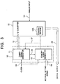
- Fig. 1 shows the proposed A/D conversion system, which comprises an A/D converter 12 for effecting A/D conversion and a control section 36 having therein an interval counter (not shown) for counting the clock pulses in the interval clock input 41.
- the interval counter in the control section 36 counts up to the setting of number of counts specified by the interval setting signal 19
- the interval counter supplies a conversion start signal 38 to the A/D converter 12
- the A/D converter 12 effects A/D conversion of the input analog signal 14, sets the output digital signal 20 after the completion of the conversion and supplies an end of conversion (EOC) signal 40 to the control section 36.
- the control section 36 then supplies a conversion stop signal 39 and activates the interval counter at the same time.
- the interval counter again counts the clock pulses in the interval clock input 41 and supplies a conversion start signal 38 after the count up of the specified setting.
- the present invention provides an A/D conversion system comprising a mode selection section for periodically selecting a conversion mode and a standby mode of the A/D conversion system, an A/D converter for converting an analog input signal to a digital output signal during the conversion mode, and a control section for stopping operation of the A/D converter during the standby mode.
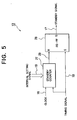
- an A/D conversion system comprises an A/D converter 12 for effecting an A/D conversion of an input analog signal 14, a mode selection section including a timing signal generator 11 for generating timing signals 15 and 18 and a standby signal generator 13 for generating a standby signal 17, and a control section 12A for breaking a current path for the A/D converter 12 in response to the standby signal.
- the A/D converter 12 receives analog input signal 14, converts the same to a digital data in response to a clock signal not shown, and supplies the digital output data 20.
- the timing signal generator 11 receives a clock input 16, and supplies timing signal 15 to the A/D converter 12 for starting and stopping of the A/D conversion and timing signal 18 to the standby signal generator 13 for starting a standby mode.
- the standby signal generator 13 receives an interval setting signal 19, clock input 16 and timing signal 18, and generates standby signal 17, which is supplied to both the A/D converter 12 and the timing generator 11, for effecting a standby mode of the A/D conversion for a duration based on the sampling rate of the A/D conversion.
- standby signal 17 In the standby mode wherein standby signal 17 is active, the current path to the main circuit portion of the A/D converter 12 is cut or broken for power saving by the control section 12A, and the timing signal generator stops for counting of the clock pulses.
- the A/D converter 12 is of a successive approximation type and comprises a resistor string circuit 21 acting as a D/A converter, a comparator 22 for comparison of analog inputs, and a successive approximation register (SAR) 23 for supplying output digital data 20 after completion of the conversion.
- the resistor string circuit 21 receives a digital feed-back data 25 from the successive approximation register 23 and supplies an internal analog data 24 to the comparator 22 based on digital feed-back data 25.
- the comparator 22 compares internal analog data 24 from the resistor string circuit 21 against analog input signal 14 input to the A/D conversion system, to thereby output a result signal 26 assuming a high level or low level based on the result of the comparison.
- the successive approximation register 23 first stores a provisional data, then increases or decreases the provisional data based on the output of the comparator 22, supplies the increased or decreased data as digital feed-back data 25 to the resistor string circuit 21, repeats the increase or decrease of the stored provisional data to the least significant bit, and holds and outputs a final data obtained by the successive approximation.
- Timing signal 15 from the timing signal generator 11 is supplied to the successive approximation register 23, comparator 22 and resistor string circuit 21.
- Standby signal 17 is supplied to the resistor string circuit 21 and comparator 22.
- the standby signal generator 13 comprises a standby counter 27 and a RS-flipflop (RS-FF) 28.
- the standby counter 27 responds to timing signal 18 to start for counting the clock pulses in the clock signal 16, and counts up to the setting by the interval setting signal 19 to output a reset signal 29 for the RS-FF 28.
- the RS-FF 28 is set by timing signal 18 and reset by the output 29 of the standby counter 27, and outputs standby signal 17.
- timing signal 15 including a conversion start signal 15a and a conversion stop signal 15b, as follows.
- conversion start signal 15a turns to an active level or high level
- the comparator 22 shown in Fig. 4 starts for comparing analog input signal 14 against analog internal data 24 decoded by the resistor string circuit 21, to thereby output a high level or low level for allowing the successive approximation register to effect successive approximation.
- conversion stop signal 15b turns to an active level or high level
- the successive approximation register 20 holds the data stored therein as an output digital data 20 for the duration of the next standby mode.
- timing signal 18 turns active to thereby set the RS-FF 28, which outputs an active level of standby signal 17.
- the standby counter 27 starts for counting the clock pulses in clock signal 16 in response to the active level of timing signal 18 and counts up to the setting specified by interval setting signal 19 to thereby output the reset signal for the RS-FF 28, which turns the standby signal 17 to an inactive level.
- the setting specified by the interval setting signal 19 is determined by the sampling period of the A/D conversion system which is a sum of the time length for the A/D conversion and the time length for the standby mode.
- the A/D converter 12 stops its operation. After standby signal 17 is reset by the reset signal 29 from the standby counter 27, the timing signal generator 11 starts for operation to turn conversion start signal 15a to an active level or high level, thereby allowing the A/D converter 12 to effect A/D conversion. In this way, the A/D conversion system operates at a specified sampling rate periodically or intermittently.
- an example of the resistor string circuit 21 in the A/D converter 12 comprises a resistor block or resistor string 30 including a plurality of resistors R 1 to R n connected in series between Vdd line and GND, and a decoder 26 for decoding the voltages at the respective taps p 1 to p n-1 of the resistor string 30.
- a pMOSFET 32 acting as an element of the control section 12A is connected between Vdd line and the resistor string 3.
- the pMOSFET 32 receives standby signal 17 and turns off in response to the active level of standby signal 17 to break the current path for the resistor string 30 for power saving during the standby mode.
- the decoder 31 receives the feed-back data 25 from the successive approximation register 23, and outputs an analog voltage supplied from one of the taps p 1 to p n-1 of the resistor string 30 as a decoded feed-back data.
- the resistor string circuit 21 functions as a D/A converter for decoding the feed-back data 25 from the successive approximation register 26.
- an example of the comparator 22 in the A/D converter of Fig. 4 comprises a pair of differential transistors formed of pMOSFETs MP1 and MP2, a first current mirror formed of nMOSFETs MN1 and MN2 and connected between the pair of differential transistors MP1 and MP2 and GND for acting as active loads for the pair of differential transistors, a second current mirror formed of pMOSFETs MP3 and MP4 and acting as a constant current source for the pair of differential transistors MP1 and MP2, and a constant current source I0 for providing the constant current for pMOSFET MP3 of the second current mirror.
- the common gate of the second current mirror MP3 and MP4 is connected to Vdd line through a switching transistor acting as another element of the control section 12A and formed of pMOSFET MP5 having a gate receiving an inverted signal of standby signal 17.
- the pMOSFET MP1 receives decoded feed-back data 24 or internal analog data whereas the pMOSFET MP2 receives analog input signal 14.
- the comparator 22 compares input analog signal 14 against the decoded feed-back data 24 and outputs a high or low level in accordance with the low or high level of the decoded feed-back data 24 with respect to analog input signal 14.
- the current path for the comparator 22 is cut by the pMOSFET MP5 for power saving.
- the duration for the standby mode can be specified from outside the system to obtain an optimum periodic or intermittent operation of the system while saving the electric power by cutting the current path for the A/D conversion and by stopping the counting operation of the timing generator.
- variable setting for the standby counter 27 enables a single clock signal to control different timings in the system, thereby avoiding an increase of the size of the system. Further, a single clock signal may be used in common for the A/D converter, timing signal generator and the standby signal generator, if desired.
Landscapes
- Engineering & Computer Science (AREA)
- Theoretical Computer Science (AREA)
- Analogue/Digital Conversion (AREA)
Applications Claiming Priority (3)
| Application Number | Priority Date | Filing Date | Title |
|---|---|---|---|
| JP227840/96 | 1996-08-09 | ||
| JP22784096A JP3260631B2 (ja) | 1996-08-09 | 1996-08-09 | 周期的にa/d変換を行うa/dコンバータ回路 |
| JP22784096 | 1996-08-09 |
Publications (3)
| Publication Number | Publication Date |
|---|---|
| EP0824291A2 true EP0824291A2 (de) | 1998-02-18 |
| EP0824291A3 EP0824291A3 (de) | 2001-08-08 |
| EP0824291B1 EP0824291B1 (de) | 2003-01-29 |
Family
ID=16867199
Family Applications (1)
| Application Number | Title | Priority Date | Filing Date |
|---|---|---|---|
| EP97113793A Expired - Lifetime EP0824291B1 (de) | 1996-08-09 | 1997-08-08 | Energiesparender A/D-Wandler |
Country Status (4)
| Country | Link |
|---|---|
| US (1) | US6057795A (de) |
| EP (1) | EP0824291B1 (de) |
| JP (1) | JP3260631B2 (de) |
| DE (1) | DE69718722T2 (de) |
Cited By (1)
| Publication number | Priority date | Publication date | Assignee | Title |
|---|---|---|---|---|
| DE19847662A1 (de) * | 1998-10-15 | 2000-04-20 | Siemens Ag | A/D-Wandler |
Families Citing this family (19)
| Publication number | Priority date | Publication date | Assignee | Title |
|---|---|---|---|---|
| JP2000125213A (ja) * | 1998-10-12 | 2000-04-28 | Fuji Photo Film Co Ltd | 固体撮像装置 |
| US7181635B2 (en) * | 2000-03-13 | 2007-02-20 | Analog Devices, Inc. | Method for placing a device in a selected mode of operation |
| JP4726337B2 (ja) * | 2001-06-27 | 2011-07-20 | ルネサスエレクトロニクス株式会社 | ワンチップマイクロコンピュータ |
| US6642879B2 (en) * | 2001-07-16 | 2003-11-04 | Cirrus Logic, Inc. | Method and system for powering down an analog-to-digital converter into a sleep mode |
| JP4012446B2 (ja) * | 2002-08-23 | 2007-11-21 | 松下電器産業株式会社 | 半導体集積回路 |
| US7071863B1 (en) | 2002-12-06 | 2006-07-04 | Marvell International Ltd. | Low power analog to digital converter having reduced bias during an inactive phase |
| US6839015B1 (en) | 2002-12-06 | 2005-01-04 | Marvell International Ltd. | Low power analog to digital converter |
| GB2439685B (en) | 2005-03-24 | 2010-04-28 | Siport Inc | Low power digital media broadcast receiver with time division |
| US7916711B2 (en) * | 2005-03-24 | 2011-03-29 | Siport, Inc. | Systems and methods for saving power in a digital broadcast receiver |
| US7945233B2 (en) * | 2005-06-16 | 2011-05-17 | Siport, Inc. | Systems and methods for dynamically controlling a tuner |
| US8335484B1 (en) | 2005-07-29 | 2012-12-18 | Siport, Inc. | Systems and methods for dynamically controlling an analog-to-digital converter |
| WO2008047858A1 (en) * | 2006-10-18 | 2008-04-24 | Panasonic Corporation | A/d converter |
| JP4879043B2 (ja) * | 2007-02-22 | 2012-02-15 | 富士通セミコンダクター株式会社 | Ad変換回路及びマイクロコントローラ |
| US7446691B2 (en) * | 2007-03-29 | 2008-11-04 | Symbol Technologies, Inc. | Methods and apparatus for multiplexed signal sources using an analog-to-digital converter |
| US8199769B2 (en) | 2007-05-25 | 2012-06-12 | Siport, Inc. | Timeslot scheduling in digital audio and hybrid audio radio systems |
| US8320823B2 (en) * | 2009-05-04 | 2012-11-27 | Siport, Inc. | Digital radio broadcast transmission using a table of contents |
| US8489053B2 (en) | 2011-01-16 | 2013-07-16 | Siport, Inc. | Compensation of local oscillator phase jitter |
| JP6225240B2 (ja) * | 2016-12-20 | 2017-11-01 | ルネサスエレクトロニクス株式会社 | 集積回路 |
| US20230341348A1 (en) * | 2022-04-21 | 2023-10-26 | Cirrus Logic International Semiconductor Ltd. | Circuitry for electrochemical cells |
Family Cites Families (7)
| Publication number | Priority date | Publication date | Assignee | Title |
|---|---|---|---|---|
| US3610958A (en) * | 1969-05-19 | 1971-10-05 | Bell Telephone Labor Inc | Sample and hold circuit |
| JPH01265722A (ja) * | 1988-04-18 | 1989-10-23 | Nec Corp | アナログ・ディジタル変換器 |
| JPH03185928A (ja) * | 1989-12-14 | 1991-08-13 | Nec Corp | A/dコンバータ回路 |
| US5294928A (en) * | 1992-08-31 | 1994-03-15 | Microchip Technology Incorporated | A/D converter with zero power mode |
| JPH08102675A (ja) * | 1994-09-30 | 1996-04-16 | Matsushita Electric Works Ltd | A/d変換器 |
| US5619204A (en) * | 1995-02-27 | 1997-04-08 | Analog Devices, Incorporated | Analog-to-digital converter with optional low-power mode |
| FR2737066B1 (fr) * | 1995-07-20 | 1997-09-19 | Matra Mhs | Dispositif de conversion analogique-numerique |
-
1996
- 1996-08-09 JP JP22784096A patent/JP3260631B2/ja not_active Expired - Fee Related
-
1997
- 1997-08-08 DE DE69718722T patent/DE69718722T2/de not_active Expired - Fee Related
- 1997-08-08 EP EP97113793A patent/EP0824291B1/de not_active Expired - Lifetime
- 1997-08-11 US US08/907,868 patent/US6057795A/en not_active Expired - Fee Related
Cited By (2)
| Publication number | Priority date | Publication date | Assignee | Title |
|---|---|---|---|---|
| DE19847662A1 (de) * | 1998-10-15 | 2000-04-20 | Siemens Ag | A/D-Wandler |
| US6788235B1 (en) | 1998-10-15 | 2004-09-07 | Infineon Technologies Ag | A/D converter having signaling and requesting capability |
Also Published As
| Publication number | Publication date |
|---|---|
| US6057795A (en) | 2000-05-02 |
| JP3260631B2 (ja) | 2002-02-25 |
| JPH1056383A (ja) | 1998-02-24 |
| DE69718722T2 (de) | 2003-08-21 |
| EP0824291A3 (de) | 2001-08-08 |
| EP0824291B1 (de) | 2003-01-29 |
| DE69718722D1 (de) | 2003-03-06 |
Similar Documents
| Publication | Publication Date | Title |
|---|---|---|
| US6057795A (en) | Power saving A/D converter | |
| US5294928A (en) | A/D converter with zero power mode | |
| US8019316B2 (en) | Lower power wake-up device | |
| US6845454B2 (en) | System and method for selecting between a high and low speed clock in response to a decoded power instruction | |
| JP2000056843A (ja) | 基準電圧生成回路 | |
| US7683730B2 (en) | Differential crystal oscillator circuit with peak regulation | |
| US6642879B2 (en) | Method and system for powering down an analog-to-digital converter into a sleep mode | |
| US20020005710A1 (en) | Frequency sensing NMOS voltage regulator | |
| US7512821B2 (en) | Power supply system and method for supplying power to CPU providing power saving mode | |
| USRE39523E1 (en) | Power control apparatus for a battery-powered communication system | |
| US4737666A (en) | Integrated circuit semiconductor device with reduced power dissipation in a power-down mode | |
| WO1998020609A1 (en) | Low power wake-up system and method | |
| US20250036150A1 (en) | Digital low dropout regulator and electronic device using the same | |
| JPH1131968A (ja) | Ad変換器 | |
| US20100007541A1 (en) | A/d converter | |
| JP2019208141A (ja) | 半導体装置 | |
| WO1999026290A1 (en) | Semiconductor integrated circuit, operating status detector, and electronic equipment | |
| US7391343B2 (en) | Input device | |
| US5087915A (en) | Semiconductor integrated circuit device with analog to digital converter | |
| US20040264288A1 (en) | Timing circuit and method of changing clock period | |
| CN108563278B (zh) | 一种降低参考电压缓冲电路功耗的方法及电路 | |
| JP3098493B2 (ja) | Da変換装置 | |
| JP2695547B2 (ja) | 復帰入力回路 | |
| KR200273011Y1 (ko) | 저전력레벨쉬프터 | |
| US5245342A (en) | Analog to digital converter incorporating summing currents responsive to a digital output thereof |
Legal Events
| Date | Code | Title | Description |
|---|---|---|---|
| PUAI | Public reference made under article 153(3) epc to a published international application that has entered the european phase |
Free format text: ORIGINAL CODE: 0009012 |
|
| AK | Designated contracting states |
Kind code of ref document: A2 Designated state(s): DE GB NL |
|
| AX | Request for extension of the european patent |
Free format text: AL;LT;LV;RO;SI |
|
| PUAL | Search report despatched |
Free format text: ORIGINAL CODE: 0009013 |
|
| AK | Designated contracting states |
Kind code of ref document: A3 Designated state(s): AT BE CH DE DK ES FI FR GB GR IE IT LI LU MC NL PT SE |
|
| AX | Request for extension of the european patent |
Free format text: AL;LT;LV;RO;SI |
|
| 17P | Request for examination filed |
Effective date: 20011105 |
|
| 17Q | First examination report despatched |
Effective date: 20011219 |
|
| AKX | Designation fees paid |
Free format text: DE GB NL |
|
| GRAG | Despatch of communication of intention to grant |
Free format text: ORIGINAL CODE: EPIDOS AGRA |
|
| GRAG | Despatch of communication of intention to grant |
Free format text: ORIGINAL CODE: EPIDOS AGRA |
|
| GRAG | Despatch of communication of intention to grant |
Free format text: ORIGINAL CODE: EPIDOS AGRA |
|
| GRAH | Despatch of communication of intention to grant a patent |
Free format text: ORIGINAL CODE: EPIDOS IGRA |
|
| GRAH | Despatch of communication of intention to grant a patent |
Free format text: ORIGINAL CODE: EPIDOS IGRA |
|
| GRAA | (expected) grant |
Free format text: ORIGINAL CODE: 0009210 |
|
| AK | Designated contracting states |
Designated state(s): DE GB NL |
|
| REG | Reference to a national code |
Ref country code: GB Ref legal event code: FG4D |
|
| REF | Corresponds to: |
Ref document number: 69718722 Country of ref document: DE Date of ref document: 20030306 Kind code of ref document: P |
|
| RAP2 | Party data changed (patent owner data changed or rights of a patent transferred) |
Owner name: NEC ELECTRONICS CORPORATION |
|
| NLT2 | Nl: modifications (of names), taken from the european patent patent bulletin |
Owner name: NEC ELECTRONICS CORPORATION |
|
| PLBE | No opposition filed within time limit |
Free format text: ORIGINAL CODE: 0009261 |
|
| STAA | Information on the status of an ep patent application or granted ep patent |
Free format text: STATUS: NO OPPOSITION FILED WITHIN TIME LIMIT |
|
| 26N | No opposition filed |
Effective date: 20031030 |
|
| PGFP | Annual fee paid to national office [announced via postgrant information from national office to epo] |
Ref country code: DE Payment date: 20070802 Year of fee payment: 11 |
|
| PGFP | Annual fee paid to national office [announced via postgrant information from national office to epo] |
Ref country code: GB Payment date: 20070809 Year of fee payment: 11 |
|
| PGFP | Annual fee paid to national office [announced via postgrant information from national office to epo] |
Ref country code: NL Payment date: 20070815 Year of fee payment: 11 |
|
| GBPC | Gb: european patent ceased through non-payment of renewal fee |
Effective date: 20080808 |
|
| NLV4 | Nl: lapsed or anulled due to non-payment of the annual fee |
Effective date: 20090301 |
|
| PG25 | Lapsed in a contracting state [announced via postgrant information from national office to epo] |
Ref country code: NL Free format text: LAPSE BECAUSE OF NON-PAYMENT OF DUE FEES Effective date: 20090301 |
|
| PG25 | Lapsed in a contracting state [announced via postgrant information from national office to epo] |
Ref country code: DE Free format text: LAPSE BECAUSE OF NON-PAYMENT OF DUE FEES Effective date: 20090303 |
|
| PG25 | Lapsed in a contracting state [announced via postgrant information from national office to epo] |
Ref country code: GB Free format text: LAPSE BECAUSE OF NON-PAYMENT OF DUE FEES Effective date: 20080808 |