EP0825432A2 - Leuchtdiode und optische Vorrichtung - Google Patents
Leuchtdiode und optische Vorrichtung Download PDFInfo
- Publication number
- EP0825432A2 EP0825432A2 EP97114541A EP97114541A EP0825432A2 EP 0825432 A2 EP0825432 A2 EP 0825432A2 EP 97114541 A EP97114541 A EP 97114541A EP 97114541 A EP97114541 A EP 97114541A EP 0825432 A2 EP0825432 A2 EP 0825432A2
- Authority
- EP
- European Patent Office
- Prior art keywords
- light
- sample
- emitting diode
- primary
- reflected
- Prior art date
- Legal status (The legal status is an assumption and is not a legal conclusion. Google has not performed a legal analysis and makes no representation as to the accuracy of the status listed.)
- Withdrawn
Links
Images


Classifications
-
- G—PHYSICS
- G01—MEASURING; TESTING
- G01N—INVESTIGATING OR ANALYSING MATERIALS BY DETERMINING THEIR CHEMICAL OR PHYSICAL PROPERTIES
- G01N21/00—Investigating or analysing materials by the use of optical means, i.e. using sub-millimetre waves, infrared, visible or ultraviolet light
- G01N21/17—Systems in which incident light is modified in accordance with the properties of the material investigated
- G01N21/47—Scattering, i.e. diffuse reflection
- G01N21/4738—Diffuse reflection, e.g. also for testing fluids, fibrous materials
- G01N21/474—Details of optical heads therefor, e.g. using optical fibres
Definitions
- the invention relates to a light emitting diode for use with an optical apparatus. Also, the invention relates to an optical apparatus for determining an optical property of a sample.
- optical apparatus or analyzer which comprises a light source for emitting a light onto a sample to be analyzed, a light detector for receiving the light reflected from (or transmitted through) the sample in order to determine the reflectance (or transmittancy) of the sample.
- a light emitting diode having a PN junction semiconductor has been preferably employed for the light source.
- Fig. 6 illustrates an optical system which has been used for such analyzer.
- the analyzer includes a light source or light emitting diode (LED) 10 for emitting a light Q1.
- the emitted light Q1 is illuminated on a test sample not shown on a plate 11.
- a reflected light Q2 from the sample is detected by an optical sensor 12.
- the sensor 12 transmits a signal having a voltage corresponding to an intensity of the reflected light to obtain the reflectance of the sample on the plate 11.
- a luminous efficiency of LED tends to vary depending upon an environmental temperature and electric current (voltage) to be applied and to decrease in proportion to its service time. Also, the change of luminous efficiency will adversely provide the measured result with error. Therefore, it is important to determine the intensity of light emitted from LED at measurement and, if necessary, the resultant should be corrected based upon the change of light efficiency.
- One method for determining the change of light intensity of the emitted light which is shown in Fig. 6, is to dispose a beam splitter 13 or a half-mirror across the light Q1 so that the light Q1 is divided into a measuring beam Q1' for illumination of the sample and a monitoring beam Q3 for detecting the light intensity of the light Q1 by the use of an optical sensor 14.
- Another method which is shown in Fig. 7, is to dispose an optical sensor 15 beside LED 10 so that a feeble light Q3' emitted laterally from the light source 16 is detected, thereby determining the intensity of the intensity of the light Q1.
- the first method renders the analyzing system more complicated and larger in size because of the additional arrangement of the beam splitter 13 or half mirror between LED 10 and the test sample.
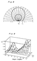
- Fig. 8 is a graph showing a direction dependency of the light intensity of LED.
- a curve G1 illustrates a direction dependency in each direction against the light intensity of light Q1 having the maximum light intensity, in which the intensity of light emitted in the lateral direction spaced at 90 degrees from the upright direction is only about 30% of that of upright direction.
- another curve G2 also illustrates a direction dependency when the light intensity in the upright direction is reduced to 50% by decreasing the voltage (current) applied to LED in which the light intensity of lateral direction is only about 10 %, not 30%, of that of the upright direction in curve G1.
- the light intensity varies with the environmental temperature as well as emitting direction.
- X, Y and Z axes represent an angle of each direction from the upright direction when the upright direction is zero degree, environmental temperature (from 5 to 50 degrees centigrade) and light intensity in each direction, respectively.
- the light intensity in each direction is standardized by that of at 5 degrees centigrade. This shows that the intensity of light changes with the environmental temperature, but the increasing rate in one direction differs from that of another direction. Namely, with the increase of the environmental temperature, the ratio of light intensity of between the monitoring light Q3' and primary light Q1 varies depending upon the emitting angle.
- the direction dependency of the light intensity is caused by a variation of density of the current which flows in the light source, that may be occurred from differences of electric properties of assembled devices, connecting condition of electrodes of the light emitting diode, and the like.
- the light intensity of the primary light Q1 emitted in the normal direction could not be determined precisely by the detection of the monitoring light Q3' emitted laterally, inhibiting the precise measurement of the optical property of the sample.
- a light emitting diode of the invention comprises a body made of resin pervious to light and a light source having a semiconductor mounted in the body for emitting a primary light.
- the body has a surface portion where the primary light emitted from the light source is divided into a first light for an optical analysis and a second light for monitoring an intensity of the primary light.
- the surface portion of the body has small convex and concave portions for dividing the primary light into the first and second lights.
- the surface portion is slanted with respect to the primary light so that the first light is a light which is reflected at the surface portion and the second light is a light which is scattered at the surface portion.
- the surface potion may be a V-shaped recess having first and second surfaces that intersect at a certain angle so that the primary light is divided at an intersection of the first and second surfaces into the first light projected and then reflected on the first surface and the second light projected and then reflected on the second surface.
- An optical apparatus of the invention comprises a light emitting diode.
- the light emitting diode includes a body made of resin which is pervious to light and a light source having a semiconductor mounted in the body for emitting a primary light.
- the body has a surface portion where the primary light emitted from the light source is divided into a first light which is intended to be illuminated on a sample and a second light for monitoring an intensity of the primary light.
- the apparatus further comprises a first detector for detecting the first light from the sample, a second detector for detecting the second light and means for determining an optical property of the sample from outputs of the first and second detectors.
- the light emitting diode and the first and second detectors may be integrally molded in a body of resin.
- the resin of the molded body is impervious to light and the molded body includes a first passage for guiding the first light toward the sample, second passage for guiding a light reflected from the sample toward the first detector and a third passage for guiding the second light toward the second detector.
- the primary light emitted from the light source is divided at the surface portion of the body of the light emitting diode into first and second lights. Subsequently, the first light is reflected at or transmitted through the sample and then detected by the first detector while the second light is detected by the second detector.
- the output of the first detector is used for determining the optical property of the sample.
- the output of the second detector is used for determining the light intensity of the primary light, thereby correcting the resultant optical property. Therefore, the optical property of the sample can be determined with a great precision even when the intensity of the light emitted from the light source has varied due to the changes of voltage or current applied with the light source and/or the environmental temperature.
- an optical analyzer of the invention generally indicated reference numeral 100 includes a printed circuit board 101 having an electric circuit (not shown) on both or either side thereof.
- a light emitting diode (LED) generally indicated by reference numeral 102 has a base 103, body 104 made of resin (e.g., epoxy resin) pervious to light, PN junction semiconductor 105 integrally molded in the body 104 and capable of emitting light when it is applied with voltage and a pair of terminals 106 electrically communicating the semiconductor 105 with the circuit on the printed board 101.
- the semiconductor 105 is so directed that a primary light L having the maximum light intensity is emitted vertical to and away from base 103.
- the body 104 generally in the form of solid cylinder is secured at its one end to the base 103.
- the other end of body 104 remote from the base 103 is formed with a surface 107 which is slanted at about 45 degrees against the longitudinal axis of the body 104.
- the body 104 is formed at its peripheral portion adjacent the slanted surface 107 with a domed surface portion or convex lens 108, thereby most part of the primary light L emitted from the semiconductor 105 is reflected at the slanted surface 107 and then transmitted substantially along a central axis of the convex lens 108 toward a sample 109 (e.g., urine, blood, or chemical compound) retained on a sample retaining plate 110 (e.g., PET (polyethylene terephthalate) plate) to be releasably disposed above the circuit board 101.
- a sample 109 e.g., urine, blood, or chemical compound
- a sample retaining plate 110 e.g., PET (polyethylene terephthalate) plate
- the body 104 is typically formed by molding and therefore undoubtedly the slanted surface 107 has small or microscopic convex and concave portions therein rather than perfect mirror, thereby the primary light L emitted from the semiconductor 105 in part scatters out of the slanted surface 107.
- LED 102 thus constructed is so arranged that the reflected primary light L1 travels in a direction away from the circuit board 101 toward the sample 109.
- a first optical sensor 111 having a pair of terminals 112 is disposed above LED 102 so that it can detect a part of light L1' of the primary light L which would be reflected at the sample 109.
- the first optical sensor 111 is so oriented that it can receive the reflected light L1' traveling in a direction which intersects with the primary light L1 advancing to the sample 109 at an angle of 45 degrees.
- a second optical sensor 113 having a pair of terminals 114 is disposed to oppose the slanted surface 107 of LED 102 so that it can detect the scattered light L2 at the slanted surface 107.
- the optical sensors 111 and 113 are commercially available under the trade designation PIN photodiode (SPS-503A1) from SANYO ELECTRIC CO., Ltd. Also, the terminals 112 and 114 are secured on the printed circuit board 101 and electrically communicated with the circuit on the board 101.
- LED 102 and optical sensors 111 and 113 are integrally molded in a molded body 115 on the circuit board 101 with a resin, such as ABS, which is impervious to light.
- the molded body 115 includes therein a first passage 116 which extends from the convex lens 108 to one or top surface 117 facing the sample retaining plate 110 and a second passage 118 which extends from the first optical sensor 111 to the top surface 117 so that the primary light L1 from the semiconductor 105 can travel through the first passage 116 to illuminate the sample 109 on the sample retaining plate 110 and then the reflected light L1' travels to the first optical sensor 111.
- the molded body 115 also includes a third passage 119 which extends from the slanted surface 107 to the second optical sensor 113 so that the scattered light L2 of the primary light can reach the second optical sensor 113.
- the passages 117, 118 and 119 are formed in the molded body 115 by arranging tubes corresponding to respective passages in a mold prior to the molding of body 115.
- openings of the first and second passages 116 and 118, confronting the sample 109, are covered with a transparent plate not shown to prevent foreign matters from entering into the passages 116 and 118.
- a thermal sensor 120 is integrally mounted in the molded body 115 for detecting a temperature.
- the thermal sensor 120 includes a pair of terminals 121 which is electrically connected with the circuit on the board 101. It is to be understood that the thermal sensor 120 may be disposed outside the molded body 115.
- CPU central processing unit
- a reference plate (not shown) which retains thereon a reference sample having a known reflectance of, for example, 50% is so positioned that the reference sample confronts the openings of the passages 116 and 118.
- CPU 122 instructs LED 102 to energize the semiconductor 105 for emitting.
- the primary light L emitted from the semiconductor 105 travels toward the slanted surface 107 where the major part thereof reflects.
- the reflected primary light L1 further travels through the convex lens 108 and the passage 116 to reach the sample 109 on the sample retaining plate 110 where it reflects again.
- Part of the second reflected primary light L1' travels into the passage 118 to the first optical sensor 111 which detects the intensity of second reflected primary light L1'.
- the optical sensor 111 outputs a signal corresponding to the detected light intensity to CPU 122.
- the primary light L from the semiconductor 105 scatters at the slanted surface 107 due to the existence of the microscopic convex and concave portions.
- the scattered light L2 travels through the passage 119 to reach the second optical sensor 113.
- the optical sensor 113 outputs a signal corresponding to the intensity of the detected scattered light L2 to CPU 122.
- the thermal sensor 120 outputs a signal corresponding to the temperature of the molded body 115 to CPU 122.
- the reference plate has a reflectance R REF of 50% and output voltages V REF (1) and V REF (2) of the first and second optical sensors 111 and 113 are 44 milli-volts and of 4.2 milli-volts, respectively.
- outputs voltages V SAM (1) and V SAM (2)of the first and second optical sensors 111 and 113 are 12 milli-volts and 4.2 milli-volts.
- LED 130 may have a conventional configuration.
- the body 131 of LED 130 is formed at its distal end away from the base 132 with a domed surface 133.
- a central portion 134 of the domed surface 133 is formed with small or microscopic convex and concave portions by a suitable manner such as sandblast.
- the convex and concave portions may be formed at molding of the body 131 by providing corresponding convex and concave portions on an inner surface of the mold.
- the molded surface includes microscopic convex and concave potions. Therefore, it is not necessary to form such small convex and concave portions by the above described techniques. In this event, a feeble scattering light is generated when the primary light transmits the surface of the LED body. Therefore, by detecting the feeble scattering light by the optical sensor, the light intensity of the primary light can be corrected.
- Fig. 4 shows another embodiment of the invention.
- the body 141 of LED 140 has a V-shaped recess 142 with its bottom portion confronting the semiconductor 143.
- two surfaces 144 and 145 of the V-shaped recess 142 are spaced apart from each other at 90 degrees.
- the primary light emitted from the semiconductor 143 is illuminated at the bottom portion of the V-shaped recess 142 where it is divided into two, one light L1 reflected at the surface 144 and then being transmitted in one direction for illumination of test sample and the other light reflected at the surface 145 and then transmitted in the opposite direction for monitoring.
- Fig. 5 shows still another embodiment of the LED body 151 in which the domed surface or convex lens is eliminated therefrom.
- optical analyzer is designed to determine the reflectance of the sample, it may be modified to determine a transmittancy of light.
Landscapes
- Physics & Mathematics (AREA)
- Health & Medical Sciences (AREA)
- Life Sciences & Earth Sciences (AREA)
- Chemical & Material Sciences (AREA)
- Analytical Chemistry (AREA)
- Biochemistry (AREA)
- General Health & Medical Sciences (AREA)
- General Physics & Mathematics (AREA)
- Immunology (AREA)
- Pathology (AREA)
- Investigating Or Analysing Materials By Optical Means (AREA)
- Led Device Packages (AREA)
- Led Devices (AREA)
Applications Claiming Priority (2)
| Application Number | Priority Date | Filing Date | Title |
|---|---|---|---|
| JP222194/96 | 1996-08-23 | ||
| JP8222194A JPH1065218A (ja) | 1996-08-23 | 1996-08-23 | 光学系用led |
Publications (2)
| Publication Number | Publication Date |
|---|---|
| EP0825432A2 true EP0825432A2 (de) | 1998-02-25 |
| EP0825432A3 EP0825432A3 (de) | 1998-04-08 |
Family
ID=16778629
Family Applications (1)
| Application Number | Title | Priority Date | Filing Date |
|---|---|---|---|
| EP97114541A Withdrawn EP0825432A3 (de) | 1996-08-23 | 1997-08-22 | Leuchtdiode und optische Vorrichtung |
Country Status (3)
| Country | Link |
|---|---|
| US (1) | US5910663A (de) |
| EP (1) | EP0825432A3 (de) |
| JP (1) | JPH1065218A (de) |
Cited By (2)
| Publication number | Priority date | Publication date | Assignee | Title |
|---|---|---|---|---|
| FR2777731A1 (fr) * | 1998-04-17 | 1999-10-22 | Christian Pierre Marie Estival | Diode electroluminescente a faisceau annulaire lateral par effet de reflexion interne |
| WO2009153609A1 (en) * | 2008-06-20 | 2009-12-23 | 77 Elektronika Mϋszeripari Kft. | Optical measuring unit and method for carrying out a reflective measurement |
Families Citing this family (3)
| Publication number | Priority date | Publication date | Assignee | Title |
|---|---|---|---|---|
| EP3006910A4 (de) * | 2013-05-29 | 2017-02-08 | Konica Minolta, Inc. | Beleuchtungsvorrichtung und vorrichtung zur messung von beleuchtungseigenschaften |
| CN107683109B (zh) * | 2015-06-25 | 2021-06-08 | 费森尤斯医疗控股股份有限公司 | 直接光差分测量系统 |
| DE102020000968A1 (de) * | 2020-02-14 | 2021-08-19 | Giesecke+Devrient Currency Technology Gmbh | Optischer Sensor zur Prüfung von Wertdokumenten |
Family Cites Families (5)
| Publication number | Priority date | Publication date | Assignee | Title |
|---|---|---|---|---|
| JPS61219186A (ja) * | 1985-03-25 | 1986-09-29 | Toshiba Corp | 発光装置 |
| FR2581768B1 (fr) * | 1985-05-10 | 1987-09-04 | Thomson Csf | Composant optoelectrique bidirectionnel formant coupleur optique |
| EP0472963A3 (en) * | 1990-08-27 | 1992-07-08 | Sumitomo Electric Industries, Limited | Light emitting diode for photosensor and photosensor using such light emitting diode |
| JP3242476B2 (ja) * | 1992-06-29 | 2001-12-25 | 沖電気工業株式会社 | 光半導体装置 |
| JPH06309685A (ja) * | 1993-04-26 | 1994-11-04 | Nippon Conlux Co Ltd | 光学式情報記録再生装置のレーザ出力制御装置 |
-
1996
- 1996-08-23 JP JP8222194A patent/JPH1065218A/ja active Pending
-
1997
- 1997-08-21 US US08/916,174 patent/US5910663A/en not_active Expired - Fee Related
- 1997-08-22 EP EP97114541A patent/EP0825432A3/de not_active Withdrawn
Cited By (3)
| Publication number | Priority date | Publication date | Assignee | Title |
|---|---|---|---|---|
| FR2777731A1 (fr) * | 1998-04-17 | 1999-10-22 | Christian Pierre Marie Estival | Diode electroluminescente a faisceau annulaire lateral par effet de reflexion interne |
| WO2009153609A1 (en) * | 2008-06-20 | 2009-12-23 | 77 Elektronika Mϋszeripari Kft. | Optical measuring unit and method for carrying out a reflective measurement |
| EA020255B1 (ru) * | 2008-06-20 | 2014-09-30 | 77 Электроника Мусерипари Кфт. | Оптическое измерительное устройство и способ проведения отражательных измерений |
Also Published As
| Publication number | Publication date |
|---|---|
| JPH1065218A (ja) | 1998-03-06 |
| EP0825432A3 (de) | 1998-04-08 |
| US5910663A (en) | 1999-06-08 |
Similar Documents
| Publication | Publication Date | Title |
|---|---|---|
| US5701181A (en) | Fiber optic diffuse light reflectance sensor utilized in the detection of occult blood | |
| US5518689A (en) | Diffused light reflectance readhead | |
| JP3868516B2 (ja) | 光度計のマルチ検出器読取りヘッド | |
| US7142299B2 (en) | Turbidity sensor | |
| US4683579A (en) | Method and apparatus for measuring blood constituent counts | |
| US4755058A (en) | Device and method for measuring light diffusely reflected from a nonuniform specimen | |
| US4859864A (en) | Sensor and method for detecting the presence of air bubbles in liquid | |
| AU685711B2 (en) | Diffused light reflectance readhead | |
| CA1226453A (en) | Device and method for measuring light diffusely reflected from a nonuniform specimen | |
| EP3465166B1 (de) | Optische vorrichtung | |
| CA2457170A1 (en) | Multiwavelength readhead for use in the determination of analytes in body fluids | |
| WO2003039363A1 (en) | Instrument for measuring biological information and method for measuring biological information | |
| EP2300804B1 (de) | Optische messeinheit und verfahren zur durchführung einer reflexionsmessung | |
| US5910663A (en) | Optical system and light emitting diode having a light dividing surface portion | |
| AU2002310007B2 (en) | Optical turbidimeter with a lens tube | |
| EP0185285A2 (de) | Messapparat für Flüssigkeitspegel | |
| EP0903571A2 (de) | Vorrichtung und Verfahren zur Bestimmung der Konzentration spezifischer Substanzen | |
| DE50001263D1 (de) | Optische Messanordnung zur Bestimmung der Transmissions- und Streustrahlung | |
| US6084662A (en) | Light transmittance measuring device and process for separating transmittance and reflectance | |
| JPH07508587A (ja) | 光学的測定装置 | |
| WO2021102175A1 (en) | Methods and compositions for lateral flow analyte assays | |
| JPH05196566A (ja) | 流体検出装置および気液界面検出装置 | |
| RU2180957C2 (ru) | Устройство для исследования взвесей эритроцитов, лейкоцитов и тромбоцитов | |
| EP0762110A1 (de) | Reflexionslesekopf für diffuses Licht | |
| US20260126384A1 (en) | Device and method for measuring turbidity |
Legal Events
| Date | Code | Title | Description |
|---|---|---|---|
| PUAI | Public reference made under article 153(3) epc to a published international application that has entered the european phase |
Free format text: ORIGINAL CODE: 0009012 |
|
| PUAL | Search report despatched |
Free format text: ORIGINAL CODE: 0009013 |
|
| AK | Designated contracting states |
Kind code of ref document: A2 Designated state(s): DE FR GB IT |
|
| AX | Request for extension of the european patent |
Free format text: AL;LT;LV;RO;SI |
|
| AK | Designated contracting states |
Kind code of ref document: A3 Designated state(s): AT BE CH DE DK ES FI FR GB GR IE IT LI LU MC NL PT SE |
|
| AX | Request for extension of the european patent |
Free format text: AL;LT;LV;RO;SI |
|
| 17P | Request for examination filed |
Effective date: 19981005 |
|
| AKX | Designation fees paid |
Free format text: DE FR GB IT |
|
| RBV | Designated contracting states (corrected) |
Designated state(s): DE FR GB IT |
|
| STAA | Information on the status of an ep patent application or granted ep patent |
Free format text: STATUS: THE APPLICATION IS DEEMED TO BE WITHDRAWN |
|
| 18D | Application deemed to be withdrawn |
Effective date: 20020301 |