EP0825765B1 - Circuit de correction de données de capteur d'images - Google Patents
Circuit de correction de données de capteur d'images Download PDFInfo
- Publication number
- EP0825765B1 EP0825765B1 EP97305039A EP97305039A EP0825765B1 EP 0825765 B1 EP0825765 B1 EP 0825765B1 EP 97305039 A EP97305039 A EP 97305039A EP 97305039 A EP97305039 A EP 97305039A EP 0825765 B1 EP0825765 B1 EP 0825765B1
- Authority
- EP
- European Patent Office
- Prior art keywords
- radiation
- sensors
- image
- detector
- value
- Prior art date
- Legal status (The legal status is an assumption and is not a legal conclusion. Google has not performed a legal analysis and makes no representation as to the accuracy of the status listed.)
- Expired - Lifetime
Links
- 238000012937 correction Methods 0.000 title description 2
- 230000002093 peripheral effect Effects 0.000 claims description 50
- 230000005855 radiation Effects 0.000 claims description 41
- 238000000034 method Methods 0.000 claims description 32
- 238000005070 sampling Methods 0.000 claims description 30
- 230000000873 masking effect Effects 0.000 claims description 4
- 238000012546 transfer Methods 0.000 description 12
- 230000003287 optical effect Effects 0.000 description 10
- 239000000872 buffer Substances 0.000 description 8
- 238000005286 illumination Methods 0.000 description 7
- 238000003491 array Methods 0.000 description 3
- 230000000694 effects Effects 0.000 description 3
- 238000003384 imaging method Methods 0.000 description 3
- 230000004075 alteration Effects 0.000 description 2
- 238000004458 analytical method Methods 0.000 description 2
- 238000010586 diagram Methods 0.000 description 2
- 238000002474 experimental method Methods 0.000 description 2
- 238000013459 approach Methods 0.000 description 1
- 230000015556 catabolic process Effects 0.000 description 1
- 238000006243 chemical reaction Methods 0.000 description 1
- 238000006731 degradation reaction Methods 0.000 description 1
- 230000001419 dependent effect Effects 0.000 description 1
- 230000010354 integration Effects 0.000 description 1
- 238000002955 isolation Methods 0.000 description 1
- 238000004519 manufacturing process Methods 0.000 description 1
- 238000013178 mathematical model Methods 0.000 description 1
- 230000007935 neutral effect Effects 0.000 description 1
- 238000012634 optical imaging Methods 0.000 description 1
- 238000012360 testing method Methods 0.000 description 1
Images

Classifications
-
- H—ELECTRICITY
- H04—ELECTRIC COMMUNICATION TECHNIQUE
- H04N—PICTORIAL COMMUNICATION, e.g. TELEVISION
- H04N25/00—Circuitry of solid-state image sensors [SSIS]; Control thereof
- H04N25/70—SSIS architectures; Circuits associated therewith
- H04N25/701—Line sensors
-
- H—ELECTRICITY
- H04—ELECTRIC COMMUNICATION TECHNIQUE
- H04N—PICTORIAL COMMUNICATION, e.g. TELEVISION
- H04N25/00—Circuitry of solid-state image sensors [SSIS]; Control thereof
- H04N25/70—SSIS architectures; Circuits associated therewith
- H04N25/71—Charge-coupled device [CCD] sensors; Charge-transfer registers specially adapted for CCD sensors
Definitions
- the present invention relates to a method and apparatus for input scanning an image using a detector comprising an array of radiation sensors, such as a CCD array.
- CCD arrays are used in a variety of fields to monitor incident radiation, particularly light.
- the radiation sensitive devices integrate the incident radiation to develop a charge relating to the total radiation incident on the device which, in a transfer step, is transferred into the associated transfer buffers.
- the transfer buffers are constituted by one or more shift registers. The contents of the shift register or shift registers are then shifted out to obtain information relating to the incident radiation. For optimum speed, while the array is being exposed, the contents of the shift register or registers from the preceding transfer are simultaneously shifted out.
- CCD arrays have a particular application in the field of image scanning such as flat bed scanning.
- a transparency is positioned between a source of illumination and a linear CCD array, relative movement being caused between the array and the transparency so that the transparency containing the image is scanned.
- aberrations are apparent particularly when scanning transparencies with high contrasts. This is manifested in a continuously variable level shift which appears to depend on the degree of illumination.
- a DC offset value is then obtained from an isolation buffer (which is a transfer buffer not associated with a corresponding radiation sensitive device).
- a further known method of reducing peripheral response is to mount and accurately align a slit close to the pixel array to shield peripheral areas of the CCD array (in particular the transfer buffers) from the incident illumination.
- US-A-4974810 describes a method of compensating for flare light in an optical imaging system in which a flare light detector views flare light and produces a signal related to the amount of light viewed.
- a compensator reduces the signal from the image detector in response to the signal from the flare light detector. This system cannot compensate accurately for peripheral response.
- US-A-5280354 describes a video camera with a flare correcting circuit.
- the flare correcting circuit detects the average luminance level during a time period of eight fields of the digital video signal. This system cannot accurately correct for peripheral response in an image signal which may change significantly between consecutive image fields.
- a method of input scanning an image using a linear CCD array detector comprising an array of radiation sensors comprising
- the first aspect of the present invention provides an improved method of correcting for peripheral response in an input scanning system in which a detector and an image are moved relative to each other in a scanning operation.
- a single data value is obtained from each radiation sensor during each sampling period, and the peripheral response value for each sampling period is determined independently of the peripheral response values for the other sampling periods.
- the first aspect of the present invention provides a particularly useful method of compensation of the spurious detector response known generally as peripheral response.
- Peripheral response results in an error in each pixel value. It has been found that the amount of peripheral response is proportional to the total radiation incident on the detector over a given sampling period.
- peripheral response in a CCD is a charge which builds up in transfer buffers associated with the radiation sensors in response to incident radiation. It has been found that this "peripheral response" is proportional to the total illumination on the CCD array for any given scan line. The fact that the unwanted peripheral response is directly proportional to the amount of light incident on the CCD array indicates that this may also be a capacitive effect between two parts of the CCD. For a given capacitance, the resulting voltage will be directly proportional to the collected charge which is proportional to the total incident light.
- the peripheral response value may be obtained using hardware or software.
- the peripheral response value may be obtained by inputting the sum of the data values into a suitably programmed look-up table.
- the peripheral response value may be obtained in software by performing a predetermined algorithm on the sum of the data values.
- the predetermined algorithm or the programming of the look-up table may be determined by developing a suitable mathematical model of the peripheral response. Preferably however they are determined in a previous calibration procedure which characterises the peripheral response of the detector to varying amounts of incident light.
- the calibration procedure comprises the following steps:
- the "defining" step e) may comprise fitting a curve to a number of data points obtained in a number of repeats of step c).
- the "defining” step e) may simply comprise storing the values obtained in step c) and loading the values (or related values) into a look-up table.
- S (a(x+c)) - S b
- S is the peripheral response value
- S b is a black level signal representative of the pixel data values when no light is incident on the detector
- a and c are constants for a given length of sampling period
- x is proportional to the number of sensors not masked in the respective step b) or d) of the calibration procedure.
- the algorithm may vary (either in terms of the form of the equation or the values of the constants) depending on the particular detector being used.
- the value x is proportional to the total radiation incident on the exposed part of the array (since the illumination is uniform across the array). Therefore a suitably normalised version of the total radiation value can be input as the value x in the above algorithm.
- the summed value (suitably normalised) is inserted as the value x in the above equation, and the constants S b , a and c are determined in the previous calibration procedure.
- the offset value S can then be obtained by the following equation: Where is the sum of all signals S i on pixel i, summed over all CCD pixels.
- the value of the constants a and c will depend on the particular CCD array used, the sampling period and the colour of the incident radiation.
- apparatus for input scanning an image comprising
- the apparatus may be implemented in hardware or software.
- the means for determining a peripheral response value may comprise a look-up table which provides the peripheral response value on input of the value obtained by the first means.
- the radiation may comprise white light or coloured light (for instance alternating red, green and blue light).
- peripheral CCD response Two sources of image degradation are peripheral CCD response, and optical flare.
- the following description of an embodiment of the invention first presents results which characterise and separate the peripheral response and optical flare responses of the Fairchild 191 CCD array. It is first shown that there is a DC offset in the observed signal from the CCD and that this is due to a peripheral CCD response and not optical flare. This response is characterised and plotted as a function of the illuminated area of the CCD array. A method of correcting this offset according to the present invention is then presented.
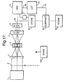
- Figure 17 illustrates an example of input scanning apparatus according to the second aspect of the present invention.
- the apparatus can be used in input scanning, and also in the following experimental and calibration procedures.
- the image scanning apparatus comprises a source of white light 1, and a rotating filter disc 2. Light passes through the filter disc 2 and appropriately illuminates a transparency 3. The illuminated transparency 3 is imaged onto a linear CCD array 5 by an imaging lens 4.
- the filter disc 2 may comprise three sectors arranged to transmit red, blue and green light successively.
- the transparency 4 (containing the image) is mounted in a conventional holder (not shown) and moved by a drive 100. Light from the transparency 4 impinges on a linear CCD array 5.
- the filter disc 2 may comprise three sectors arranged to transmit red, blue, and green light successively.
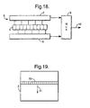
- FIG 18 is a schematic view of the CCD 5 shown in Figure 17 arranged in a line.
- the CCD array 5 comprises a plurality of photodiodes 6. In practice, there may be at least 6000 photodiodes 6 but only ten are shown in Figure 18.
- Two shift registers 7,8 are positioned on either side of the photodiodes 6 and alternate photodiodes are electrically connected to the shift registers 7,8 respectively.
- the serial outputs of the shift registers 7,8 are connected to a multiplexer 9 which provides a multiplexed output 10 corresponding to the previous contents of the photodiodes in sequence.
- An example of a suitable CCD array 5 is the Fairchild CCD 151 or CCD 191.
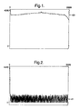
- FIG. 1 the vertical (y) axis represents the base 10 logarithm of the CCD signal response from each pixel in the CCD array and the horizontal (x) axis represents distance along the CCD array.
- the light source 1 is set up to give a reasonably uniform response across the 6000 pixels of the CCD array 5 as shown in the graph of Figure 1.
- This graph shows the level 20 of illumination with the lens aperture set at F/4 and the transparency 3 removed.
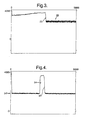
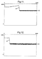
- Figure 2 shows the black level 21 obtained when the lens 4 is covered. A screen is then placed in the plane of the transparency 3 covering approximately half the illuminated area, see Figure 3.
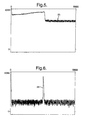
- FIG. 4 shows the edge 23 of the first screen, and the edge 24 of the second screen.
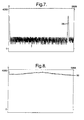
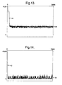
- the black level 24' in this Figure can be compared with that of Figures 2 and 3. This shows how the unwanted response is dependent upon the amount of light incident on the CCD array and a similar method is used later to characterise the effect. It is still not possible to establish from these results the cause of the unwanted response since both optical flare and spurious CCD response are likely to be dependant on the size of illuminated area.
- the unwanted peripheral response is related to the illuminated length of the CCD or, equivalently, to the total amount of light on the CCD. This can be expressed as follows: Where S is the unwanted peripheral response signal (in linear space), S i is the signal on pixel i, and the summation is carried out over all CCD pixels.
- Figure 17 is a plan view of the transparency 3 shown in Figure 17.
- a strip of imaged pixels are schematically indicated at 50.
- the scanning elements 1, 2, 4 and 5 are driven with respect to the transparency 3 by a scan drive indicated schematically at 100.
- the transparency 3 moves with respect to 1, 2, 4 and 5 which is equivalent to the imaged pixels 50 traversing the transparency as indicated at 51.
- light from the pixels 50 in the positions shown in Figure 19 irradiates the CCD 5.
- the radiation sensors 6 on the CCD integrate the incident radiation during the sampling period to develop a charge relating to the total radiation incident on each respective sensor which, in a transfer step, is transferred into the associated transfer buffers 7,8.
- the transfer buffers 7,8 are constituted by one or more shift registers.
- the contents of the shift registers 7,8 are then shifted out to multiplexer 9.
- the multiplexer 9 provides a multiplexed output 10 corresponding to the previous contents of the photodiodes 6 in sequence.
- the pixel value data values 10 are input to adder 11 and store 12 during a sample period under control of clock 17.
- Adder 11 sums the pixel data values over the sampling period and inputs the resulting sum into look-up table 13.
- the look-up table 13 is programmed previously (as discussed below) and outputs a DC offset value 14 representative of the peripheral response of the CCD array 5 during the present sampling period.
- the stored pixel data values are then readout from store 12 and the offset value 14 is subtracted from each pixel data value by subtracter 15.
- the resulting corrected pixel data values are then stored in data store 16.
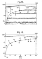
- a curve of the form illustrated in Figure 16 is calculated.
- the x coordinates are then converted from distance in mm to total incident radiation during the sampling period (by a linear conversion) and the resulting curve is then programmed into the look-up table in terms of a set of pairs of values, each pair comprising one value for the input sum 18 and one value for the output peripheral response value 14.
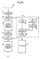
- Charge is integrated in the photodiodes 6 during a sampling period as indicated at 60.
- the charge is then transferred and readout as indicated at 61 and 62.
- the readout pixel data values are then processed during the next sampling period as indicated at 70.
- the pixel data values are first stored at 63 and summed at 64.
- the summed value 18 is then converted into a peripheral response value by performing a predetermined algorithm at 65.
- the resulting peripheral response value 14 is then subtracted from each pixel data value stored at 63 and the resulting modified pixel values are stored at 67. The process is then repeated for the next sampling period 60.
Landscapes
- Engineering & Computer Science (AREA)
- Multimedia (AREA)
- Signal Processing (AREA)
- Transforming Light Signals Into Electric Signals (AREA)
- Facsimile Scanning Arrangements (AREA)
- Solid State Image Pick-Up Elements (AREA)
- Facsimile Image Signal Circuits (AREA)
Claims (9)
- Procédé de balayage de capture d'une image en utilisant un détecteur à réseau linéaire de CCD comprenant un réseau de senseurs de rayonnement, le procédé comprenant les étapes consistant à1) exposer les senseurs de rayonnement au rayonnement de l'image;2) produire un mouvement relatif entre le détecteur et l'image, de sorte que le détecteur reçoive le rayonnement de parties successives de l'image sur plusieurs périodes d'échantillonnage,
et, pour chaque période respective d'échantillonnage:3) obtenir une valeur de donnée de chaque senseur de rayonnement;4) sommer les valeurs de données obtenues durant la période d'échantillonnage;5) déterminer une valeur de la réponse périphérique en fonction de la somme obtenue à l'étape 4); et6) modifier les valeurs de données en fonction de la valeur de la réponse périphérique obtenue à l'étape 5). - Procédé selon la revendication 1, dans lequel une valeur de donnée unique est obtenue de chaque senseur de rayonnement durant chaque période d'échantillonnage, et la valeur de la réponse périphérique pour chaque période d'échantillonnage est déterminée indépendamment des valeurs des réponses périphériques pour les autres périodes d'échantillonnage.
- Procédé selon l'une quelconque des revendications précédentes, dans lequel la valeur de la réponse périphérique est obtenue d'une table de recherche en entrant la somme des valeurs de données dans la table de recherche.
- Procédé selon l'une quelconque des revendications précédentes, dans lequel la valeur de la réponse périphérique est obtenue selon un algorithme prédéterminé.
- Procédé selon la revendication 4, dans lequel l'algorithme prédéterminé comprend
Sb est un signal de niveau du noir, représentatif de la valeur de donnée du pixel lorsqu'aucune lumière n'atteint le détecteur,
a et c sont des constantes pour une longueur donnée de la période d'échantillonnage, et
x est la somme des valeurs de données. - Procédé selon l'une quelconque des revendications précédentes, comprenant en outre la détermination de l'algorithme prédéterminé ou la programmation de la table de recherche dans une procédure d'étalonnage.
- Procédé selon la revendication 6, dans lequel la procédure d'échantillonnage comprend les étapes consistant àa) éclairer le détecteur pour donner une réponse essentiellement uniforme sur le réseau de senseurs;b) masquer une partie du réseau de senseurs de sorte qu'un certain nombre de senseurs soient occultés;c) obtenir un signal du noir des senseurs occultés;d) masquer un nombre différent de senseurs et répéter l'étape c); ete) définir la variation du signal du noir avec le nombre de senseurs occultés.
- Procédé selon l'une quelconque des revendications précédentes, dans lequel les valeurs de données sont modifiées en soustrayant la valeur de la réponse périphérique de la valeur de donnée de chaque pixel.
- Appareil de balayage de capture d'un image, l'appareil comprenant1) un détecteur à réseau linéaire de CCD comprenant un réseau de senseurs de rayonnement;2) un imageur pour exposer les senseurs de rayonnement au rayonnement de l'image;3) un entraínement pour produire un mouvement relatif entre le détecteur et l'image, par lequel le détecteur reçoit le rayonnement de parties successives de l'image sur plusieurs périodes d'échantillonnage;4) des moyens pour obtenir une valeur de donnée de chaque senseur de rayonnement pour chaque période d'échantillonnage;5) des moyens pour sommer les valeurs de données obtenues pour chaque période d'échantillonnage;6) des moyens pour déterminer une valeur de la réponse périphérique conformément à la somme; et7) des moyens pour modifier les valeurs de données conformément à la valeur de la réponse périphérique.
Applications Claiming Priority (2)
| Application Number | Priority Date | Filing Date | Title |
|---|---|---|---|
| GB9616859 | 1996-08-12 | ||
| GBGB9616859.6A GB9616859D0 (en) | 1996-08-12 | 1996-08-12 | Improvements in input scanning an image |
Publications (2)
| Publication Number | Publication Date |
|---|---|
| EP0825765A1 EP0825765A1 (fr) | 1998-02-25 |
| EP0825765B1 true EP0825765B1 (fr) | 2002-09-18 |
Family
ID=10798340
Family Applications (1)
| Application Number | Title | Priority Date | Filing Date |
|---|---|---|---|
| EP97305039A Expired - Lifetime EP0825765B1 (fr) | 1996-08-12 | 1997-07-09 | Circuit de correction de données de capteur d'images |
Country Status (5)
| Country | Link |
|---|---|
| US (1) | US5995247A (fr) |
| EP (1) | EP0825765B1 (fr) |
| JP (1) | JP3889123B2 (fr) |
| DE (1) | DE69715542T2 (fr) |
| GB (1) | GB9616859D0 (fr) |
Families Citing this family (2)
| Publication number | Priority date | Publication date | Assignee | Title |
|---|---|---|---|---|
| US6650445B1 (en) * | 1999-09-17 | 2003-11-18 | Hewlett-Packard Development Company, L.P. | Optical scanner providing compensation for non-uniform bulb illumination |
| US8008908B2 (en) * | 2007-06-25 | 2011-08-30 | Allegro Microsystems, Inc. | Low power magnetic field sensor |
Family Cites Families (8)
| Publication number | Priority date | Publication date | Assignee | Title |
|---|---|---|---|---|
| JPS6113888A (ja) * | 1984-06-29 | 1986-01-22 | Hitachi Denshi Ltd | テレビジヨンカメラ装置における実時間フレア調整方法 |
| GB8506050D0 (en) * | 1985-03-08 | 1985-04-11 | Crosfield Electronics Ltd | Operating ccd arrays |
| GB8606200D0 (en) * | 1986-03-13 | 1986-04-16 | Crosfield Electronics Ltd | Operating radiation sensors |
| US4974810A (en) * | 1989-12-18 | 1990-12-04 | Eastman Kodak Company | Flare light compensation |
| US5280354A (en) * | 1991-04-04 | 1994-01-18 | Sony Corporation | Video camera with flare correcting circuit |
| US5223841A (en) * | 1992-06-29 | 1993-06-29 | The United States Of America As Represented By The Secretary Of The Navy | Calibration method and apparatus for collecting the output of an array of detector cells |
| JPH07225434A (ja) * | 1994-02-14 | 1995-08-22 | Fuji Photo Film Co Ltd | 画像読取装置 |
| US5471244A (en) * | 1994-05-31 | 1995-11-28 | 3M Company | Automatic dark level zeroing for an analog video signal |
-
1996
- 1996-08-12 GB GBGB9616859.6A patent/GB9616859D0/en active Pending
-
1997
- 1997-07-09 EP EP97305039A patent/EP0825765B1/fr not_active Expired - Lifetime
- 1997-07-09 DE DE69715542T patent/DE69715542T2/de not_active Expired - Fee Related
- 1997-07-31 US US08/904,271 patent/US5995247A/en not_active Expired - Fee Related
- 1997-08-07 JP JP21303997A patent/JP3889123B2/ja not_active Expired - Fee Related
Also Published As
| Publication number | Publication date |
|---|---|
| JPH1093861A (ja) | 1998-04-10 |
| DE69715542T2 (de) | 2003-01-16 |
| DE69715542D1 (de) | 2002-10-24 |
| US5995247A (en) | 1999-11-30 |
| EP0825765A1 (fr) | 1998-02-25 |
| JP3889123B2 (ja) | 2007-03-07 |
| GB9616859D0 (en) | 1996-09-25 |
Similar Documents
| Publication | Publication Date | Title |
|---|---|---|
| US6330081B1 (en) | Crosstalk cancellation in a multi-color CCD signal processor | |
| US7355159B2 (en) | Image scanner and method for detecting a defect in an image to be scanned | |
| CN102577355B (zh) | 预测图像采集系统的缺陷的方法及其相关系统 | |
| US5122871A (en) | Method of color separation scanning | |
| JPH051449B2 (fr) | ||
| JP2002303548A (ja) | 平坦な測定対象物の光電測定用装置 | |
| US6295383B1 (en) | Intensity correction in an optical scanner | |
| US4051458A (en) | Video amplitude related measurements in image analysis | |
| EP0605402B1 (fr) | Balayage en couleurs séparées de l'image d'entrée et insertion d'une image dans la mise en page | |
| US20020100863A1 (en) | Optical image scanner with color and intensity compensation during lamp warmup | |
| US5995247A (en) | Input scanning an image | |
| JP2718510B2 (ja) | 着色周期性パターンの検査方法 | |
| US4698515A (en) | Method of operating radiation sensors | |
| EP0703702B1 (fr) | Appareil de lecture d'image et méthode pour leur mise en oeuvre | |
| WO2001088512A1 (fr) | Detection et correction de defauts issus des references d'etalonnage de scanner | |
| US5592309A (en) | Multiple lens separation scanner | |
| Mumzhiu | CCD camera as a tool for color measurement | |
| US5157516A (en) | Method of incorporating a scanned image into a page layout | |
| US5111308A (en) | Method of incorporating a scanned image into a page layout | |
| JP4735534B2 (ja) | 画像処理装置、画像読取装置およびプログラム | |
| JPH04170853A (ja) | 画像読取装置 | |
| JP2662100B2 (ja) | 光電変換素子の位置検出方法 | |
| JPH0865450A (ja) | 画像読み取り装置及び画像読み取り方法及び撮像装置 | |
| JPH05110881A (ja) | カラー読取装置 | |
| GB2404519A (en) | Image scanner with lamp intensity compensation during warm-up |
Legal Events
| Date | Code | Title | Description |
|---|---|---|---|
| PUAI | Public reference made under article 153(3) epc to a published international application that has entered the european phase |
Free format text: ORIGINAL CODE: 0009012 |
|
| AK | Designated contracting states |
Kind code of ref document: A1 Designated state(s): DE GB |
|
| 17P | Request for examination filed |
Effective date: 19980813 |
|
| AKX | Designation fees paid |
Free format text: DE GB |
|
| RBV | Designated contracting states (corrected) |
Designated state(s): DE GB |
|
| 17Q | First examination report despatched |
Effective date: 20010719 |
|
| GRAG | Despatch of communication of intention to grant |
Free format text: ORIGINAL CODE: EPIDOS AGRA |
|
| GRAG | Despatch of communication of intention to grant |
Free format text: ORIGINAL CODE: EPIDOS AGRA |
|
| GRAH | Despatch of communication of intention to grant a patent |
Free format text: ORIGINAL CODE: EPIDOS IGRA |
|
| GRAH | Despatch of communication of intention to grant a patent |
Free format text: ORIGINAL CODE: EPIDOS IGRA |
|
| GRAA | (expected) grant |
Free format text: ORIGINAL CODE: 0009210 |
|
| AK | Designated contracting states |
Kind code of ref document: B1 Designated state(s): DE GB |
|
| REG | Reference to a national code |
Ref country code: GB Ref legal event code: FG4D |
|
| REF | Corresponds to: |
Ref document number: 69715542 Country of ref document: DE Date of ref document: 20021024 |
|
| PLBE | No opposition filed within time limit |
Free format text: ORIGINAL CODE: 0009261 |
|
| STAA | Information on the status of an ep patent application or granted ep patent |
Free format text: STATUS: NO OPPOSITION FILED WITHIN TIME LIMIT |
|
| 26N | No opposition filed |
Effective date: 20030619 |
|
| PGFP | Annual fee paid to national office [announced via postgrant information from national office to epo] |
Ref country code: GB Payment date: 20050706 Year of fee payment: 9 |
|
| PGFP | Annual fee paid to national office [announced via postgrant information from national office to epo] |
Ref country code: DE Payment date: 20050707 Year of fee payment: 9 |
|
| PG25 | Lapsed in a contracting state [announced via postgrant information from national office to epo] |
Ref country code: GB Free format text: LAPSE BECAUSE OF NON-PAYMENT OF DUE FEES Effective date: 20060709 |
|
| PG25 | Lapsed in a contracting state [announced via postgrant information from national office to epo] |
Ref country code: DE Free format text: LAPSE BECAUSE OF NON-PAYMENT OF DUE FEES Effective date: 20070201 |
|
| GBPC | Gb: european patent ceased through non-payment of renewal fee |
Effective date: 20060709 |