EP0826164B1 - Composant optique pour la production d'un rayonnement laser pulse - Google Patents
Composant optique pour la production d'un rayonnement laser pulse Download PDFInfo
- Publication number
- EP0826164B1 EP0826164B1 EP96913414A EP96913414A EP0826164B1 EP 0826164 B1 EP0826164 B1 EP 0826164B1 EP 96913414 A EP96913414 A EP 96913414A EP 96913414 A EP96913414 A EP 96913414A EP 0826164 B1 EP0826164 B1 EP 0826164B1
- Authority
- EP
- European Patent Office
- Prior art keywords
- coating
- ensemble
- layer
- laser
- layers
- Prior art date
- Legal status (The legal status is an assumption and is not a legal conclusion. Google has not performed a legal analysis and makes no representation as to the accuracy of the status listed.)
- Revoked
Links
- 230000005855 radiation Effects 0.000 title claims description 39
- 230000003287 optical effect Effects 0.000 title claims description 34
- 238000000576 coating method Methods 0.000 claims description 100
- 239000011248 coating agent Substances 0.000 claims description 95
- JBRZTFJDHDCESZ-UHFFFAOYSA-N AsGa Chemical compound [As]#[Ga] JBRZTFJDHDCESZ-UHFFFAOYSA-N 0.000 claims description 30
- 229910001218 Gallium arsenide Inorganic materials 0.000 claims description 29
- 239000000463 material Substances 0.000 claims description 29
- 239000004065 semiconductor Substances 0.000 claims description 19
- 238000000034 method Methods 0.000 claims description 16
- 238000010521 absorption reaction Methods 0.000 claims description 13
- MDPILPRLPQYEEN-UHFFFAOYSA-N aluminium arsenide Chemical compound [As]#[Al] MDPILPRLPQYEEN-UHFFFAOYSA-N 0.000 claims description 12
- 230000008569 process Effects 0.000 claims description 12
- 239000006185 dispersion Substances 0.000 claims description 11
- 239000000758 substrate Substances 0.000 claims description 11
- 229910052782 aluminium Inorganic materials 0.000 claims description 10
- XAGFODPZIPBFFR-UHFFFAOYSA-N aluminium Chemical compound [Al] XAGFODPZIPBFFR-UHFFFAOYSA-N 0.000 claims description 9
- 229910052733 gallium Inorganic materials 0.000 claims description 8
- 229910052785 arsenic Inorganic materials 0.000 claims description 7
- 238000004519 manufacturing process Methods 0.000 claims description 7
- 230000008859 change Effects 0.000 claims description 5
- 229910052751 metal Inorganic materials 0.000 claims description 5
- 239000002184 metal Substances 0.000 claims description 5
- GYHNNYVSQQEPJS-UHFFFAOYSA-N Gallium Chemical compound [Ga] GYHNNYVSQQEPJS-UHFFFAOYSA-N 0.000 claims description 4
- 229910000530 Gallium indium arsenide Inorganic materials 0.000 claims description 4
- 239000011358 absorbing material Substances 0.000 claims description 4
- RQNWIZPPADIBDY-UHFFFAOYSA-N arsenic atom Chemical compound [As] RQNWIZPPADIBDY-UHFFFAOYSA-N 0.000 claims description 4
- 230000000694 effects Effects 0.000 claims description 4
- KRHYYFGTRYWZRS-UHFFFAOYSA-M Fluoride anion Chemical compound [F-] KRHYYFGTRYWZRS-UHFFFAOYSA-M 0.000 claims description 3
- 239000004411 aluminium Substances 0.000 claims 4
- 150000001875 compounds Chemical class 0.000 claims 2
- 230000003667 anti-reflective effect Effects 0.000 claims 1
- 239000010410 layer Substances 0.000 description 141
- 239000006096 absorbing agent Substances 0.000 description 33
- 239000013078 crystal Substances 0.000 description 15
- 230000002745 absorbent Effects 0.000 description 10
- 239000002250 absorbent Substances 0.000 description 10
- 229910016036 BaF 2 Inorganic materials 0.000 description 7
- 229910004261 CaF 2 Inorganic materials 0.000 description 6
- 229910000980 Aluminium gallium arsenide Inorganic materials 0.000 description 5
- 230000008878 coupling Effects 0.000 description 5
- 238000010168 coupling process Methods 0.000 description 5
- 238000005859 coupling reaction Methods 0.000 description 5
- QGZKDVFQNNGYKY-UHFFFAOYSA-N Ammonia Chemical compound N QGZKDVFQNNGYKY-UHFFFAOYSA-N 0.000 description 4
- MHAJPDPJQMAIIY-UHFFFAOYSA-N Hydrogen peroxide Chemical compound OO MHAJPDPJQMAIIY-UHFFFAOYSA-N 0.000 description 4
- BQCADISMDOOEFD-UHFFFAOYSA-N Silver Chemical compound [Ag] BQCADISMDOOEFD-UHFFFAOYSA-N 0.000 description 4
- 239000011651 chromium Substances 0.000 description 4
- 238000005530 etching Methods 0.000 description 4
- 229910052709 silver Inorganic materials 0.000 description 4
- 239000004332 silver Substances 0.000 description 4
- 150000002222 fluorine compounds Chemical class 0.000 description 3
- VYZAMTAEIAYCRO-UHFFFAOYSA-N Chromium Chemical compound [Cr] VYZAMTAEIAYCRO-UHFFFAOYSA-N 0.000 description 2
- KRHYYFGTRYWZRS-UHFFFAOYSA-N Fluorane Chemical compound F KRHYYFGTRYWZRS-UHFFFAOYSA-N 0.000 description 2
- IEPNMLJMIRCTIV-UHFFFAOYSA-H aluminum;lithium;strontium;hexafluoride Chemical compound [Li+].[F-].[F-].[F-].[F-].[F-].[F-].[Al+3].[Sr+2] IEPNMLJMIRCTIV-UHFFFAOYSA-H 0.000 description 2
- 229910021529 ammonia Inorganic materials 0.000 description 2
- 239000006117 anti-reflective coating Substances 0.000 description 2
- 230000008901 benefit Effects 0.000 description 2
- BJQHLKABXJIVAM-UHFFFAOYSA-N bis(2-ethylhexyl) phthalate Chemical compound CCCCC(CC)COC(=O)C1=CC=CC=C1C(=O)OCC(CC)CCCC BJQHLKABXJIVAM-UHFFFAOYSA-N 0.000 description 2
- 229910052804 chromium Inorganic materials 0.000 description 2
- 238000010276 construction Methods 0.000 description 2
- 238000003384 imaging method Methods 0.000 description 2
- 238000005086 pumping Methods 0.000 description 2
- 230000006798 recombination Effects 0.000 description 2
- 238000005215 recombination Methods 0.000 description 2
- 241001101998 Galium Species 0.000 description 1
- OAICVXFJPJFONN-UHFFFAOYSA-N Phosphorus Chemical compound [P] OAICVXFJPJFONN-UHFFFAOYSA-N 0.000 description 1
- 229910004298 SiO 2 Inorganic materials 0.000 description 1
- XUIMIQQOPSSXEZ-UHFFFAOYSA-N Silicon Chemical compound [Si] XUIMIQQOPSSXEZ-UHFFFAOYSA-N 0.000 description 1
- 229910010413 TiO 2 Inorganic materials 0.000 description 1
- 230000006978 adaptation Effects 0.000 description 1
- FTWRSWRBSVXQPI-UHFFFAOYSA-N alumanylidynearsane;gallanylidynearsane Chemical compound [As]#[Al].[As]#[Ga] FTWRSWRBSVXQPI-UHFFFAOYSA-N 0.000 description 1
- 230000015572 biosynthetic process Effects 0.000 description 1
- 239000002800 charge carrier Substances 0.000 description 1
- 238000001816 cooling Methods 0.000 description 1
- 230000007423 decrease Effects 0.000 description 1
- 230000001419 dependent effect Effects 0.000 description 1
- 239000000975 dye Substances 0.000 description 1
- 230000005684 electric field Effects 0.000 description 1
- 229920006332 epoxy adhesive Polymers 0.000 description 1
- PCHJSUWPFVWCPO-UHFFFAOYSA-N gold Chemical compound [Au] PCHJSUWPFVWCPO-UHFFFAOYSA-N 0.000 description 1
- 229910052737 gold Inorganic materials 0.000 description 1
- 239000010931 gold Substances 0.000 description 1
- 230000017525 heat dissipation Effects 0.000 description 1
- 229910052738 indium Inorganic materials 0.000 description 1
- APFVFJFRJDLVQX-UHFFFAOYSA-N indium atom Chemical compound [In] APFVFJFRJDLVQX-UHFFFAOYSA-N 0.000 description 1
- 239000000203 mixture Substances 0.000 description 1
- 230000005693 optoelectronics Effects 0.000 description 1
- 230000035515 penetration Effects 0.000 description 1
- 230000035699 permeability Effects 0.000 description 1
- 229910052698 phosphorus Inorganic materials 0.000 description 1
- 239000011574 phosphorus Substances 0.000 description 1
- 239000011241 protective layer Substances 0.000 description 1
- 229910052710 silicon Inorganic materials 0.000 description 1
- 239000010703 silicon Substances 0.000 description 1
- 239000002356 single layer Substances 0.000 description 1
- 239000007787 solid Substances 0.000 description 1
- 229910052712 strontium Inorganic materials 0.000 description 1
- 230000009466 transformation Effects 0.000 description 1
- 230000007704 transition Effects 0.000 description 1
- 238000011144 upstream manufacturing Methods 0.000 description 1
Images


Classifications
-
- H—ELECTRICITY
- H01—ELECTRIC ELEMENTS
- H01S—DEVICES USING THE PROCESS OF LIGHT AMPLIFICATION BY STIMULATED EMISSION OF RADIATION [LASER] TO AMPLIFY OR GENERATE LIGHT; DEVICES USING STIMULATED EMISSION OF ELECTROMAGNETIC RADIATION IN WAVE RANGES OTHER THAN OPTICAL
- H01S3/00—Lasers, i.e. devices using stimulated emission of electromagnetic radiation in the infrared, visible or ultraviolet wave range
- H01S3/10—Controlling the intensity, frequency, phase, polarisation or direction of the emitted radiation, e.g. switching, gating, modulating or demodulating
- H01S3/11—Mode locking; Q-switching; Other giant-pulse techniques, e.g. cavity dumping
- H01S3/1106—Mode locking
- H01S3/1112—Passive mode locking
- H01S3/1115—Passive mode locking using intracavity saturable absorbers
- H01S3/1118—Semiconductor saturable absorbers, e.g. semiconductor saturable absorber mirrors [SESAMs]; Solid-state saturable absorbers, e.g. carbon nanotube [CNT] based
-
- G—PHYSICS
- G02—OPTICS
- G02F—OPTICAL DEVICES OR ARRANGEMENTS FOR THE CONTROL OF LIGHT BY MODIFICATION OF THE OPTICAL PROPERTIES OF THE MEDIA OF THE ELEMENTS INVOLVED THEREIN; NON-LINEAR OPTICS; FREQUENCY-CHANGING OF LIGHT; OPTICAL LOGIC ELEMENTS; OPTICAL ANALOGUE/DIGITAL CONVERTERS
- G02F1/00—Devices or arrangements for the control of the intensity, colour, phase, polarisation or direction of light arriving from an independent light source, e.g. switching, gating or modulating; Non-linear optics
- G02F1/35—Non-linear optics
- G02F1/3523—Non-linear absorption changing by light, e.g. bleaching
-
- H—ELECTRICITY
- H01—ELECTRIC ELEMENTS
- H01S—DEVICES USING THE PROCESS OF LIGHT AMPLIFICATION BY STIMULATED EMISSION OF RADIATION [LASER] TO AMPLIFY OR GENERATE LIGHT; DEVICES USING STIMULATED EMISSION OF ELECTROMAGNETIC RADIATION IN WAVE RANGES OTHER THAN OPTICAL
- H01S3/00—Lasers, i.e. devices using stimulated emission of electromagnetic radiation in the infrared, visible or ultraviolet wave range
- H01S3/05—Construction or shape of optical resonators; Accommodation of active medium therein; Shape of active medium
- H01S3/06—Construction or shape of active medium
- H01S3/0602—Crystal lasers or glass lasers
- H01S3/0604—Crystal lasers or glass lasers in the form of a plate or disc
-
- H—ELECTRICITY
- H01—ELECTRIC ELEMENTS
- H01S—DEVICES USING THE PROCESS OF LIGHT AMPLIFICATION BY STIMULATED EMISSION OF RADIATION [LASER] TO AMPLIFY OR GENERATE LIGHT; DEVICES USING STIMULATED EMISSION OF ELECTROMAGNETIC RADIATION IN WAVE RANGES OTHER THAN OPTICAL
- H01S3/00—Lasers, i.e. devices using stimulated emission of electromagnetic radiation in the infrared, visible or ultraviolet wave range
- H01S3/05—Construction or shape of optical resonators; Accommodation of active medium therein; Shape of active medium
- H01S3/06—Construction or shape of active medium
- H01S3/0627—Construction or shape of active medium the resonator being monolithic, e.g. microlaser
-
- H—ELECTRICITY
- H01—ELECTRIC ELEMENTS
- H01S—DEVICES USING THE PROCESS OF LIGHT AMPLIFICATION BY STIMULATED EMISSION OF RADIATION [LASER] TO AMPLIFY OR GENERATE LIGHT; DEVICES USING STIMULATED EMISSION OF ELECTROMAGNETIC RADIATION IN WAVE RANGES OTHER THAN OPTICAL
- H01S3/00—Lasers, i.e. devices using stimulated emission of electromagnetic radiation in the infrared, visible or ultraviolet wave range
- H01S3/10—Controlling the intensity, frequency, phase, polarisation or direction of the emitted radiation, e.g. switching, gating, modulating or demodulating
- H01S3/11—Mode locking; Q-switching; Other giant-pulse techniques, e.g. cavity dumping
- H01S3/1123—Q-switching
- H01S3/113—Q-switching using intracavity saturable absorbers
Definitions
- the invention relates to a method for producing an optical component with a predetermined Reflection factor for laser radiation, preferably usable for generation short laser pulses in a laser resonator according to claim 1 and a laser for generating short pulses according to claim 7.
- Short pulses in the micro to femtosecond range can be achieved through mode coupling and Q-switching or generate mode-locked Q-switching within a laser resonator, what can be done with a saturable absorber introduced into the laser resonator.
- saturable absorbers dyes or semiconductors are used, their absorption capacity decreases with increasing radiation intensity. In this way a coupling takes place the different resonator modes to short pulses oscillating in the resonator, e.g. in a vivid way in H. Weber / G. Herziger, Laser - Basics and Applications, Physik Verlag GmbH, Weinheim / Bergstr. 1972, p. 144 ff.
- Saturable absorbers could now, as in U. Keller, "revolution in the generation of ultra-short Pulse ", TR Transfer No. 23, 1994, pp. 22-24, e.g. as a so-called” Antiresonant Fabry-Perot Saturable Absorber "are formed.
- a semiconductor absorber was used which was placed in an approximately 400 ⁇ m thick Fabry-Perot interferometer was integrated with sandwich construction. This sandwich structure was analogous to a Fabry-Perot (etalon) two mirror elements. The space between the two Mirror elements were filled with the saturable absorbing semiconductor material.
- Another sandwich-like structure of a saturable absorber is from L.R. Brovelli et al., "Self-starting soliton modelocked Ti-sapphire laser using a thin saturable absorber, electronics Letters, Vol. 31, No. 4, 1995, pp. 287-288. With the “sandwich absorber” described here (see right column p. 287, second uppermost paragraph) only one of the both Fabry-Perot levels through an anti-reflective coating, i.e. an anti-reflection fee replaced.
- the saturable absorbent material is here between the two Sandwich cover elements.
- a coating ensemble is used a number of layers is generated, whereby here only a removal or a change a single shift can change the entire shift behavior.
- there is a matrix-like coupling of the whole Layers with each other e.g. from the theoretical explanations in M. Born and E. Wolf, Principles of Optics, Pergamon Press, 1975, pp. 55-70.
- the change the physical data of a layer affects the properties of the overall layer.
- the optical can now in the invention Components through the appropriate determination of the coating ensemble properties given as they are now needed for an optimal resonator.
- the optical layer thicknesses and / or the layer material and the Places in the ensemble are targeted, desired and therefore optimal adjustable.
- optical properties can be taken into account; it can also i.a. Requirements for the layer resistance, the exact frequency-based course of reflection and in particular, as also explained below, the optimal location of the absorber material and thus its optimal effect can be selected.
- this coating can not only less expensive, but by using larger tolerances in the used optical layer thicknesses and their refractive index are produced.
- the excellent "design freedom" which offers a variety of possible combinations, has been advantageous in the layer structure and its materials.
- the laser according to the invention is used to generate short pulses, particularly in the micro to Femtosecond range and has at least one optical component, manufactured according to the above method according to the invention in the laser resonator.
- On the component surface is an optical coating ensemble according to the invention with first and second optical layers and at least one third semiconductor material layer. Neighbors first and second layers have a different optical refractive index and every third layer is a saturable absorbing material for the wavelength of the Laser radiation.
- the first, second and third layers are thus phase-locked together Way arranged by their arrangement and their layer thicknesses that the component has a predetermined reflection factor for the radiation when it is incident.
- the third Layer is in one place or the third layers are in places in the ensemble, where a predetermined normalized intensity when the radiation hits the Component results.
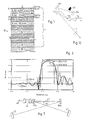
- FIG. 1 shows a section through the layer structure of a coating ensemble 1 , which acts as a reflector and at the same time as a saturable absorber. Since, for example, a semiconductor, namely gallium arsenide, is used as the saturable absorbent material, semiconductor materials related to the structure of the structure have also been used for the remaining layers in order to ensure perfect growth during the coating process (low-temperature MBE-grown at approx. 400 ° C ) to obtain.
- a semiconductor namely gallium arsenide
- the layer containing the saturable absorber is preferably allowed to grow at lower temperatures, ie between 200 ° C. and 600 ° C.
- the recombination times of the charge carriers generated by the laser pulse can be influenced and are then adjustable between a few 100 fs and a few nanoseconds. This recombination time is adapted to the required properties of the laser, such as. B.
- the coating ensemble 1 has a 5 nm thick gallium arsenide layer top layer 4 (GaAs), then a 40 nm thick aluminum arsenide layer 5 (AlAs), a 20 nm thick gallium arsenide layer 6 (GaAs) as a saturable absorbent Material, a 70 nm thick aluminum arsenide layer 7 , a 10 nm thick gallium arsenide layer 9 and then preferably 25 double layers consisting of a 59.4 nm thick aluminum-doped gallium arsenide layer 11 (Al 15% Ga 85% As) and a 69.2 nm thick aluminum arsenide layer 13.
- the entire coating ensemble 1 is applied to a gallium arsenide substrate 15.
- the wave resistance of a layer Z x is the wave resistance Z 0 of the empty space (approximately that of air) divided by the refractive index (square root of the relative dielectric constant at a relative magnetic permeability of 1, which is usually given here).
- the wave resistance Z 0 of the empty space is approximately 376.7 ⁇ .
- the course of reflection of the coating ensemble 1 described above is shown in FIG .
- the idea is now to compensate the wavelength dependency based on the structure of the coating ensemble 1 with the absorption given by the absorbing material for a predetermined wavelength range. This can be achieved by choosing the correct location of the absorber layer 6 .
- the reflection factor of the ensemble 1 for a position of the absorber layer 6 is shown shifted outwards by 20 nm (roughly dashed) and once inwards (finely dashed) by 20 nm compared to the position shown in FIG. 1.
- the solid line is shown the wavelength of the center frequency of 830 nm with which the mode-locked laser works.
- the intensity curve parallel to the surface normal in the coating becomes analog from the electric field strength to the reflection factor described above, where also here the phase relationships of the reflections of the partial waves of the respective inner interfaces superimposed in phases need to be such.
- the course of the intensity within the coating ensemble 1 shown in FIG. 1 for three different wavelengths in free space of 830 nm, 840 nm and 850 nm is shown in FIG. 4 .
- the wavelength specifications always refer to that in free space.
- the arrangement has a coating ensemble 19 which is arranged on a heat sink 17 and acts as a laser resonator mirror with a saturable absorber, which, according to the coating ensemble 1 described above, has a maximum reflection at 840 nm and acts as an approximately 100% mirror with a 1 - 2% saturable absorber.
- the other resonator mirror 20 which acts as an outcoupling mirror, has a reflection of 98% and has an expert coating, which will not be discussed further here.
- a Cr LiSAF crystal 23 [chromium-doped lithium strontium aluminum fluoride crystal LiSrAlF 6 ] with a thickness of 5 mm and a chromium content of 3% serves as the active medium.
- the active medium is optically pumped on both sides by a laser diode 21a and 21b from Applied Optronics, type AOC-670-400 at a wavelength of 670 nm with an output of 400 mW.
- the pump beam path is shown in dashed lines in FIG. 5a to distinguish it from the extended resonator beam path 18 .
- the radiation from the diodes 21a and 21b is radiated into the active medium 23 with the imaging systems 22a and 22b, respectively.
- the beam path in the resonator is shaped and deflected by three mirrors 24a, 24b and 24c each having a concave reflection surface ( radius of curvature is 10 cm for the two "upper reflection surfaces in FIG. 5a and 20 cm for the lower one), the two at a distance of 59 Prisms 25a and 25b spaced apart from one another are used to produce a negative dispersion of the group velocity in the laser resonator, and this negative dispersion of the group velocity is necessary to produce the abovementioned short pulses.
- FIG . 6 shows a variant of the coating ensemble shown in FIG . 1 .
- the double layer sequences 33 and 34 and also the material of the substrate 35 are identical to those in FIG . 1 .
- On the layer 33 there is now a 10 nm thick GaAs layer 38 , followed by a 130 nm thick intermediate layer 37 made of aluminum arsenide (AlAs), followed by a 30 nm thick saturable absorbing aluminum doped galium arsenide layer 39 .
- the layer 39 preferably consists of Al 6% Ga 94% As and is produced in particular using a so-called "low-temperature MBE process" at approximately 400 ° C.
- a 55 nm thick aluminum gallium arsenide layer AL 65% Ga 35% As serves as the cover layer 41 .
- the reflection of this ensemble 42 is approximately 98% unsaturated at a wavelength of 840 nm.
- the choice of the doping allows gallium arsenide layers from saturable absorbent layers to non-absorbent depending on the radiation wavelength that strikes them to adjust. So shifts with a doping of 0 to 6% aluminum in which the gallium content by that of the aluminum is replaced and the arsenic content is left constant the absorption limit from 870 nm to 830 nm with an aluminum content of 15%, the absorption limit is already there at 800 nm.
- the layer structure was selected in such a way that there is a negative dispersion of group velocity the radiation waves in the laser resonator results. Further care was taken to ensure that the affected persons grew up well Layering and high resistance even at high Radiation intensities are given.
- the relevant layers can be integrated in a targeted manner, so that not only a negative dispersion of the phase velocity can be achieved, but also the property of a saturable absorption can be optimally integrated.
- the relevant layers can be integrated in a targeted manner, so that not only a negative dispersion of the phase velocity can be achieved, but also the property of a saturable absorption can be optimally integrated.
- only individual layers without changing the phase relationships have to be replaced by those with saturable absorption analogous to the course of the intensity shown in FIG. 4 over the layer structure.
- FIG. 7 shows the resonator arrangement of a mode-locked laser, one of the laser resonator mirrors 43 being coated with the coating ensemble 42 described above for maximum reflection at 840 nm and being designed as an approximately 100% mirror.
- the other resonator mirror 45 which acts as an outcoupling mirror, has a reflection of 99% and has an expert coating, which will not be discussed further here.
- the active medium is optically pumped by a laser diode 49 from Applied Optronics, type AOC-670-400 at a wavelength of 670 nm with a power of 400 mW.
- the pump beam path is shown in broken lines in FIG. 7 to distinguish it from the extended resonator beam path 48 .
- the radiation from the diode 49 is radiated into the active medium 47 using the imaging system 51 .
- the beam path in the resonator is shaped and deflected by two mirrors 50a and 50b each having a concave reflection surface ( radius of curvature is 10 cm).
- the distance of the resonator mirror 43 is 27 cm from the deflection mirror 50a and the distance of the coupling-out mirror 45 from the deflection mirror 50b is 70 cm.
- one or more surfaces of the mirrors 20, 45, 24a, 24b, 24c, 50a or 50b can also have an analog, but then non-reflective ensemble coating.
- the coating ensembles described above as reflectors can also be designed as anti-reflectors and then directly z. B. on one or both side surfaces of the active medium or one or more surfaces of the prisms 25a and / or 25b and other optical components not shown here within the laser resonator in its beam path.
- semiconductor materials containing gallium, arsenic and aluminum In addition to the above-mentioned semiconductor materials containing gallium, arsenic and aluminum, other semiconductor materials, such as e.g. B. are used on the basis of indium, phosphorus, fluorides (CaF 2 , BaF 2 , ).
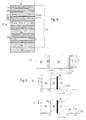
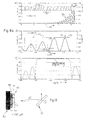
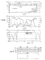
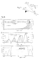
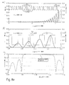
- FIGS. 8a to 8e show examples of different coating ensembles as variants to those of FIGS. 1 and 6 .
- the width of the individual layers can be seen from the "rectangular curve " in the respective partial illustrations ⁇ and ⁇ .
- its refractive index n is plotted.
- the coating ensembles of FIGS. 8a to 8e differ from one another in the top three layers.
- the free coating end - the transition to air - is referred to as "above”.
- the bottom part ⁇ shows the course of the reflection R of the entire coating ensemble in question over the wavelength lambda in micrometers ( ⁇ m) of the incident radiation.
- the uppermost layer 56 is a GaAs layer with an optical layer thickness of a half wavelength based on 1.064 ⁇ m (free space wavelength), which contains an absorber sublayer 57 made of InGaAs with a refractive index of n ⁇ 3.6.
- Free space wavelength is understood to mean the wavelength in free space (vacuum). In the layer concerned, however, the value of the wavelength changes accordingly in accordance with the existing refractive index.
- the position of the absorber sub-layer 57 is selected such that it lies in the maximum of the intensity profile of a resonator wave. This position and the entire normalized intensity curve 59a of the laser resonator wave in the coating ensemble are shown in the partial illustration ⁇ in FIG . 8a .
- An enlarged representation with respect to the coating thickness dimensions for the upper coating partial layers shows the partial image ⁇ in FIG . 8a . Analogous to the partial image ⁇ , the intensity curve is given here as 59b .
- FIG. 8b shows a coating ensemble analogous to FIG. 8a , but here the uppermost layer 60 is a GaAs layer with the optical layer thickness of a quarter wavelength in relation to 1.064 ⁇ m.
- the absorbing layer 61 is here also in this layer 60 , but at the location of an already falling intensity 62a or 62b .
- FIG . 8c Another coating variant is shown in FIG . 8c .
- the absorbent layer 63 is also embedded in the uppermost layer 64 .
- the top layer 64 is a layer with a low refractive index, namely n ⁇ 2.95 made of AlAs.
- the optical layer thickness corresponds to a half wavelength based on 1.064 ⁇ m.
- the absorbent layer 63 is arranged approximately in one of the intensity maxima, here in the absolute intensity maximum 65 .
- FIGS . 8d and 8e show further variants of coating ensembles .
- the absorbing layer 68 or 70 is no longer embedded in the uppermost layer, but in a lower one, here in the third uppermost layer 67 or 69 , for example.
- the absorbent layer 68 is approximately at the location of a relative intensity maximum.
- the absorbent layer 70 lies in the sloping part after a relative intensity maximum.
- FIGS. 8a to 8e show a way in which the optimal position of the saturable absorber in the coating ensemble can be found. With a careful selection of the absorber layer, a desired broad band in relation to the desired wavelength range can be achieved. In the examples shown, a range of 50 nm has been reached. Furthermore, the effective, ie seen from "outside" saturation intensity in the coating ensemble z. B. can be increased if the absorber is embedded deeper, as shown for example in FIG. 8d .
- a Ti: sapphire laser crystal (not shown) with a thickness of 2 mm is used as the active laser material.
- the resonator mirrors are arranged at a mutual distance of 10 cm, as a result of which the laser beam diameter in the absorbing layer described below is 36 ⁇ m.
- the coupling mirror (not shown) (one of the two resonator mirrors) couples 3% of the laser intensity out of the laser resonator.
- the coating ensembles shown in FIGS. 9b and 9c for use in the above-mentioned laser resonator, not shown have a metallic layer, here a silver layer.
- a metallic layer here a silver layer.
- other metal layers such as gold layers, can also be present.
- a 40 nm thick GaAs layer 73 is then applied to this layer 72 .
- There now follows a further 20 nm thick layer 74 made of Al x Ga 1-x As layer 72 with x 0.65.
- a 15 nm thick GaAs absorber layer 75 is applied to the layer 74 in a low-temperature process (400 ° C.), followed by a 70 nm thick AlAs layer 76 and a 3 nm thick GaAs layer 77 , which later oxidize the Layer 76 should avoid.
- a 5 ⁇ m thick silver layer 78 is then placed on the layer 77 .
- the coated substrate 71 is cut into pieces approximately 5 mm ⁇ 5 mm in size. These pieces are then adhered to a silicon substrate 80 with a two-component epoxy adhesive 79 in order to obtain sufficient heat dissipation. In a next process step, the pieces are heat treated at 80 ° C for eight hours under a surface weight of 500 g. Next, the GaAs substrate 71 is lapped down to 100 ⁇ m and etched with ammonia dissolved in hydrogen peroxide [NH 4 OH: H 2 O 2 (1:25)] at an etching rate at room temperature of about 6 ⁇ m per minute up to layer 72 . Layer 72 is then removed to layer 73 with hydrofluoric acid.
- Layer 73 is etched away analogously to layer 71 with ammonia of lower concentration dissolved in hydrogen peroxide [NH 4 OH: H 2 O 2 (1: 200)].
- the 5 mm x 5 mm pieces must be moved for a good, uniform etching.
- a wax application is used during the etching process.
- the wax protection layer can later be removed with trichloethylene.
- the top layer is now layer 74 .
- FIG. 9c The coating ensemble shown in FIG. 9c was produced analogously to that in FIG. 9b .
- Layers 83, 84, 85 and 86 correspond to layers 78, 77, 76 and 75 of the coating ensemble in FIG . 9b .
- FIGS. 9b and 9c each show the local course of the intensity with the reference numbers 91a and 91b .
- the coating ensemble shown in FIG. 9b works in the (not shown) laser resonator with low quality in anti-resonance. This avoids an ultrashort-pulse-width limitation, caused by an increased wavelength-dependent change in reflection and an increased group speed dispersion [see, for example, LRBrovelli, U. Keller, THChiu, J.Opt.Soc.Am. B 12, 311 (1995)].
- the reflection of the coating ensemble is greater than 94% at 800 nm.
- the reflection curve shows only a slight wavelength dependency in the range between 700 nm and 1200 nm.
- FIG . 10 shows an example of a coating ensemble with III-V semiconductor and fluoride layers for a laser wavelength of 1.4 ⁇ m.
- a GaAs quarter-wave layer 97a to 97c (100 nm layer thickness) is arranged between each of these "sandwiches”.
- a layer of GaAs 95 is deposited on a GaAs substrate 96 in a coating process. The layer 95 serves only to enable good holding and growth for the subsequent layers.
- the difference in refractive index between CaF 2 and BaF 2 is small, but BaF 2 has a large elastic constant, which greatly reduces the formation of cracks in the coating during the cooling process.
- Layers with a saturable absorber can also be integrated on or in this coating ensemble.
- AlGaAs is preferably used instead of GaAs; GaAs shows absorption below 900 nm.
- the advantage here is that the layers grow epitaxially on one another.
- GaAs, AlGaAs, InGaAs, GaInP, GaInAsP etc. can be used as semiconductor materials and CaF 2 , BaF 2 , SrF 2 , ... as fluorides.
- the resonator shown in FIG. 11 has a laser crystal 99 , through which an end 100 mirrored for the laser wavelength is pumped.
- the resonator shaft 101 generated with the laser crystal 99 is deflected via the deflection mirrors 102, 103 and 104 .
- the laser crystal 99 is optically pumped with the pump light beam 98 .
- the saturable absorber with one of the coating ensembles described above is arranged as a resonator end mirror 105 .
- the laser radiation is coupled out at the deflecting mirror 103 .
- the laser resonator according to FIG. 12 also has a saturable absorber in one of the coating ensembles described above.
- the coating ensemble 107 is integrated in the resonator end mirror.
- the resonator has an end mirror 112 and four deflecting mirrors 108 to 111 , the element 110 being an active medium (laser crystal) and a mirror at the same time.
- Laser energy is partially coupled out via the end mirror 112 .
- the optical pumping of the laser crystal 110 takes place via the pump light beam 114 .
- FIG . 13 shows a miniaturized laser resonator for generating short pulses analogous to the resonators already described above.
- a coating ensemble 115 with a saturable absorber is applied as a resonator end mirror according to one of the above-mentioned embodiments.
- the laser crystal 117 is placed directly on this coating ensemble 115 . (However, the crystal could also be provided with the coating ensemble at the point marked 116. )
- the thickness of approximately 200 ⁇ m of the laser crystal 117 plus the “penetration depth” of the radiation into the coating ensemble determine the resonator length.
- the coupling-out mirror 119 with a corresponding coating for the laser beam 121 to be coupled out and for coupling in the pump light beam 122 is arranged directly on the side of the laser crystal 117 opposite the ensemble 115 .
- Laser beam 121 and pump light beam 122 are separated from one another by a correspondingly coated beam splitter 123 .
Landscapes
- Physics & Mathematics (AREA)
- Nonlinear Science (AREA)
- Optics & Photonics (AREA)
- Engineering & Computer Science (AREA)
- Electromagnetism (AREA)
- General Physics & Mathematics (AREA)
- Chemical & Material Sciences (AREA)
- Materials Engineering (AREA)
- Nanotechnology (AREA)
- Plasma & Fusion (AREA)
- Lasers (AREA)
- Optical Elements Other Than Lenses (AREA)
Claims (11)
- Procédé pour la fabrication d'un composant optique avec un facteur de réflexion préétabli pour un rayonnement laser, de préférence utilisable pour la production de courte pulsion laser dans un résonateur laser, dans lequel il est d'abord déterminé une structure d'un ensemble de stratification sur la surface de substrat des composants (1; 42; 53, 55, 56, 57; 53, 55, 60, 61; 53, 55, 63, 64 ; 53, 55, 67, 68 ; 53, 55, 60, 70; 115, cet ensemble étant constitué par des premières et secondes couches (11, 13; 33, 34 ; 53, 55; 73, 74) et au moins une troisième couche contenant un matériau semiconducteur absorbant saturable pour le rayonnement laser (6, 39, 57, 61, 63, 68, 70, 75), les épaisseurs de couches et localisation des premières et secondes couches contenant le matériau absorbant saturable ainsi que de la troisième couche étant déterminée arithmétiquement, de sorte que le facteur de réflexion préétabli avec l'ensemble se trouvant sur la surface (1; 42 ; 53, 55, 56, 57; 53, 55, 60, 61; 53, 55, 63, 64 ; 53, 55, 67, 68 ; 53, 55, 60, 70 ; 115) et dans chaque troisième couche on obtient une valeur d'intensité de rayonnement normalisée préétablie pour le rayonnement laser à émettre, chaque valeur d'intensité de rayonnement étant sélectionnée de telle sorte que l'effet absorbant saturable souhaité pour la production des pulsations courtes est produite dans un résonateur laser (20, 23, 24a, 24b, 25a, 25b ; 43, 45, 47, 50a, 50b; 100, 99, 102, 103, 104, 105; 107, 108, 109, 110, 111, 112; 115, 117, 119), et conformément à ce calcul, on applique sur la surface des composants l'ensemble de couches (1 ; 42; 53, 55, 56, 57 ; 53, 55, 60, 61; 53, 55, 63, 64 ; 53, 55, 67, 68 ; 53, 55, 60, 70; 115) correspondant à la structure déterminée.
- Procédé selon la revendication 1, caractérisé en ce que le facteur de réflexion de l'ensemble de couches (1; 42; 53, 55, 56, 57 ; 53, 55, 60, 61; 53, 55, 63, 64 ; 53, 55, 67, 68 ; 53, 55, 60, 70 ; 115) est préétabli de telle sorte que l'ensemble de couches rend les composants antiréfléchissants comme compensation optique pour le rayonnement laser ou totalement réfléchissant, les composants pouvant alors être par exemple utilisés en tant que miroir de la cavité.
- Procédé selon la revendication 1 ou 2, caractérisé en ce qu'au moins l'une des trois couches (6, 39, 57, 61, 63, 68, 70) est disposée sur l'emplacement ou sur les emplacements de l'ensemble de couches, ou il est produit arithmétiquement un gradiant d'intensité de rayonnement élevée pour obtenir une modification d'absorption élevée dans au moins un domaine partiel de fréquence du rayonnement du résonateur.
- Procédé selon l'une des revendications 1 à 3, caractérisé en ce qu'en tant que matériau pour les couches de l'ensemble de couches (1; 42 ; 53, 55, 56, 57 ; 53, 55, 60, 61; 53, 55, 63, 64 ; 53, 55, 67, 68 ; 53, 55, 60, 70; 115) on a choisi des matériaux semiconducteurs, lesquels de préférence de l'arsenic, en particulier un métal ou dans une forme de réalisation particulière, au moins un fluorure en tant que partenaire de composition essentielle et en tant que matériau pour chaque troisième couche, un matériau à semiconducteur étant préféré, en particulier l'arséniure de gallium, l'arséniure de gallium aluminium ou un arséniure de gallium indium.
- Procédé selon l'une des revendications 1 à 4, caractérisé en ce que la séquence de couches de l'ensemble de couches est préétabli de telle sorte que pour un rayonnement laser incident, on obtient une dispersion de la vitesse de groupe.
- Procédé selon la revendication 5, caractérisé en ce qu'au moins dans une partie des couches de l'ensemble de couches (1; 42 ; 53, 55, 56, 57; 53, 55, 60, 61; 53, 55, 63, 64 ; 53, 55, 67, 68 ; 53, 55, 60, 70; 115) il est proposé comme matériau un matériau semiconducteur avec un pourcentage d'aluminium, la proportion d'aluminium étant préétablie de façon correspondante à la fréquence moyenne attendue du rayonnement du résonateur de sorte que dans la ou dans les couches prévues pour l'absorption saturable, on pourra produire une absorption saturable avec la vitesse de groupe négative requise pour la génération de pulsation en mode bloqué extrêmement courte.
- Laser pour la production de courte pulsation, en particulier dans le domaine des micros jusqu'à Femto secondes, caractérisé en ce qu'au moins un composant optique est formé dans le résonateur laser (20, 23, 24a, 24b, 25a, 25b, 43, 45, 47, 50a, 50b; 100, 99, 102, 104, 105; 107, 108, 109, 110, 111, 112; 115, 117, 119) avec un ensemble de couches optiques appliquées sur la surface de composant (1; 42, 53, 55, 56, 57; 53, 55, 60, 61; 53, 55, 63, 64 ; 53, 55, 67, 68 ; 53, 55, 60, 70; 115), avec des premières et secondes couches optiques et au moins une troisième couche de matériau à semiconducteurs, les premières et deuxième couches avoisinantes (11, 13 ; 33, 34 ; 53, 55 ; 73, 74) ayant un indice de réfraction optique variable et chaque troisième couche (6, 39, 57, 61, 63, 68, 70, 75) ayant un matériau absorbant saturable pour la longueur d'ondes du rayonnement laser, de sorte que les premières, deuxièmes et troisièmes couches sont disposées conjointement de façon accouplée par phase par leur agencement et leur épaisseur de couches de telle sorte que le composant a un facteur de réflexion préétabli pour le rayonnement lors de l'incidence et la troisième couche ou les troisièmes couches et/ou sont disposés (6, 39, 57, 61, 63, 68, 70, 75) en des lieux dans l'ensemble (1 ; 42 ; 53, 55, 56, 57 ; 53, 55, 60, 61 ; 53, 55, 63, 64 ; 53, 55, 67, 68 ; 53, 55, 60, 70 ; 115) sur lesquels on obtient une intensité normalisée préétablie lors de l'incidence du rayonnement sur le composant.
- Laser selon la revendication 7, caractérisé en ce que l'ensemble de couches (1 ; 42 ; 53, 55, 56, 57 ; 53, 55, 60, 61 ; 53, 55, 63, 64 ; 53, 55, 67, 68 ; 53, 55, 60, 70 ; 115) d'au moins un composant optique est formé de telle sorte que le rayonnement laser ne peut être réfléchi avec la longueur d'onde préétablie.
- laser selon la revendication 7, caractérisé en ce que l'ensemble de couches (1 ; 42 ; 53, 55, 56; 57 ; 53, 55, 60, 61 ; 53, 55, 63, 64 ; 53, 55, 67, 68 ; 53, 55, 60, 70 ; 115) d'au moins un composant est formé de telle sorte que le rayonnement laser peut être réfléchi en totalité avec la longueur d'onde préétablie, le composant étant utilisable comme miroir de cavité.
- Laser selon l'une des revendications 7 à 9, caractérisée en ce que les couches de l'ensemble de couches 1 ; 42; 53, 55, 56, 57; 53, 55, 60, 61; 53, 55, 63, 64 ; 53, 55, 67, 68 ; 53, 55, 60, 70; 115) d'au moins un composant optique sont pour l'essentiel constitués de matériaux semiconducteurs, qui contiennent de préférence de l'arsenic, en particulier un métal ou dans un mode de réalisation particulier au moins un fluorure en tant que partenaire de composition essentielle et chaque troisième couche est de préférence de l'arséniure de gallium, de l'arséniure de gallium aluminium ou un arséniure de gallium indium.
- Laser selon une des revendication 7 à 10, caractérisé en ce qu'au moins une partie des couches de l'ensemble de couches (1; 42; 53, 55, 56, 57; 53, 55, 60, 61; 53, 55, 63, 64 ; 53, 55, 67, 68 ; 53, 55, 60, 70; 115) d'au moins un composant optique possède comme matériau un semiconducteur avec un pourcentage en aluminium, le pourcentage en aluminium étant prédéterminé de façon correspondante à la fréquence moyenne attendue du rayonnement de résonateur de sorte que dans la troisième couche ou dans les troisièmes couches, on pourra obtenir une absorption saturable conjointement avec la dispersion de vitesse de groupe négative requise pour le rayonnement laser préétabli afin de pouvoir générer des pulsations extrêmement courtes en mode bloqué.
Applications Claiming Priority (3)
| Application Number | Priority Date | Filing Date | Title |
|---|---|---|---|
| CH1499/95 | 1995-05-19 | ||
| CH149995 | 1995-05-19 | ||
| PCT/CH1996/000185 WO1996036906A1 (fr) | 1995-05-19 | 1996-05-15 | Composant optique pour la production d'un rayonnement laser pulse |
Publications (2)
| Publication Number | Publication Date |
|---|---|
| EP0826164A1 EP0826164A1 (fr) | 1998-03-04 |
| EP0826164B1 true EP0826164B1 (fr) | 1999-03-31 |
Family
ID=4211888
Family Applications (1)
| Application Number | Title | Priority Date | Filing Date |
|---|---|---|---|
| EP96913414A Revoked EP0826164B1 (fr) | 1995-05-19 | 1996-05-15 | Composant optique pour la production d'un rayonnement laser pulse |
Country Status (5)
| Country | Link |
|---|---|
| US (1) | US6466604B1 (fr) |
| EP (1) | EP0826164B1 (fr) |
| JP (2) | JPH11505370A (fr) |
| DE (1) | DE59601560D1 (fr) |
| WO (1) | WO1996036906A1 (fr) |
Cited By (1)
| Publication number | Priority date | Publication date | Assignee | Title |
|---|---|---|---|---|
| US6944201B2 (en) | 1999-07-30 | 2005-09-13 | High Q Laser Production Gmbh | Compact ultra fast laser |
Families Citing this family (23)
| Publication number | Priority date | Publication date | Assignee | Title |
|---|---|---|---|---|
| DE19934639A1 (de) | 1999-07-23 | 2001-02-01 | Ldt Gmbh & Co | Resonatorspiegel mit einem sättigbaren Absorber |
| WO2001043242A1 (fr) * | 1999-12-08 | 2001-06-14 | Time-Bandwidth Products Ag | Laser a disque fin a modes bloques |
| US7247892B2 (en) * | 2000-04-24 | 2007-07-24 | Taylor Geoff W | Imaging array utilizing thyristor-based pixel elements |
| US6538298B1 (en) * | 2001-12-10 | 2003-03-25 | Gigatera Ag | Semiconductor saturable absorber mirror |
| US7218443B2 (en) * | 2003-02-25 | 2007-05-15 | Toptica Photonics Ag | Generation of tunable light pulses |
| WO2005020305A2 (fr) * | 2003-08-12 | 2005-03-03 | Massachusetts Institute Of Technology | Dispositif optique comprenant une couche cristalline a semi-conducteur et un element reflechissant |
| US7133426B2 (en) * | 2004-02-24 | 2006-11-07 | Ekspla Ltd. | Method and apparatus for producing a pulsed laser beam |
| US7386019B2 (en) | 2005-05-23 | 2008-06-10 | Time-Bandwidth Products Ag | Light pulse generating apparatus and method |
| EP1870972A1 (fr) * | 2006-06-22 | 2007-12-26 | Fujifilm Corporation | Dispositif laser à mode couplé |
| JP2008028379A (ja) * | 2006-06-22 | 2008-02-07 | Fujifilm Corp | モードロックレーザ装置 |
| DE102007034289B3 (de) | 2007-07-20 | 2009-01-29 | Helmholtz-Zentrum Berlin Für Materialien Und Energie Gmbh | Verfahren zur in-situ-Bestimmung der stofflichen Zusammensetzung von optisch dünnen Schichten, Anordnungen zur Durchführung und Anwendungen des Verfahrens |
| DE102008013925B3 (de) * | 2008-03-12 | 2009-05-07 | Batop Gmbh | Sättigbarer Absorberspiegel mit einem Luftspalt |
| WO2013152447A2 (fr) | 2012-04-11 | 2013-10-17 | Time-Bandwidth Products Ag | Laser semi-conducteur pulsé |
| US8724666B1 (en) * | 2013-01-04 | 2014-05-13 | Alcon Lensx, Inc. | Self starting mode-locked laser oscillator |
| DE102014114732B4 (de) * | 2014-10-10 | 2016-06-02 | Trumpf Laser Gmbh | Verfahren zum anbringen eines sättigbaren halbleiter-absorberelements auf einem träger und halbleiter-absorberelement-einheit |
| US11466316B2 (en) | 2015-05-20 | 2022-10-11 | Quantum-Si Incorporated | Pulsed laser and bioanalytic system |
| US10605730B2 (en) | 2015-05-20 | 2020-03-31 | Quantum-Si Incorporated | Optical sources for fluorescent lifetime analysis |
| EP3555972A1 (fr) | 2016-12-16 | 2019-10-23 | Quantum-si Incorporated | Module laser compact à verrouillage de mode |
| KR102805796B1 (ko) | 2016-12-16 | 2025-05-15 | 퀀텀-에스아이 인코포레이티드 | 콤팩트한 빔 셰이핑 및 스티어링 어셈블리 |
| EP3807622A1 (fr) | 2018-06-15 | 2021-04-21 | Quantum-Si Incorporated | Commande d'acquisition de données pour instruments analytiques perfectionnés ayant des sources optiques pulsées |
| AU2020294144A1 (en) | 2019-06-14 | 2022-01-27 | Quantum-Si Incorporated | Sliced grating coupler with increased beam alignment sensitivity |
| IL294734A (en) | 2020-01-14 | 2022-09-01 | Quantum Si Inc | Amplitude-modulated laser |
| CN118249213B (zh) * | 2024-04-08 | 2024-11-05 | 重庆师范大学 | 一种多芯片超快激光器 |
Family Cites Families (7)
| Publication number | Priority date | Publication date | Assignee | Title |
|---|---|---|---|---|
| US4860296A (en) | 1983-12-30 | 1989-08-22 | American Telephone And Telegraph Company, At&T Bell Laboratories | Laser controlled by a multiple-layer heterostructure |
| WO1985003171A1 (fr) | 1983-12-30 | 1985-07-18 | American Telephone & Telegraph Company | Laser regule par une heterostructure a couches multiples |
| US5345454A (en) | 1991-11-06 | 1994-09-06 | At&T Bell Laboratories | Antiresonant Fabry-Perot p-i-n modulator |
| US5237577A (en) | 1991-11-06 | 1993-08-17 | At&T Bell Laboratories | Monolithically integrated fabry-perot saturable absorber |
| US5265107A (en) | 1992-02-05 | 1993-11-23 | Bell Communications Research, Inc. | Broadband absorber having multiple quantum wells of different thicknesses |
| US5278855A (en) * | 1992-05-11 | 1994-01-11 | At&T Bell Laboratories | Broadband semiconductor saturable absorber |
| US5627854A (en) * | 1995-03-15 | 1997-05-06 | Lucent Technologies Inc. | Saturable bragg reflector |
-
1996
- 1996-05-15 DE DE59601560T patent/DE59601560D1/de not_active Revoked
- 1996-05-15 US US08/952,478 patent/US6466604B1/en not_active Expired - Lifetime
- 1996-05-15 WO PCT/CH1996/000185 patent/WO1996036906A1/fr not_active Ceased
- 1996-05-15 EP EP96913414A patent/EP0826164B1/fr not_active Revoked
- 1996-05-15 JP JP8534427A patent/JPH11505370A/ja active Pending
-
2007
- 2007-11-21 JP JP2007302122A patent/JP2009277676A/ja active Pending
Cited By (1)
| Publication number | Priority date | Publication date | Assignee | Title |
|---|---|---|---|---|
| US6944201B2 (en) | 1999-07-30 | 2005-09-13 | High Q Laser Production Gmbh | Compact ultra fast laser |
Also Published As
| Publication number | Publication date |
|---|---|
| EP0826164A1 (fr) | 1998-03-04 |
| JPH11505370A (ja) | 1999-05-18 |
| US6466604B1 (en) | 2002-10-15 |
| DE59601560D1 (de) | 1999-05-06 |
| JP2009277676A (ja) | 2009-11-26 |
| WO1996036906A1 (fr) | 1996-11-21 |
Similar Documents
| Publication | Publication Date | Title |
|---|---|---|
| EP0826164A1 (fr) | Composant optique pour la production d'un rayonnement laser pulse | |
| EP2577818B1 (fr) | Laser micro-puce à impulsions ultra-courtes, laser semi-conducteur, système laser et procédé de pompage pour milieux laser minces | |
| EP0732613B1 (fr) | Laser avec un réflecteur de Bragg saturable | |
| DE69207862T2 (de) | Monolitisch integrierter Fabry-Perot sättigbarer Absorber | |
| DE60002165T2 (de) | Festkörperlaser mit passiver modenkopplung und hoher pulswiederholfrequenz | |
| DE60120651T2 (de) | Optisch gepumpter passiv modengekoppelter oberflächenemittierender halbleiterlaser mit externem resonator | |
| DE69614310T2 (de) | Monolitische Halbleiterinfrarotsender, optisch gepumpt durch einen gütegeschalteten Festkörpermikrolaser | |
| US5701327A (en) | Saturable Bragg reflector structure and process for fabricating the same | |
| DE69424552T2 (de) | Tiefblauer mikrolaser | |
| JP2724279B2 (ja) | レーザシステム | |
| DE69419999T2 (de) | Optimierung der Emissionscharakteristik eines Lasers mit externem Resonator | |
| DE60212436T2 (de) | Kompakte Festkörperlaser | |
| DE102008013925B3 (de) | Sättigbarer Absorberspiegel mit einem Luftspalt | |
| WO2018224483A1 (fr) | Laser à semi-conducteur à émission par la tranche et procédé de fonctionnement d'un tel laser à semi-conducteur | |
| US6826219B2 (en) | Semiconductor saturable absorber device, and laser | |
| EP1456916B1 (fr) | Dispositif miroir absorbeur saturable a semi-conducteur | |
| JPH08262380A (ja) | 非共鳴ファブリ・ペローpin変調装置 | |
| US6141359A (en) | Modelocking laser including self-tuning intensity-dependent reflector for self-starting and stable operation | |
| EP1079483B1 (fr) | Miroir de cavité avec absorbant saturable | |
| DE10030672B4 (de) | Sättigbare Reflektoreinheit und sättigbarer Absorber | |
| US5901162A (en) | Hybrid, saturable reflector for mode-locking lasers | |
| DE102008061335B4 (de) | Sättigbarer Absorberspiegel und Verfahren zur Anpassung eines sättigbaren Absorberspiegels an eine vorgegebene Arbeitswellenlänge | |
| DE4242862C2 (de) | Optisch oder elektrisch gepumpter Festkörperlaser | |
| DE4239654C1 (de) | Laserdiodengepumpter Mikrokristall-Festkörperlaser | |
| WO2006122727A1 (fr) | Absorbeur saturable destine a un laser a modes bloques passivement |
Legal Events
| Date | Code | Title | Description |
|---|---|---|---|
| PUAI | Public reference made under article 153(3) epc to a published international application that has entered the european phase |
Free format text: ORIGINAL CODE: 0009012 |
|
| 17P | Request for examination filed |
Effective date: 19971201 |
|
| AK | Designated contracting states |
Kind code of ref document: A1 Designated state(s): CH DE FR GB IT LI |
|
| 17Q | First examination report despatched |
Effective date: 19980206 |
|
| GRAG | Despatch of communication of intention to grant |
Free format text: ORIGINAL CODE: EPIDOS AGRA |
|
| GRAG | Despatch of communication of intention to grant |
Free format text: ORIGINAL CODE: EPIDOS AGRA |
|
| GRAH | Despatch of communication of intention to grant a patent |
Free format text: ORIGINAL CODE: EPIDOS IGRA |
|
| GRAH | Despatch of communication of intention to grant a patent |
Free format text: ORIGINAL CODE: EPIDOS IGRA |
|
| GRAA | (expected) grant |
Free format text: ORIGINAL CODE: 0009210 |
|
| AK | Designated contracting states |
Kind code of ref document: B1 Designated state(s): CH DE FR GB IT LI |
|
| REG | Reference to a national code |
Ref country code: CH Ref legal event code: EP |
|
| ITF | It: translation for a ep patent filed | ||
| REF | Corresponds to: |
Ref document number: 59601560 Country of ref document: DE Date of ref document: 19990506 |
|
| REG | Reference to a national code |
Ref country code: CH Ref legal event code: NV Representative=s name: KELLER & PARTNER PATENTANWAELTE AG |
|
| RAP2 | Party data changed (patent owner data changed or rights of a patent transferred) |
Owner name: TIME-BANDWIDTH PRODUCTS AG |
|
| ET | Fr: translation filed | ||
| GBT | Gb: translation of ep patent filed (gb section 77(6)(a)/1977) |
Effective date: 19990803 |
|
| PLBQ | Unpublished change to opponent data |
Free format text: ORIGINAL CODE: EPIDOS OPPO |
|
| PLBI | Opposition filed |
Free format text: ORIGINAL CODE: 0009260 |
|
| 26 | Opposition filed |
Opponent name: KOPF, DANIEL, DR. Effective date: 20000103 Opponent name: JENOPTIK AG Effective date: 19991229 |
|
| PLBF | Reply of patent proprietor to notice(s) of opposition |
Free format text: ORIGINAL CODE: EPIDOS OBSO |
|
| PLBF | Reply of patent proprietor to notice(s) of opposition |
Free format text: ORIGINAL CODE: EPIDOS OBSO |
|
| PLBF | Reply of patent proprietor to notice(s) of opposition |
Free format text: ORIGINAL CODE: EPIDOS OBSO |
|
| PLBF | Reply of patent proprietor to notice(s) of opposition |
Free format text: ORIGINAL CODE: EPIDOS OBSO |
|
| REG | Reference to a national code |
Ref country code: CH Ref legal event code: PUE Owner name: TIME-BANDWIDTH PRODUCTS AG TRANSFER- GIGATERA AG |
|
| REG | Reference to a national code |
Ref country code: GB Ref legal event code: 732E |
|
| REG | Reference to a national code |
Ref country code: FR Ref legal event code: TP |
|
| REG | Reference to a national code |
Ref country code: GB Ref legal event code: IF02 |
|
| PLBQ | Unpublished change to opponent data |
Free format text: ORIGINAL CODE: EPIDOS OPPO |
|
| PLAB | Opposition data, opponent's data or that of the opponent's representative modified |
Free format text: ORIGINAL CODE: 0009299OPPO |
|
| R26 | Opposition filed (corrected) |
Opponent name: JENOPTIK AG * 20000103 KOPF, DANIEL, DR. Effective date: 19991229 |
|
| RAP2 | Party data changed (patent owner data changed or rights of a patent transferred) |
Owner name: GIGATERA AG |
|
| RAP2 | Party data changed (patent owner data changed or rights of a patent transferred) |
Owner name: GIGATERA AG |
|
| RDAH | Patent revoked |
Free format text: ORIGINAL CODE: EPIDOS REVO |
|
| APAC | Appeal dossier modified |
Free format text: ORIGINAL CODE: EPIDOS NOAPO |
|
| APAC | Appeal dossier modified |
Free format text: ORIGINAL CODE: EPIDOS NOAPO |
|
| REG | Reference to a national code |
Ref country code: GB Ref legal event code: 732E |
|
| REG | Reference to a national code |
Ref country code: CH Ref legal event code: PLI Owner name: TIME-BANDWIDTH PRODUCTS AG Free format text: GIGATERA AG#LERZENSTRASSE 16#8953 DIETIKON (CH) -TRANSFER TO- TIME-BANDWIDTH PRODUCTS AG#TECHNOPARKSTRASSE 1#8005 ZUERICH (CH) |
|
| REG | Reference to a national code |
Ref country code: FR Ref legal event code: CL |
|
| APAA | Appeal reference recorded |
Free format text: ORIGINAL CODE: EPIDOS REFN |
|
| PGFP | Annual fee paid to national office [announced via postgrant information from national office to epo] |
Ref country code: GB Payment date: 20050506 Year of fee payment: 10 |
|
| PG25 | Lapsed in a contracting state [announced via postgrant information from national office to epo] |
Ref country code: IT Free format text: LAPSE BECAUSE OF NON-PAYMENT OF DUE FEES Effective date: 20050515 |
|
| PGFP | Annual fee paid to national office [announced via postgrant information from national office to epo] |
Ref country code: FR Payment date: 20050517 Year of fee payment: 10 |
|
| PGFP | Annual fee paid to national office [announced via postgrant information from national office to epo] |
Ref country code: DE Payment date: 20050525 Year of fee payment: 10 |
|
| PGFP | Annual fee paid to national office [announced via postgrant information from national office to epo] |
Ref country code: CH Payment date: 20050530 Year of fee payment: 10 |
|
| APAH | Appeal reference modified |
Free format text: ORIGINAL CODE: EPIDOSCREFNO |
|
| APBU | Appeal procedure closed |
Free format text: ORIGINAL CODE: EPIDOSNNOA9O |
|
| RDAG | Patent revoked |
Free format text: ORIGINAL CODE: 0009271 |
|
| STAA | Information on the status of an ep patent application or granted ep patent |
Free format text: STATUS: PATENT REVOKED |
|
| REG | Reference to a national code |
Ref country code: CH Ref legal event code: PL |
|
| 27W | Patent revoked |
Effective date: 20051109 |
|
| GBPR | Gb: patent revoked under art. 102 of the ep convention designating the uk as contracting state |
Free format text: 20051109 |
|
| PLAB | Opposition data, opponent's data or that of the opponent's representative modified |
Free format text: ORIGINAL CODE: 0009299OPPO |