EP0827004A2 - Korrigiertes optisches Abtastgerät - Google Patents
Korrigiertes optisches Abtastgerät Download PDFInfo
- Publication number
- EP0827004A2 EP0827004A2 EP97114861A EP97114861A EP0827004A2 EP 0827004 A2 EP0827004 A2 EP 0827004A2 EP 97114861 A EP97114861 A EP 97114861A EP 97114861 A EP97114861 A EP 97114861A EP 0827004 A2 EP0827004 A2 EP 0827004A2
- Authority
- EP
- European Patent Office
- Prior art keywords
- optical element
- diffracting
- scanning
- scanning optical
- scanning direction
- Prior art date
- Legal status (The legal status is an assumption and is not a legal conclusion. Google has not performed a legal analysis and makes no representation as to the accuracy of the status listed.)
- Granted
Links
Images





Classifications
-
- G—PHYSICS
- G02—OPTICS
- G02B—OPTICAL ELEMENTS, SYSTEMS OR APPARATUS
- G02B26/00—Optical devices or arrangements for the control of light using movable or deformable optical elements
- G02B26/08—Optical devices or arrangements for the control of light using movable or deformable optical elements for controlling the direction of light
- G02B26/10—Scanning systems
- G02B26/12—Scanning systems using multifaceted mirrors
- G02B26/125—Details of the optical system between the polygonal mirror and the image plane
-
- G—PHYSICS
- G02—OPTICS
- G02B—OPTICAL ELEMENTS, SYSTEMS OR APPARATUS
- G02B27/00—Optical systems or apparatus not provided for by any of the groups G02B1/00 - G02B26/00, G02B30/00
- G02B27/0025—Optical systems or apparatus not provided for by any of the groups G02B1/00 - G02B26/00, G02B30/00 for optical correction, e.g. distorsion, aberration
- G02B27/0031—Optical systems or apparatus not provided for by any of the groups G02B1/00 - G02B26/00, G02B30/00 for optical correction, e.g. distorsion, aberration for scanning purposes
Definitions
- This invention relates to a scanning optical apparatus, and particularly to a scanning optical apparatus suitable for use in an apparatus such as a laser beam printer (LBP) having an electrophotographic process or a digital copying apparatus designed to deflect a light beam emitted from light source means comprising a semiconductor laser by a deflecting element, and optically scan a surface to be scanned through a scanning optical element (an imaging element) having the f ⁇ characteristic to thereby record image information.
- LBP laser beam printer
- an imaging element an imaging element
- a light beam optically modulated and emitted from light source means in conformity with an image signal is periodically deflected by a light deflector comprising, for example, a rotatable polygon mirror, and is converged into a spot-like shape on the surface of a photosensitive recording medium (a photosensitive drum) by a scanning optical element (an imaging element) having the f ⁇ characteristic, and the surface is optically scanned to thereby effect image recording.
- Fig. 1 of the accompanying drawings is a schematic view of the essential portions of a scanning optical apparatus of this kind according to the prior art.
- a divergent light beam emitted from light source means 21 is substantially collimated by a collimator lens 22, and this light beam (the quantity of light) is limited by a stop 23 and enters a cylindrical lens 24 having predetermined refractive power only in a sub-scanning direction.
- the light beam In the main scanning cross-section of the parallel light beam which has entered the cylindrical lens 24, the light beam emerges therefrom intactly as a parallel light beam.
- the light beam converges and is formed as a substantially linear image on the deflecting surface (reflecting surface) 25a of a light deflector 25 comprising a rotatable polygon mirror.
- the main scanning cross-section refers to a light beam cross-section formed with time by a light beam deflected and reflected by the deflecting surface of the light deflector.
- the sub-scanning cross-section refers to a cross-section containing the optical axis of an f ⁇ lens and orthogonal to the main scanning cross-section.
- the light beam deflected by the deflecting surface 25a of the light deflector 25 is directed to a photosensitive drum surface 28 as a surface to be scanned through a scanning optical element (f ⁇ lens) 26 having the f ⁇ characteristic, and the light deflector 25 is rotated in the direction of arrow A, whereby the photosensitive drum surface 28 is optically scanned in the direction of arrow B. Thereby, image recording is effected on the photosensitive drum surface 28 which is a recording medium.
- a scanning optical element (f ⁇ lens) 26 having the f ⁇ characteristic
- the scanning optical element (f ⁇ lens) in the scanning optical apparatus of this kind has become the mainstream from the requirements for a low price and compactness.
- the plastic lens has the nature that its refractive index varies with the fluctuation (temperature fluctuation) of its use environment and therefore, in a scanning optical apparatus using an f ⁇ lens comprising the plastic lens, changes in the magnification in the main scanning direction and changes in focus due to the fluctuation of the environment are caused.
- Fig. 2 of the accompanying drawings is a cross-sectional view (main scanning cross-sectional view) of the essential portions of a comparative example of the scanning optical apparatus in the main scanning direction thereof for illustrating such problem, and Table 1 below shows the optical arrangement and the aspherical coefficient of the f ⁇ lens in the comparative example.
- Fig. 3 of the accompanying drawings is an illustration showing the curvature of image field, the aberration of distortion and image height deviation in the main scanning direction of this scanning optical apparatus, and the solid lines indicate the characteristics at room temperature (25°C), and the dotted lines indicate the characteristics when a temperature rise to 50°C arose.
- the same elements as those shown in Fig. 1 are given the same reference characters.
- the scanning optical apparatus of the present invention comprises:
- the scanning optical apparatus is characterized in that the environmental fluctuations are temperature fluctuation and a wavelength fluctuation of the semiconductor laser, and the characteristic is the power ratio between the refracting portion and diffracting portion of the optical means.
- the scanning optical apparatus is characterized in that when the optical means is a scanning optical element for directing the light beam deflected by the deflecting element onto the surface to be scanned, changes in magnification and changes in focus in the main scanning direction resulting from the environmental fluctuations of the scanning optical apparatus are corrected by the characteristic of the scanning optical element.
- the scanning optical apparatus is characterized in that when the powers of the refractive portion and the diffracting portion of the scanning optical element are ⁇ L and ⁇ D, respectively, the condition that 1.0 ⁇ ⁇ L/ ⁇ D ⁇ 2.6 is satisfied,
- the scanning optical apparatus is characterized in that the optical means is an anamorphic optical element having a diffracting portion and for imaging the light beam emitted from the light source means into a linear shape long in the main scanning direction on the deflecting surface of the deflecting element, and a scanning optical element having a refracting portion for directing the light beam deflected by the deflecting element onto the surface to be scanned, and
- the scanning optical apparatus is characterized in that the characteristic is the power ratio between the diffracting portion of the anamorphic optical element and the refracting portion of the scanning optical element,
- the scanning optical apparatus is characterized in that the optical means is a converting optical element having a diffracting portion and for converting the light beam emitted from the light source means into a substantially parallel light beam, and a scanning optical element having a refracting portion for directing the light beam deflected by the deflecting element onto the surface to be scanned, and
- the scanning optical apparatus is characterized in that the characteristic is the power ratio between the diffracting portion of the converting optical element and the refracting portion of the scanning optical element,
- Fig. 1 is a schematic view of the essential portions of a scanning optical apparatus according to the prior art.
- Fig. 2 is a cross-sectional view of the essential portions of the scanning optical apparatus according to the prior art in the main scanning direction.
- Fig. 3 shows curvature of image field, aberration of distortion and image height deviation in the main scanning direction before and after temperature rise in the scanning optical apparatus according to the prior art.
- Fig. 4 is a cross-sectional view of the essential portions of Embodiment 1 of the present invention is the main scanning direction.
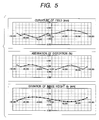
- Fig. 5 shows curvature of image field, aberration of distortion and image height deviation in the main scanning direction before and after temperature rise in Embodiment 1 of the present invention.
- Fig. 6 is a cross-sectional view of the essential portions of Embodiment 2 of the present invention in the main scanning direction.
- Fig. 7 shows curvature of image field, aberration of distortion and image height deviation in the main scanning direction before and after temperature rise in Embodiment 2 of the present invention.
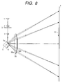
- Fig. 8 is a cross-sectional view of the essential portions of Embodiment 3 of the present invention in the main scanning direction.
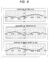
- Fig. 9 shows curvature of image field, aberration of distortion and image height deviation in the main scanning direction before and after temperature rise in Embodiment 3 of the present invention.
- Fig. 10 is a cross-sectional view of the essential portions of Embodiment 4 of the present invention in the main scanning direction.
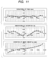
- Fig. 11 shows curvature of image field, aberration of distortion and image height deviation in the main scanning direction before and after temperature rise in embodiment 4 of the present invention.
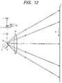
- Fig. 12 is a cross-sectional view of the essential portions of Embodiment 5 of the present invention in the main scanning direction.
- Fig. 4 is a cross-sectional view (main scanning cross-sectional view) of the essential portions of a scanning optical apparatus according to Embodiment 1 of the present invention for use in a laser beam printer in the main scanning direction.
- reference numeral 1 designates light source means comprising, for example, a semiconductor laser.
- Reference numeral 2 denotes a collimator lens which converts a divergent light beam emitted from the light source means 1 into a parallel light beam.
- Reference numeral 3 designates an aperture stop which limits the passing light beam (the quantity of light).
- Reference numeral 4 denotes a cylindrical lens (cylinder lens) which has predetermined refractive power only in a sub-scanning direction perpendicular to the plane of the drawing sheet of Fig. 4, and which images the light beam passed through the aperture stop 3 as a substantially linear image in a sub-scanning cross-section on the deflecting surface 5a of a light deflector 5 to be described below.
- Reference numeral 5 denotes a light deflector comprising, for example, a polygon mirror (rotatable polygon mirror) as a deflecting element, and being rotated at a predetermined speed in the direction of arrow A by driving means (not shown) such as a motor.
- driving means such as a motor.
- Reference numeral 6 designates a scanning optical element having the f ⁇ characteristic and having a refracting portion 6a and a diffracting portion 6b.
- the refracting porion 6a comprises a single lens (f ⁇ lens) formed of a plastic material, and the both lens surfaces of the single lens 6a in the main scanning direction comprise an aspherical shape. Also, the single lens 6a differs in refractive power between the main scanning direction and the sub-scanning direction.
- the diffracting portion 6b comprises a diffracting optical element, and comprises, for example, a binary diffracting optical element comprising a staircase-like diffraction grating by photoetching, or a Fresnel-like diffracting optical element comprising a sawtooth-like diffraction grating by surface cutting.
- the diffracting optical element 6b is added to at least one (the surface to be scanned side) of the both lens surfaces of the single lens 6a, and design is made such that the power (refractive power) ratio between the refracting portion 6a and the diffracting portion 6b is all within the range of expression (1) which will be described later from the on-axis toward the off-axis.
- the scanning optical element 6 causes a light beam based on image information deflected by the light deflector 5 to be imaged on a photosensitive drum surface 8 which is a recording medium and a surface to be scanned, and corrects the surface inclination of the deflecting surface of the light deflector 5.
- a divergent light beam emitted from the semiconductor laser 1 is converted into a substantially parallel light beam by the collimator lens 2, and this light beam (the quantity of light) is limited by the aperture stop 3 and enters the cylindrical lens 4.
- the light beam converges and is imaged as a substantially linear image (a linear image long in the main scanning direction) on the deflecting surface 5a of the light deflector 5.
- the light beam deflected by the deflecting surface 5a of the light deflector 5 is then directed onto the photosensitive drum surface 8 through the scanning optical element 6, and this light deflector 5 is rotated in the direction of arrow A to thereby optically scan the photosensitive drum surface 8 in the direction of arrow B. Thereby, image recording is effected on the photosensitive drum surface 8 which is a recording medium.
- the shapes of the single lens (f ⁇ lens) 6a constituting the scanning optical element 6 in the present embodiment and the diffracting optical element 6b added to that lens surface of the single lens 6a which is located at a side of the surface 8 to be scanned are as follows:
- Conditional expression (1) relates to the ratio between the power of the refracting portion 6a constituting the scanning optical element 6 and the power of the diffracting portion 6b also constituting the scanning optical element 6, and if conditional expression (1) is deviated from, it will become difficult to correct the changes in the magnification and focus in the main scanning direction resulting from the environmental fluctuations of the scanning optical apparatus, and this is not preferable.
- Table 2 below shows the optical arrangement in the present embodiment, the aspherical surface coefficient of the f ⁇ lens 6a and the phase term of the diffracting optical element (BOE) 6b.
- Fig. 5 is an illustration showing curvature of image field, aberration of distortion (f ⁇ characteristic) and image height deviation in the main scanning direction before and after temperature rise in the present embodiment, and the solid lines indicate the characteristics at room temperature (25°C) and the dotted lines indicate the characteristics when temperature has risen by 25°C and has reached 50°C. It is seen from Fig. 5 that there is little or no change in focus and magnification in the main scanning direction before and after the temperature rise (in Fig. 5, the difference between before and after the temperature rise is minute and therefore the graphs before and after the temperature rise overlap each other).
- the scanning optical element 6 is comprised of the refracting portion 6a comprising a lens and the diffracting portion 6b comprising a diffracting optical element, and the power ratio between the refracting portion 6a and the diffracting portion 6b is set to a suitable value so as to satisfy the above-mentioned conditional expression (1), whereby changes in the magnification and focus in the main scanning direction resulting from the environmental fluctuations of the scanning optical apparatus (temperature fluctuation and the wavelength fluctuation of the semiconductor laser) are corrected by the changes in the power of the refracting portion 6a and the diffracting portion 6b.
- a scanning optical apparatus which is strong against the environmental fluctuations and moreover is suited for highly minute printing is obtained compactly and inexpensively.
- Fig. 6 is a cross-sectional view (main scanning cross-sectional view) of the essential portions of Embodiment 2 of the present invention in the main scanning direction.
- Fig. 6 the same elements as those shown in Fig. 4 are given the same reference numerals.
- the material of the refracting portion (f ⁇ lens) 36a of a scanning optical element 36 is a plastic material of high refractive index as compared with that in Embodiment 1 and that correspondingly thereto, the power ratio of the refracting portion 36a and the diffracting portion (diffracting optical element) 36b of the scanning optical element 36 is made to differ.
- the construction and optical action of the present embodiment are substantially similar to those of the aforedescribed Embodiment 1, whereby there is obtained a similar effect.
- Table 3 shows the optical arrangement in the present embodiment, the aspherical surface coefficient of the f ⁇ lens 36a and the phase term of the diffracting optical element (BOE) 36b.
- Fig. 7 is an illustration showing curvature of image field, aberration of distortion (f ⁇ characteristic) and image height deviation in the main scanning direction before and after temperature rise in the present embodiment, and the solid lines indicate the characteristics at room temperature (25°C) and the dotted lines indicate the characteristics when temperature has risen by 25°C and has reached 50°C. It is seen from Fig. 7 that there is little or no change in the focus and magnification in the main scanning direction before and after the temperature rise.
- the material of the refracting portion (f ⁇ lens) 36a is a material of high refractive index as compared with that in Embodiment 1
- the power ratio between the refracting portion 36a and the diffracting portion 36b is set to a suitable value so as to satisfy the aforementioned conditional expression (1), whereby as in Embodiment 1, changes in the magnification and focus in the main scanning direction resulting from the environmental fluctuations (temperature fluctuation and the wavelength fluctuation of the semiconductor laser) of the scanning optical apparatus can be corrected by changes in the power of the refracting portion 36a and the diffracting portion 36b.
- the refracting portion (f ⁇ lens) 36a is constructed by the use of a material of high refractive index and therefore, the center thickness of the refracting portion 36a can be made small, whereby a further reduction in price can be achieved.
- Fig. 8 is a cross-sectional view (main scanning cross-sectional view) of the essential portions of Embodiment 3 of the present invention in the main scanning direction.
- Fig. 8 the same elements as these shown in Fig. 4 are given the same reference numerals.
- the material of the refracting portion (f ⁇ lens) 56a of a scanning optical element 56 is a plastic material of low refractive index as compared with that in Embodiment 1, and that correspondingly thereto, the power ratio between the refracting portion 56a and the diffracting portion (diffracting optical element) 56b of the scanning optical element 56 is made to differ.
- the construction and optical action of the present embodiment are substantially similar to those of the aforedescribed Embodiment 1, whereby there is obtained a similar effect.
- Table 4 below shows the optical arrangement in the present embodiment and the aspherical surface coefficient of the f ⁇ lens and the phase term of the diffracting optical element (BOE) 56b.
- Fig. 9 is an illustration showing curvature of image field, aberration of distortion (f ⁇ characteristic) and image height deviation in the main scanning direction before and after temperature rise in the present embodiment, and the solid lines indicate the characteristics at room temperature (25°C), and the dotted lines indicate the characteristics when temperature has risen by 25°C and reached 50°C. From Fig. 9, it is seen that there is little or no change in focus and magnification in the main scanning direction before and after the temperature rise.
- the material of the refracting portion (f ⁇ lens) 56a is a material of low refractive index as compared with that in Embodiment 1
- the power ratio between the refracting portion 56a and the diffracting portion 56b is set to a suitable value so as to satisfy the aforementioned conditional expression (1), whereby as in Embodiment 1, changes in the magnification and focus in the main scanning direction resulting from the environmental fluctuations (temperature fluctuation and the wavelength fluctuation of the semiconductor laser) of the scanning optical apparatus can be corrected by changes in the power of the refracting portion 56a and the diffracting portion 56b.
- Fig. 10 is a cross-sectional view (main scanning cross-sectional view) of the essential portions of Embodiment 4 of the present invention in the main scanning direction.
- Fig. 10 the same elements as those shown in Fig. 4 are given the same reference numerals.
- a diffracting optical element 74b as the diffracting portion is added to one surface of a cylindrical lens 74a for the correction of surface inclination, instead of an f ⁇ lens.
- the construction and optical action of the present embodiment are substantially similar to those of the aforedescribed Embodiment 1.
- the diffracting portion is added to the cylindrical lens, changes in the focus in the main scanning direction can be corrected, but changes in the magnification cannot be corrected.
- the size of the diffracting portion becomes small, and this leads to a reduced cost.
- reference numeral 74 designates an anamorphic optical element for correction of surface inclination
- this anamorphic optical element 74 has a refracting portion 74a and a diffracting portion 74b.
- the refracting portion 74a comprises a cylindrical lens (plano-convex lens) having no power in the main scanning direction
- the diffracting portion 74b comprises a diffracting optical element such as a binary optical element comprising the aforedescribed staircase-like diffraction grating or a Fresnel-like optical element comprising a sawtooth-like diffraction grating, and the diffracting optical element 74b is added to that lens surface of the cylindrical lens 74a, which is located the light deflector 5 side.
- Reference numeral 76 denotes a scanning optical element having the f ⁇ characteristic, and it comprises a single lens (f ⁇ lens) formed of a plastic material, and the both lens surfaces of the single lens 76 in the main scanning direction are formed of an aspherical shape. Also, the single lens 76 differs in refractive power between the main scanning direction and the subscanning direction and causes a light beam based on image information deflected by the light deflector 5 to be imaged on the photosensitive drum surface 8 which is the surface to be scanned, and corrects the surface inclination of the deflecting surface of the light deflector 5.
- a divergent light beam emitted from the semiconductor laser 1 is converted into a substantially parallel light beam by the collimator lens 2, and this light beam (the quantity of light) is limited by the aperture stop 3 and enters the anamorphic optical element 74 comprising the refracting portion (cylindrical lens) 74a and the diffracting portion (diffracting optical element) 74b.
- the light beam which has entered the anamorphic optical element 74 intactly emerges therefrom in the main scanning direction.
- the light beam converges and is imaged as a substantially linear image (a linear image long in the main scanning direction) on the deflecting surface 5a of the light deflector 5.
- the light beam deflected by the deflecting surface 5a of the light deflector 5 is directed onto the photosensitive drum surface 8 through the f ⁇ lens 76 differing in refractive power between the main scanning direction and the sub-scanning direction, and the light deflector 5 is rotated in the direction of arrow A, whereby the light beam scans on the photosensitive drum surface 8 in the direction of arrow B. Thereby, image recording is effected on the photosensitive drum surface 8 which is a recording medium.
- Table 5 below shows the optical arrangement in the present embodiment, the aspherical surface coefficient of the f ⁇ lens and the phase term of the diffracting optical element (BOE).
- Fig. 11 is an illustration showing curvature of image field, aberration of distortion and image height deviation in the main scanning direction before and after temperature rise in the present embodiment, and the solid lines indicate the characteristics at room temperature (25°C) and the dotted lines indicate the characteristics when temperature has risen by 25°C and reached 50°C. It is seen from Fig. 11 that there is little or no change in the focus in the main scanning direction before and after the temperature rise.
- the diffracting optical element 74b as the diffracting portion is added to one surface of the cylindrical lens 74a, whereby changes in the focus in the main scanning direction resulting from the environmental fluctuations (temperature fluctuation and the wavelength fluctuation of the semiconductor laser) of the scanning optical apparatus are corrected by changes in the power of the diffracting portion 74b and the f ⁇ lens 76 as the refracting portion.
- the diffracting optical element is added to one surface of not the f ⁇ lens (scanning optical element) but the cylindrical lens, whereby the effect can be realized by an easier construction as compared with the aforedescribed Embodiments 1 to 3.
- Embodiment 5 of the present invention will now be described with reference to Fig. 12.
- the difference of this embodiment from the aforedescribed Embodiment 4 is that a diffracting optical element 32b as the diffracting portion is added to one surface of a collimator lens 32a.
- the construction and optical action of this embodiment are substantially similar to those of the aforedescribed Embodiment 4, whereby there is obtained a similar effect.
- a converting optical element 32 is comprised of the collimator lens 32a as the refracting portion, and the diffracting optical element 32b as the diffracting portion, and the diffracting optical element is added to one of the both lens surfaces of the collimator lens, whereby as in the aforedescribed Embodiment 4, changes in the focus in the main scanning direction resulting from the environmental fluctuations (temperature fluctuation and the wavelength fluctuation of the semiconductor laser) of the scanning optical apparatus are corrected by changes in the power of the diffracting portion 32b and the f ⁇ lens 76 as the refracting portion.
- the diffracting optical element is added to one surface of one of a plurality of optical elements constituting an optical system, this is not restrictive, but the present invention can obtain an effect similar to that of each of the above-described embodiments even if the diffracting optical element is independently disposed in the optical path.
- a scanning optical apparatus in which as previously described, changes in the focus in the main scanning direction resulting from the environmental fluctuations of the scanning optical apparatus are corrected by the characteristic of optical means having a refracting portion and a diffracting portion, whereby which is strong against the environmental fluctuations (temperature fluctuation and the wavelength fluctuation of a semiconductor laser which is light source means) and moreover is suitable for highly minute printing and compact.
- a scanning optical apparatus in which as previously described, changes in the focus and magnification in the main scanning direction resulting from the environmental fluctuations of the scanning optical apparatus are corrected by the characteristic of a scanning optical element having a refracting portion and a diffracting portion, whereby which is strong against the environmental fluctuations (temperature fluctuation and the wavelength fluctuation of a semiconductor laser which is light source means) and moreover is suitable for highly minute printing and compact.
- a scanning optical apparatus includes a semiconductor laser as a light source, a deflector for deflecting a light beam emitted from the semiconductor laser, and optical element for directing the light beam emitted from the semiconductor laser to a surface to be scanned.
- the optical element includes a refracting porion and a diffracting portion, wherein changes in the focus in the main scanning direction resulting from the environmental fluctuations of the scanning optical apparatus are corrected by the characteristic of the optical element.
Landscapes
- Physics & Mathematics (AREA)
- General Physics & Mathematics (AREA)
- Optics & Photonics (AREA)
- Mechanical Optical Scanning Systems (AREA)
- Laser Beam Printer (AREA)
- Lenses (AREA)
- Dot-Matrix Printers And Others (AREA)
- Facsimile Scanning Arrangements (AREA)
Applications Claiming Priority (2)
| Application Number | Priority Date | Filing Date | Title |
|---|---|---|---|
| JP24577996A JP3432085B2 (ja) | 1996-08-28 | 1996-08-28 | 走査光学装置 |
| JP245779/96 | 1996-08-28 |
Publications (3)
| Publication Number | Publication Date |
|---|---|
| EP0827004A2 true EP0827004A2 (de) | 1998-03-04 |
| EP0827004A3 EP0827004A3 (de) | 1998-09-16 |
| EP0827004B1 EP0827004B1 (de) | 2007-06-27 |
Family
ID=17138703
Family Applications (1)
| Application Number | Title | Priority Date | Filing Date |
|---|---|---|---|
| EP97114861A Expired - Lifetime EP0827004B1 (de) | 1996-08-28 | 1997-08-27 | Korrigiertes optisches Abtastgerät |
Country Status (4)
| Country | Link |
|---|---|
| US (1) | US6094286A (de) |
| EP (1) | EP0827004B1 (de) |
| JP (1) | JP3432085B2 (de) |
| DE (1) | DE69737848T2 (de) |
Cited By (14)
| Publication number | Priority date | Publication date | Assignee | Title |
|---|---|---|---|---|
| EP0961137A1 (de) * | 1998-05-25 | 1999-12-01 | Canon Kabushiki Kaisha | Optisches Beugungselement und optischer Abtastapparat, der es benutzt |
| US6067106A (en) * | 1997-04-16 | 2000-05-23 | Canon Kabushiki Kaisha | Scanning optical apparatus |
| EP0944243A3 (de) * | 1998-03-16 | 2000-11-15 | Canon Kabushiki Kaisha | Farbbilderzeugungsgerät und optisches Abtastgerät |
| US6201626B1 (en) | 1998-06-23 | 2001-03-13 | Asahi Kogaku Kogyo Kabushiki Kaisha | Scanning optical system |
| EP0964284A3 (de) * | 1998-06-12 | 2001-10-17 | Canon Kabushiki Kaisha | Optisches Abtastgerät und optisches Mehrstrahlabtastgerät |
| US6366386B1 (en) | 1999-06-17 | 2002-04-02 | Canon Kabushiki Kaisha | Scanning optical device and image forming apparatus using the same |
| EP1096291A3 (de) * | 1999-10-29 | 2002-04-10 | Canon Kabushiki Kaisha | Optische Abtastvorrichtung und diese verwendendes Bilderzeugungsgerät |
| US6400486B1 (en) | 1999-09-02 | 2002-06-04 | Asahi Kogaku Kogyo Kabushiki Kaisha | Scanning optical system having diffractive lens surface |
| EP1096292A3 (de) * | 1999-10-28 | 2002-07-10 | Canon Kabushiki Kaisha | Optische Abtastvorrichtung und diese verwendendes Farbbilderzeugungsgerät |
| US6424446B2 (en) | 1999-05-28 | 2002-07-23 | Canon Kabushiki Kaisha | Optical scanner and image forming apparatus |
| US6504975B1 (en) | 1998-09-17 | 2003-01-07 | Matsushita Electric Industrial Co., Ltd. | Coupling lens and semiconductor laser module |
| EP0967508A3 (de) * | 1998-06-23 | 2003-07-23 | Canon Kabushiki Kaisha | Optisches Gerät zur Abtastung |
| EP1122579A3 (de) * | 2000-01-28 | 2003-10-01 | Canon Kabushiki Kaisha | Optische Abtastvorrichtung und Bilderzeugungsgerät |
| EP0935153A3 (de) * | 1998-02-04 | 2004-01-02 | Canon Kabushiki Kaisha | Farbbilderzeugungsgerät |
Families Citing this family (30)
| Publication number | Priority date | Publication date | Assignee | Title |
|---|---|---|---|---|
| JP4425363B2 (ja) * | 1998-12-08 | 2010-03-03 | フジノン株式会社 | 光走査装置 |
| JP3684094B2 (ja) * | 1999-01-19 | 2005-08-17 | ペンタックス株式会社 | 走査光学系 |
| JP2000292718A (ja) * | 1999-02-02 | 2000-10-20 | Canon Inc | 走査光学装置及びカラー画像形成装置 |
| US6469818B1 (en) | 1999-10-06 | 2002-10-22 | Canon Kabushiki Kaisha | Multi-beam scanning optical apparatus and image forming apparatus using it |
| JP3689290B2 (ja) | 1999-10-28 | 2005-08-31 | ペンタックス株式会社 | 走査光学系 |
| JP4564620B2 (ja) | 2000-02-01 | 2010-10-20 | キヤノン株式会社 | 走査光学装置及びそれを用いた画像形成装置 |
| JP3667236B2 (ja) | 2000-02-29 | 2005-07-06 | キヤノン株式会社 | 走査光学装置及びそれを用いた画像形成装置 |
| JP4827279B2 (ja) * | 2000-05-16 | 2011-11-30 | キヤノン株式会社 | 光走査装置及びそれを用いた画像形成装置 |
| JP4617004B2 (ja) | 2001-01-29 | 2011-01-19 | キヤノン株式会社 | 走査光学装置及びそれを用いた画像形成装置 |
| JP3733294B2 (ja) | 2001-02-19 | 2006-01-11 | キヤノン株式会社 | 走査光学装置及びそれを用いた画像形成装置 |
| JP4717285B2 (ja) * | 2001-08-24 | 2011-07-06 | キヤノン株式会社 | 走査光学装置及びそれを用いた画像形成装置 |
| US20030174374A1 (en) * | 2001-12-11 | 2003-09-18 | Pentax Corporation | Scanning optical system |
| KR100453040B1 (ko) * | 2002-02-01 | 2004-10-15 | 삼성전자주식회사 | 콜리메이팅 렌즈, 콜리메이팅 시스템 및 이를 채용한 화상표시장치 |
| US7034859B2 (en) * | 2002-08-08 | 2006-04-25 | Canon Kabushiki Kaisha | Optical scanning device and image forming apparatus using the same |
| JP2004070107A (ja) * | 2002-08-08 | 2004-03-04 | Canon Inc | 光走査装置及びそれを用いた画像形成装置 |
| KR100461300B1 (ko) * | 2002-10-21 | 2004-12-16 | 삼성전자주식회사 | 온도보정된 콜리메이팅 렌즈 및 이를 이용한 광주사장치 |
| JP4378082B2 (ja) * | 2002-12-03 | 2009-12-02 | キヤノン株式会社 | 走査光学装置及びそれを用いた画像形成装置 |
| JP2005070124A (ja) | 2003-08-27 | 2005-03-17 | Canon Inc | 光走査装置及びそれを用いた画像形成装置 |
| JP2005084359A (ja) | 2003-09-09 | 2005-03-31 | Matsushita Electric Ind Co Ltd | レンズ |
| JP2005258392A (ja) * | 2004-02-12 | 2005-09-22 | Ricoh Co Ltd | 光走査装置及び画像形成装置 |
| JP2006098737A (ja) * | 2004-09-29 | 2006-04-13 | Ricoh Co Ltd | 光走査装置および画像形成装置 |
| JP4222296B2 (ja) * | 2004-11-22 | 2009-02-12 | 住友電気工業株式会社 | レーザ加工方法とレーザ加工装置 |
| JP4455308B2 (ja) | 2004-12-16 | 2010-04-21 | キヤノン株式会社 | 光走査装置及びそれを用いた画像形成装置 |
| US7253937B2 (en) * | 2005-10-20 | 2007-08-07 | Ricoh Company, Ltd. | Multi-beam optical scanning device and image forming apparatus |
| JP4898203B2 (ja) * | 2005-12-06 | 2012-03-14 | キヤノン株式会社 | 光走査装置及びそれを用いた画像形成装置 |
| JP5332087B2 (ja) * | 2006-07-28 | 2013-11-06 | 株式会社リコー | 光走査装置および画像形成装置 |
| JP2008209803A (ja) * | 2007-02-28 | 2008-09-11 | Ricoh Co Ltd | 光走査装置及び画像形成装置 |
| KR20080103801A (ko) * | 2007-05-25 | 2008-11-28 | 삼성전자주식회사 | 광주사유닛 및 이를 채용한 전자사진방식 화상형성장치 |
| JP2011191632A (ja) | 2010-03-16 | 2011-09-29 | Canon Inc | 光学素子及びそれを用いた光走査装置 |
| JP7367064B2 (ja) | 2019-12-26 | 2023-10-23 | 富士フイルム株式会社 | 光走査装置 |
Family Cites Families (8)
| Publication number | Priority date | Publication date | Assignee | Title |
|---|---|---|---|---|
| JPH03125111A (ja) * | 1989-10-10 | 1991-05-28 | Topcon Corp | ビームスキャナー |
| US5212501A (en) * | 1991-04-30 | 1993-05-18 | Minolta Camera Kabushiki Kaisha | Image recording apparatus with a laser optical unit |
| JPH0560997A (ja) * | 1991-09-04 | 1993-03-12 | Matsushita Electric Ind Co Ltd | 光走査装置 |
| US5208701A (en) * | 1991-12-24 | 1993-05-04 | Xerox Corporation | Wobble correction lens with binary diffractive optic surface and refractive cylindrical surface |
| JPH06118346A (ja) * | 1992-10-02 | 1994-04-28 | Minolta Camera Co Ltd | レーザビーム光源装置及びレーザビーム走査光学系 |
| JP3571736B2 (ja) * | 1993-05-14 | 2004-09-29 | 日立プリンティングソリューションズ株式会社 | ホログラム走査光学系 |
| US5486694A (en) * | 1994-12-02 | 1996-01-23 | Xerox Corporation | Wobble correction and focusing optical element with refractive toroidal surface and binary diffractive optical surface |
| US5838480A (en) * | 1996-04-29 | 1998-11-17 | The University Of Rochester | Optical scanning system with diffractive optics |
-
1996
- 1996-08-28 JP JP24577996A patent/JP3432085B2/ja not_active Expired - Fee Related
-
1997
- 1997-08-27 DE DE69737848T patent/DE69737848T2/de not_active Expired - Lifetime
- 1997-08-27 EP EP97114861A patent/EP0827004B1/de not_active Expired - Lifetime
- 1997-08-27 US US08/918,129 patent/US6094286A/en not_active Expired - Lifetime
Cited By (20)
| Publication number | Priority date | Publication date | Assignee | Title |
|---|---|---|---|---|
| US6067106A (en) * | 1997-04-16 | 2000-05-23 | Canon Kabushiki Kaisha | Scanning optical apparatus |
| EP0935153A3 (de) * | 1998-02-04 | 2004-01-02 | Canon Kabushiki Kaisha | Farbbilderzeugungsgerät |
| EP0944243A3 (de) * | 1998-03-16 | 2000-11-15 | Canon Kabushiki Kaisha | Farbbilderzeugungsgerät und optisches Abtastgerät |
| US6452687B1 (en) | 1998-03-16 | 2002-09-17 | Canon Kabushiki Kaisha | Color image forming apparatus and scanning optical apparatus |
| EP0961137A1 (de) * | 1998-05-25 | 1999-12-01 | Canon Kabushiki Kaisha | Optisches Beugungselement und optischer Abtastapparat, der es benutzt |
| US6295163B1 (en) | 1998-05-25 | 2001-09-25 | Canon Kabushiki Kaisha | Diffractive optical element and scanning optical apparatus using the same |
| EP0964284A3 (de) * | 1998-06-12 | 2001-10-17 | Canon Kabushiki Kaisha | Optisches Abtastgerät und optisches Mehrstrahlabtastgerät |
| US6201626B1 (en) | 1998-06-23 | 2001-03-13 | Asahi Kogaku Kogyo Kabushiki Kaisha | Scanning optical system |
| EP0967508A3 (de) * | 1998-06-23 | 2003-07-23 | Canon Kabushiki Kaisha | Optisches Gerät zur Abtastung |
| US6504975B1 (en) | 1998-09-17 | 2003-01-07 | Matsushita Electric Industrial Co., Ltd. | Coupling lens and semiconductor laser module |
| US6424446B2 (en) | 1999-05-28 | 2002-07-23 | Canon Kabushiki Kaisha | Optical scanner and image forming apparatus |
| US6366386B1 (en) | 1999-06-17 | 2002-04-02 | Canon Kabushiki Kaisha | Scanning optical device and image forming apparatus using the same |
| US6400486B1 (en) | 1999-09-02 | 2002-06-04 | Asahi Kogaku Kogyo Kabushiki Kaisha | Scanning optical system having diffractive lens surface |
| EP1096292A3 (de) * | 1999-10-28 | 2002-07-10 | Canon Kabushiki Kaisha | Optische Abtastvorrichtung und diese verwendendes Farbbilderzeugungsgerät |
| US7015940B1 (en) | 1999-10-28 | 2006-03-21 | Canon Kabushiki Kaisha | Scanning optical apparatus and color image forming apparatus using the same |
| US7365764B2 (en) | 1999-10-28 | 2008-04-29 | Canon Kabushiki Kaisha | Scanning optical apparatus and color image forming apparatus using the same |
| US6563624B1 (en) | 1999-10-29 | 2003-05-13 | Canon Kabushiki Kaisha | Optical scanning apparatus and image-forming apparatus using it |
| EP1096291A3 (de) * | 1999-10-29 | 2002-04-10 | Canon Kabushiki Kaisha | Optische Abtastvorrichtung und diese verwendendes Bilderzeugungsgerät |
| EP1122579A3 (de) * | 2000-01-28 | 2003-10-01 | Canon Kabushiki Kaisha | Optische Abtastvorrichtung und Bilderzeugungsgerät |
| US6816293B2 (en) | 2000-01-28 | 2004-11-09 | Canon Kabushiki Kaisha | Scanning optical device and image forming apparatus |
Also Published As
| Publication number | Publication date |
|---|---|
| JPH1068903A (ja) | 1998-03-10 |
| JP3432085B2 (ja) | 2003-07-28 |
| US6094286A (en) | 2000-07-25 |
| EP0827004B1 (de) | 2007-06-27 |
| DE69737848T2 (de) | 2008-03-06 |
| EP0827004A3 (de) | 1998-09-16 |
| DE69737848D1 (de) | 2007-08-09 |
Similar Documents
| Publication | Publication Date | Title |
|---|---|---|
| EP0827004A2 (de) | Korrigiertes optisches Abtastgerät | |
| EP0872754B1 (de) | Optisches Abtastgerät mit diffraktiver Linse zur Kompensierung von Temperatur abhängigen Fokusverschiebungen | |
| KR100404698B1 (ko) | 광학 주사 장치와 이를 사용하는 화상 형성 장치 | |
| EP0853253B1 (de) | Optisches Abtastgerät | |
| JPH06265810A (ja) | 反射型走査光学系 | |
| US4707085A (en) | Fθ lens for use in light beam scanner | |
| EP1130438A2 (de) | Optisches Abtastgerät mit einer Linse, die auf beiden Seiten asphärische Oberflächen hat | |
| JP3397638B2 (ja) | 光走査光学系及びそれを用いた画像形成装置 | |
| JP4617004B2 (ja) | 走査光学装置及びそれを用いた画像形成装置 | |
| EP0964284A2 (de) | Optisches Abtastgerät und optisches Mehrstrahlabtastgerät | |
| JP2003337295A (ja) | 走査光学装置 | |
| EP0857991B1 (de) | Optisches Abtastsystem | |
| US5818621A (en) | Scanning optical system | |
| JP2003107382A (ja) | 走査光学系 | |
| EP0441350A2 (de) | Optisches System zur Abtastung mit Lichtstrahlen | |
| EP0291313B1 (de) | Bildaufzeichnungsgerät | |
| EP0961137B1 (de) | Optisches Beugungselement und optischer Abtastapparat, der es benutzt | |
| JP3320239B2 (ja) | 走査光学装置 | |
| US6178030B1 (en) | Light-scanning optical system having wobble-correcting function and light-scanning apparatus using the same | |
| JPH05127077A (ja) | シリンドリカルレンズ系 | |
| JP3367247B2 (ja) | fθレンズ系 | |
| JP4652506B2 (ja) | 走査光学装置 | |
| JPH0868957A (ja) | 反射型走査光学系 | |
| JPH05323223A (ja) | 走査光学装置 | |
| JPH1144854A (ja) | 光走査光学装置 |
Legal Events
| Date | Code | Title | Description |
|---|---|---|---|
| PUAI | Public reference made under article 153(3) epc to a published international application that has entered the european phase |
Free format text: ORIGINAL CODE: 0009012 |
|
| AK | Designated contracting states |
Kind code of ref document: A2 Designated state(s): DE FR GB IT NL |
|
| AX | Request for extension of the european patent |
Free format text: AL;LT;LV;RO;SI |
|
| PUAL | Search report despatched |
Free format text: ORIGINAL CODE: 0009013 |
|
| AK | Designated contracting states |
Kind code of ref document: A3 Designated state(s): AT BE CH DE DK ES FI FR GB GR IE IT LI LU MC NL PT SE |
|
| AX | Request for extension of the european patent |
Free format text: AL;LT;LV;RO;SI |
|
| 17P | Request for examination filed |
Effective date: 19990202 |
|
| AKX | Designation fees paid |
Free format text: DE FR GB IT NL |
|
| RBV | Designated contracting states (corrected) |
Designated state(s): DE FR GB IT NL |
|
| 17Q | First examination report despatched |
Effective date: 20040319 |
|
| GRAP | Despatch of communication of intention to grant a patent |
Free format text: ORIGINAL CODE: EPIDOSNIGR1 |
|
| GRAS | Grant fee paid |
Free format text: ORIGINAL CODE: EPIDOSNIGR3 |
|
| GRAA | (expected) grant |
Free format text: ORIGINAL CODE: 0009210 |
|
| AK | Designated contracting states |
Kind code of ref document: B1 Designated state(s): DE FR GB IT NL |
|
| REG | Reference to a national code |
Ref country code: GB Ref legal event code: FG4D |
|
| REF | Corresponds to: |
Ref document number: 69737848 Country of ref document: DE Date of ref document: 20070809 Kind code of ref document: P |
|
| ET | Fr: translation filed | ||
| PLBE | No opposition filed within time limit |
Free format text: ORIGINAL CODE: 0009261 |
|
| STAA | Information on the status of an ep patent application or granted ep patent |
Free format text: STATUS: NO OPPOSITION FILED WITHIN TIME LIMIT |
|
| 26N | No opposition filed |
Effective date: 20080328 |
|
| REG | Reference to a national code |
Ref country code: FR Ref legal event code: PLFP Year of fee payment: 19 |
|
| PGFP | Annual fee paid to national office [announced via postgrant information from national office to epo] |
Ref country code: NL Payment date: 20150708 Year of fee payment: 19 |
|
| PGFP | Annual fee paid to national office [announced via postgrant information from national office to epo] |
Ref country code: GB Payment date: 20150826 Year of fee payment: 19 Ref country code: DE Payment date: 20150831 Year of fee payment: 19 |
|
| PGFP | Annual fee paid to national office [announced via postgrant information from national office to epo] |
Ref country code: FR Payment date: 20150826 Year of fee payment: 19 |
|
| PGFP | Annual fee paid to national office [announced via postgrant information from national office to epo] |
Ref country code: IT Payment date: 20150819 Year of fee payment: 19 |
|
| REG | Reference to a national code |
Ref country code: DE Ref legal event code: R119 Ref document number: 69737848 Country of ref document: DE |
|
| REG | Reference to a national code |
Ref country code: NL Ref legal event code: MM Effective date: 20160901 |
|
| GBPC | Gb: european patent ceased through non-payment of renewal fee |
Effective date: 20160827 |
|
| REG | Reference to a national code |
Ref country code: FR Ref legal event code: ST Effective date: 20170428 |
|
| PG25 | Lapsed in a contracting state [announced via postgrant information from national office to epo] |
Ref country code: NL Free format text: LAPSE BECAUSE OF NON-PAYMENT OF DUE FEES Effective date: 20160901 |
|
| PG25 | Lapsed in a contracting state [announced via postgrant information from national office to epo] |
Ref country code: FR Free format text: LAPSE BECAUSE OF NON-PAYMENT OF DUE FEES Effective date: 20160831 Ref country code: GB Free format text: LAPSE BECAUSE OF NON-PAYMENT OF DUE FEES Effective date: 20160827 Ref country code: DE Free format text: LAPSE BECAUSE OF NON-PAYMENT OF DUE FEES Effective date: 20170301 |
|
| PG25 | Lapsed in a contracting state [announced via postgrant information from national office to epo] |
Ref country code: IT Free format text: LAPSE BECAUSE OF NON-PAYMENT OF DUE FEES Effective date: 20160827 |