EP0827009A2 - Flüssigkristall-Anzeigevorrichtung mit aktiver Matrix - Google Patents
Flüssigkristall-Anzeigevorrichtung mit aktiver Matrix Download PDFInfo
- Publication number
- EP0827009A2 EP0827009A2 EP97113910A EP97113910A EP0827009A2 EP 0827009 A2 EP0827009 A2 EP 0827009A2 EP 97113910 A EP97113910 A EP 97113910A EP 97113910 A EP97113910 A EP 97113910A EP 0827009 A2 EP0827009 A2 EP 0827009A2
- Authority
- EP
- European Patent Office
- Prior art keywords
- liquid crystal
- display device
- angle
- electric field
- crystal display
- Prior art date
- Legal status (The legal status is an assumption and is not a legal conclusion. Google has not performed a legal analysis and makes no representation as to the accuracy of the status listed.)
- Granted
Links
- 239000004973 liquid crystal related substance Substances 0.000 title claims abstract description 308
- 239000011159 matrix material Substances 0.000 title abstract description 35
- 239000000758 substrate Substances 0.000 claims abstract description 125
- 230000005684 electric field Effects 0.000 claims abstract description 84
- 239000000203 mixture Substances 0.000 claims abstract description 22
- 230000003287 optical effect Effects 0.000 claims description 54
- 210000002858 crystal cell Anatomy 0.000 claims description 43
- 239000004986 Cholesteric liquid crystals (ChLC) Substances 0.000 claims description 4
- 230000004044 response Effects 0.000 abstract description 46
- 230000000694 effects Effects 0.000 abstract description 8
- 239000010408 film Substances 0.000 description 147
- 239000010410 layer Substances 0.000 description 141
- 238000002834 transmittance Methods 0.000 description 67
- 239000004065 semiconductor Substances 0.000 description 26
- 239000011521 glass Substances 0.000 description 25
- 239000010409 thin film Substances 0.000 description 25
- 239000000463 material Substances 0.000 description 24
- 229910004438 SUB2 Inorganic materials 0.000 description 23
- 101100311330 Schizosaccharomyces pombe (strain 972 / ATCC 24843) uap56 gene Proteins 0.000 description 23
- 101150018444 sub2 gene Proteins 0.000 description 23
- 238000000034 method Methods 0.000 description 22
- 210000004027 cell Anatomy 0.000 description 21
- 102100036464 Activated RNA polymerase II transcriptional coactivator p15 Human genes 0.000 description 20
- 101000713904 Homo sapiens Activated RNA polymerase II transcriptional coactivator p15 Proteins 0.000 description 20
- 229910004444 SUB1 Inorganic materials 0.000 description 20
- 239000003990 capacitor Substances 0.000 description 18
- 229910052782 aluminium Inorganic materials 0.000 description 17
- XAGFODPZIPBFFR-UHFFFAOYSA-N aluminium Chemical compound [Al] XAGFODPZIPBFFR-UHFFFAOYSA-N 0.000 description 17
- 238000003860 storage Methods 0.000 description 16
- 238000002161 passivation Methods 0.000 description 15
- 229910018904 PSV1 Inorganic materials 0.000 description 14
- 238000004519 manufacturing process Methods 0.000 description 13
- 230000008859 change Effects 0.000 description 12
- 238000009616 inductively coupled plasma Methods 0.000 description 12
- 230000002093 peripheral effect Effects 0.000 description 12
- 235000010384 tocopherol Nutrition 0.000 description 12
- 235000019731 tricalcium phosphate Nutrition 0.000 description 12
- 238000010586 diagram Methods 0.000 description 10
- 239000011651 chromium Substances 0.000 description 7
- 230000003647 oxidation Effects 0.000 description 7
- 238000007254 oxidation reaction Methods 0.000 description 7
- 230000008569 process Effects 0.000 description 7
- 101100129496 Arabidopsis thaliana CYP711A1 gene Proteins 0.000 description 6
- 101100083446 Danio rerio plekhh1 gene Proteins 0.000 description 6
- 101150046160 POL1 gene Proteins 0.000 description 6
- 101150066141 RDR2 gene Proteins 0.000 description 6
- 101100117436 Thermus aquaticus polA gene Proteins 0.000 description 6
- 230000007423 decrease Effects 0.000 description 6
- OSDXSOSJRPQCHJ-XVNBXDOJSA-N methyl 3-(3,4-dihydroxyphenyl)-3-[(E)-3-(3,4-dihydroxyphenyl)prop-2-enoyl]oxypropanoate Chemical compound C=1C=C(O)C(O)=CC=1C(CC(=O)OC)OC(=O)\C=C\C1=CC=C(O)C(O)=C1 OSDXSOSJRPQCHJ-XVNBXDOJSA-N 0.000 description 6
- AGCPZMJBXSCWQY-UHFFFAOYSA-N 1,1,2,3,4-pentachlorobutane Chemical compound ClCC(Cl)C(Cl)C(Cl)Cl AGCPZMJBXSCWQY-UHFFFAOYSA-N 0.000 description 5
- 101100224481 Dictyostelium discoideum pole gene Proteins 0.000 description 5
- 101150110488 POL2 gene Proteins 0.000 description 5
- 101150022905 RDR1 gene Proteins 0.000 description 5
- 239000010407 anodic oxide Substances 0.000 description 5
- 239000004020 conductor Substances 0.000 description 5
- 238000005520 cutting process Methods 0.000 description 5
- 230000006870 function Effects 0.000 description 5
- MINPZZUPSSVGJN-UHFFFAOYSA-N 1,1,1,4,4,4-hexachlorobutane Chemical compound ClC(Cl)(Cl)CCC(Cl)(Cl)Cl MINPZZUPSSVGJN-UHFFFAOYSA-N 0.000 description 4
- 101100129499 Arabidopsis thaliana MAX2 gene Proteins 0.000 description 4
- 101150049492 DVR gene Proteins 0.000 description 4
- 230000009471 action Effects 0.000 description 4
- 238000005260 corrosion Methods 0.000 description 4
- 230000007797 corrosion Effects 0.000 description 4
- 239000003822 epoxy resin Substances 0.000 description 4
- 238000002347 injection Methods 0.000 description 4
- 239000007924 injection Substances 0.000 description 4
- 238000005457 optimization Methods 0.000 description 4
- 229920002120 photoresistant polymer Polymers 0.000 description 4
- 229920000647 polyepoxide Polymers 0.000 description 4
- 238000004544 sputter deposition Methods 0.000 description 4
- 229910021417 amorphous silicon Inorganic materials 0.000 description 3
- 230000008901 benefit Effects 0.000 description 3
- 230000015556 catabolic process Effects 0.000 description 3
- 230000006872 improvement Effects 0.000 description 3
- 229910052751 metal Inorganic materials 0.000 description 3
- 239000002184 metal Substances 0.000 description 3
- 230000003071 parasitic effect Effects 0.000 description 3
- 230000009467 reduction Effects 0.000 description 3
- 239000004925 Acrylic resin Substances 0.000 description 2
- 229920000178 Acrylic resin Polymers 0.000 description 2
- OAICVXFJPJFONN-UHFFFAOYSA-N Phosphorus Chemical compound [P] OAICVXFJPJFONN-UHFFFAOYSA-N 0.000 description 2
- 239000004642 Polyimide Substances 0.000 description 2
- 101150001980 RDR3 gene Proteins 0.000 description 2
- 101150060692 RDR4 gene Proteins 0.000 description 2
- 101150080287 SUB3 gene Proteins 0.000 description 2
- 101150023658 SUB4 gene Proteins 0.000 description 2
- 229910052581 Si3N4 Inorganic materials 0.000 description 2
- 230000004913 activation Effects 0.000 description 2
- 230000015572 biosynthetic process Effects 0.000 description 2
- 238000006243 chemical reaction Methods 0.000 description 2
- 238000004043 dyeing Methods 0.000 description 2
- 238000005530 etching Methods 0.000 description 2
- 239000007788 liquid Substances 0.000 description 2
- 230000008018 melting Effects 0.000 description 2
- 238000002844 melting Methods 0.000 description 2
- 229920001721 polyimide Polymers 0.000 description 2
- HQVNEWCFYHHQES-UHFFFAOYSA-N silicon nitride Chemical compound N12[Si]34N5[Si]62N3[Si]51N64 HQVNEWCFYHHQES-UHFFFAOYSA-N 0.000 description 2
- 229910000679 solder Inorganic materials 0.000 description 2
- 238000005476 soldering Methods 0.000 description 2
- 238000012360 testing method Methods 0.000 description 2
- 238000009966 trimming Methods 0.000 description 2
- CMSGUKVDXXTJDQ-UHFFFAOYSA-N 4-(2-naphthalen-1-ylethylamino)-4-oxobutanoic acid Chemical compound C1=CC=C2C(CCNC(=O)CCC(=O)O)=CC=CC2=C1 CMSGUKVDXXTJDQ-UHFFFAOYSA-N 0.000 description 1
- 229910000906 Bronze Inorganic materials 0.000 description 1
- VYZAMTAEIAYCRO-UHFFFAOYSA-N Chromium Chemical compound [Cr] VYZAMTAEIAYCRO-UHFFFAOYSA-N 0.000 description 1
- 229910020968 MoSi2 Inorganic materials 0.000 description 1
- 239000004988 Nematic liquid crystal Substances 0.000 description 1
- 239000004698 Polyethylene Substances 0.000 description 1
- 239000004372 Polyvinyl alcohol Substances 0.000 description 1
- VYPSYNLAJGMNEJ-UHFFFAOYSA-N Silicium dioxide Chemical compound O=[Si]=O VYPSYNLAJGMNEJ-UHFFFAOYSA-N 0.000 description 1
- 229910004217 TaSi2 Inorganic materials 0.000 description 1
- 229910008479 TiSi2 Inorganic materials 0.000 description 1
- 229910008814 WSi2 Inorganic materials 0.000 description 1
- PNEYBMLMFCGWSK-UHFFFAOYSA-N aluminium oxide Inorganic materials [O-2].[O-2].[O-2].[Al+3].[Al+3] PNEYBMLMFCGWSK-UHFFFAOYSA-N 0.000 description 1
- 238000013459 approach Methods 0.000 description 1
- 230000004888 barrier function Effects 0.000 description 1
- 239000011324 bead Substances 0.000 description 1
- 230000005540 biological transmission Effects 0.000 description 1
- DFJQEGUNXWZVAH-UHFFFAOYSA-N bis($l^{2}-silanylidene)titanium Chemical compound [Si]=[Ti]=[Si] DFJQEGUNXWZVAH-UHFFFAOYSA-N 0.000 description 1
- 239000010974 bronze Substances 0.000 description 1
- 238000005229 chemical vapour deposition Methods 0.000 description 1
- 229910052804 chromium Inorganic materials 0.000 description 1
- 210000000078 claw Anatomy 0.000 description 1
- 238000004140 cleaning Methods 0.000 description 1
- KUNSUQLRTQLHQQ-UHFFFAOYSA-N copper tin Chemical compound [Cu].[Sn] KUNSUQLRTQLHQQ-UHFFFAOYSA-N 0.000 description 1
- 229910052593 corundum Inorganic materials 0.000 description 1
- 238000006731 degradation reaction Methods 0.000 description 1
- 230000000593 degrading effect Effects 0.000 description 1
- 239000000975 dye Substances 0.000 description 1
- 230000005611 electricity Effects 0.000 description 1
- 239000012535 impurity Substances 0.000 description 1
- AMGQUBHHOARCQH-UHFFFAOYSA-N indium;oxotin Chemical compound [In].[Sn]=O AMGQUBHHOARCQH-UHFFFAOYSA-N 0.000 description 1
- 238000009413 insulation Methods 0.000 description 1
- 238000005259 measurement Methods 0.000 description 1
- 230000000116 mitigating effect Effects 0.000 description 1
- 229910052750 molybdenum Inorganic materials 0.000 description 1
- 230000002688 persistence Effects 0.000 description 1
- 229910052698 phosphorus Inorganic materials 0.000 description 1
- 239000011574 phosphorus Substances 0.000 description 1
- 238000000206 photolithography Methods 0.000 description 1
- 239000000049 pigment Substances 0.000 description 1
- 238000005268 plasma chemical vapour deposition Methods 0.000 description 1
- -1 polyethylene Polymers 0.000 description 1
- 229920000573 polyethylene Polymers 0.000 description 1
- 229920000642 polymer Polymers 0.000 description 1
- 229920002451 polyvinyl alcohol Polymers 0.000 description 1
- 239000001044 red dye Substances 0.000 description 1
- 239000011347 resin Substances 0.000 description 1
- 229920005989 resin Polymers 0.000 description 1
- 239000000523 sample Substances 0.000 description 1
- 238000007789 sealing Methods 0.000 description 1
- 239000003566 sealing material Substances 0.000 description 1
- 229910021332 silicide Inorganic materials 0.000 description 1
- FVBUAEGBCNSCDD-UHFFFAOYSA-N silicide(4-) Chemical compound [Si-4] FVBUAEGBCNSCDD-UHFFFAOYSA-N 0.000 description 1
- 229910052814 silicon oxide Inorganic materials 0.000 description 1
- 229920002050 silicone resin Polymers 0.000 description 1
- 239000002356 single layer Substances 0.000 description 1
- 229910052715 tantalum Inorganic materials 0.000 description 1
- 229910052719 titanium Inorganic materials 0.000 description 1
- 230000001131 transforming effect Effects 0.000 description 1
- 238000013519 translation Methods 0.000 description 1
- 229910052721 tungsten Inorganic materials 0.000 description 1
- 238000009827 uniform distribution Methods 0.000 description 1
- 229910001845 yogo sapphire Inorganic materials 0.000 description 1
Images


Classifications
-
- G—PHYSICS
- G02—OPTICS
- G02F—OPTICAL DEVICES OR ARRANGEMENTS FOR THE CONTROL OF LIGHT BY MODIFICATION OF THE OPTICAL PROPERTIES OF THE MEDIA OF THE ELEMENTS INVOLVED THEREIN; NON-LINEAR OPTICS; FREQUENCY-CHANGING OF LIGHT; OPTICAL LOGIC ELEMENTS; OPTICAL ANALOGUE/DIGITAL CONVERTERS
- G02F1/00—Devices or arrangements for the control of the intensity, colour, phase, polarisation or direction of light arriving from an independent light source, e.g. switching, gating or modulating; Non-linear optics
- G02F1/01—Devices or arrangements for the control of the intensity, colour, phase, polarisation or direction of light arriving from an independent light source, e.g. switching, gating or modulating; Non-linear optics for the control of the intensity, phase, polarisation or colour
- G02F1/13—Devices or arrangements for the control of the intensity, colour, phase, polarisation or direction of light arriving from an independent light source, e.g. switching, gating or modulating; Non-linear optics for the control of the intensity, phase, polarisation or colour based on liquid crystals, e.g. single liquid crystal display cells
- G02F1/133—Constructional arrangements; Operation of liquid crystal cells; Circuit arrangements
- G02F1/1333—Constructional arrangements; Manufacturing methods
- G02F1/1343—Electrodes
- G02F1/134309—Electrodes characterised by their geometrical arrangement
- G02F1/134363—Electrodes characterised by their geometrical arrangement for applying an electric field parallel to the substrate, i.e. in-plane switching [IPS]
-
- G—PHYSICS
- G02—OPTICS
- G02F—OPTICAL DEVICES OR ARRANGEMENTS FOR THE CONTROL OF LIGHT BY MODIFICATION OF THE OPTICAL PROPERTIES OF THE MEDIA OF THE ELEMENTS INVOLVED THEREIN; NON-LINEAR OPTICS; FREQUENCY-CHANGING OF LIGHT; OPTICAL LOGIC ELEMENTS; OPTICAL ANALOGUE/DIGITAL CONVERTERS
- G02F1/00—Devices or arrangements for the control of the intensity, colour, phase, polarisation or direction of light arriving from an independent light source, e.g. switching, gating or modulating; Non-linear optics
- G02F1/01—Devices or arrangements for the control of the intensity, colour, phase, polarisation or direction of light arriving from an independent light source, e.g. switching, gating or modulating; Non-linear optics for the control of the intensity, phase, polarisation or colour
- G02F1/13—Devices or arrangements for the control of the intensity, colour, phase, polarisation or direction of light arriving from an independent light source, e.g. switching, gating or modulating; Non-linear optics for the control of the intensity, phase, polarisation or colour based on liquid crystals, e.g. single liquid crystal display cells
- G02F1/133—Constructional arrangements; Operation of liquid crystal cells; Circuit arrangements
- G02F1/1333—Constructional arrangements; Manufacturing methods
- G02F1/1337—Surface-induced orientation of the liquid crystal molecules, e.g. by alignment layers
-
- G—PHYSICS
- G02—OPTICS
- G02F—OPTICAL DEVICES OR ARRANGEMENTS FOR THE CONTROL OF LIGHT BY MODIFICATION OF THE OPTICAL PROPERTIES OF THE MEDIA OF THE ELEMENTS INVOLVED THEREIN; NON-LINEAR OPTICS; FREQUENCY-CHANGING OF LIGHT; OPTICAL LOGIC ELEMENTS; OPTICAL ANALOGUE/DIGITAL CONVERTERS
- G02F1/00—Devices or arrangements for the control of the intensity, colour, phase, polarisation or direction of light arriving from an independent light source, e.g. switching, gating or modulating; Non-linear optics
- G02F1/01—Devices or arrangements for the control of the intensity, colour, phase, polarisation or direction of light arriving from an independent light source, e.g. switching, gating or modulating; Non-linear optics for the control of the intensity, phase, polarisation or colour
- G02F1/13—Devices or arrangements for the control of the intensity, colour, phase, polarisation or direction of light arriving from an independent light source, e.g. switching, gating or modulating; Non-linear optics for the control of the intensity, phase, polarisation or colour based on liquid crystals, e.g. single liquid crystal display cells
- G02F1/133—Constructional arrangements; Operation of liquid crystal cells; Circuit arrangements
- G02F1/136—Liquid crystal cells structurally associated with a semi-conducting layer or substrate, e.g. cells forming part of an integrated circuit
- G02F1/1362—Active matrix addressed cells
- G02F1/1368—Active matrix addressed cells in which the switching element is a three-electrode device
-
- G—PHYSICS
- G02—OPTICS
- G02F—OPTICAL DEVICES OR ARRANGEMENTS FOR THE CONTROL OF LIGHT BY MODIFICATION OF THE OPTICAL PROPERTIES OF THE MEDIA OF THE ELEMENTS INVOLVED THEREIN; NON-LINEAR OPTICS; FREQUENCY-CHANGING OF LIGHT; OPTICAL LOGIC ELEMENTS; OPTICAL ANALOGUE/DIGITAL CONVERTERS
- G02F1/00—Devices or arrangements for the control of the intensity, colour, phase, polarisation or direction of light arriving from an independent light source, e.g. switching, gating or modulating; Non-linear optics
- G02F1/01—Devices or arrangements for the control of the intensity, colour, phase, polarisation or direction of light arriving from an independent light source, e.g. switching, gating or modulating; Non-linear optics for the control of the intensity, phase, polarisation or colour
- G02F1/13—Devices or arrangements for the control of the intensity, colour, phase, polarisation or direction of light arriving from an independent light source, e.g. switching, gating or modulating; Non-linear optics for the control of the intensity, phase, polarisation or colour based on liquid crystals, e.g. single liquid crystal display cells
- G02F1/137—Devices or arrangements for the control of the intensity, colour, phase, polarisation or direction of light arriving from an independent light source, e.g. switching, gating or modulating; Non-linear optics for the control of the intensity, phase, polarisation or colour based on liquid crystals, e.g. single liquid crystal display cells characterised by the electro-optical or magneto-optical effect, e.g. field-induced phase transition, orientation effect, guest-host interaction or dynamic scattering
- G02F1/139—Devices or arrangements for the control of the intensity, colour, phase, polarisation or direction of light arriving from an independent light source, e.g. switching, gating or modulating; Non-linear optics for the control of the intensity, phase, polarisation or colour based on liquid crystals, e.g. single liquid crystal display cells characterised by the electro-optical or magneto-optical effect, e.g. field-induced phase transition, orientation effect, guest-host interaction or dynamic scattering based on orientation effects in which the liquid crystal remains transparent
- G02F1/1393—Devices or arrangements for the control of the intensity, colour, phase, polarisation or direction of light arriving from an independent light source, e.g. switching, gating or modulating; Non-linear optics for the control of the intensity, phase, polarisation or colour based on liquid crystals, e.g. single liquid crystal display cells characterised by the electro-optical or magneto-optical effect, e.g. field-induced phase transition, orientation effect, guest-host interaction or dynamic scattering based on orientation effects in which the liquid crystal remains transparent the birefringence of the liquid crystal being electrically controlled, e.g. ECB-, DAP-, HAN-, PI-LC cells
Definitions
- the present invention relates to a liquid crystal display device and more particularly to an active matrix type liquid crystal display device using thin-film transistors.
- TFTs thin-film transistors
- the display methods of the liquid crystal display device can be classified largely into two categories. In one method, a liquid crystal is held between two substrates having transparent electrodes and the liquid crystal is activated by a voltage applied to the transparent electrodes to modulate light that has passed through the transparent electrodes and entered the liquid crystal to display an image. Most of the liquid crystal display products currently in use adopt this method.
- the liquid crystal is activated by an electric field virtually parallel to a substrate surface between two electrodes formed on the substrate to modulate the light entering the liquid crystal from a gap between the two electrodes (hereinafter referred to as a lateral field method).
- a lateral field method This has an advantage of significantly wide viewing angle and is a prospective technique in connection with the active matrix type liquid crystal display device.
- the features of the latter method are described mainly in Published Japanese Translation of PCT Patent Application from another state No. 505247/1993, Japanese Patent Publication No. 21907/1988 and Japanese Patent Laid-Open No. 160878/1994.
- the active matrix type liquid crystal display device described in the above patent application in connection with the lateral field method (also called an in-plane switching method), however, has a response speed of about 100 ms at the fastest, far from the requirement of less than 40-20 ms for the display of dynamic images.
- This type of liquid crystal display device has the drawback that when a dynamic image is displayed, its residual image is produced making the dynamic image look like a comet with a tail.
- An object of this invention is to provide an active matrix type liquid crystal display device which has a wide viewing angle, compared to that of a CRT and a response fast enough to display a dynamic image.
- the known lateral field method has the following two types of configuration.
- the response time is defined as the sum of a rise time at voltage application and a fall time at voltage turn-off and will be detailed in the following.
- the first configuration has the liquid crystal molecules in a liquid crystal layer initially orientated in the same direction as the electric field application direction on the interface of the liquid crystal layer on the upper substrate side and, on the interface on the lower substrate side, orientated about 90 degrees from the electric field application direction so that the liquid crystal molecules are twisted about 90 degrees when the voltage is turned off.
- the liquid crystal molecules in this state are turned about 90 degrees in the electric field application direction at the interface on the lower substrate side by the electric field almost parallel to the substrate surface generated by two electrodes (referred to as a lateral field) to eliminate their optical rotary power and thereby change their transmittance to display an image.
- This configuration needs to rotate the liquid crystal molecules near the interface with the lower substrate by as much as about 90 degrees and therefore the drive voltage may easily become extremely high, higher than 10 V.
- the rise time can be made faster to some extent, the fall time takes on at least 40 ms because the liquid crystal molecules must turn back through 90 degrees. This response is not fast enough for displaying a dynamic image.
- the liquid crystal molecules in the liquid crystal layer at the interfaces with the upper and lower substrate are initially orientated almost in the same direction so that they are homogeneously orientated without any twist when the voltage is turned off.
- the liquid crystal molecules in this state are wholly rotated about 45 degrees in the electric field direction by the lateral field (when the molecules have a positive dielectric anisotropy. When they have a negative dielectric anisotropy, they are rotated in a direction perpendicular to the electric field) to change the birefringent index of the liquid crystal layer at that time and therefore the transmittance to display an image.
- the second configuration can reduce the drive voltage to about 5 V, lower than that of the first configuration, which is in a practical range except for a rapidly changing, specific dynamic pictures.
- the response speed depends greatly on the thickness of the liquid crystal layer between the upper and lower substrates and is faster as the liquid crystal layer thickness becomes smaller.
- the gap between the substrates is made too narrow, the gap uniformity becomes difficult to maintain, with an increased chance of display variations occurring.
- the process of injecting the liquid crystal is slow, taking a too long time. Considering these factors, the liquid crystal layer has a practical thickness limit of about 4 ⁇ m. The response speed therefore has been some 60 ms at the fastest.
- a typical configuration of this invention is the one in which the liquid crystal molecules in the liquid crystal layer are initially orientated about 45 degrees from the voltage application direction at the interface with the upper substrate and, at the interface with the lower substrate, orientated about - 45 degrees from the voltage application direction so that the liquid crystal molecules are twisted by some 90 degrees when the voltage is turned off.
- the initial orientation angle is defined as positive for a counterclockwise rotation with respect to the in-plane direction of the lateral field and ranges from -90 degrees to 90 degrees.
- the liquid crystal molecules in this state are rotated by the lateral field about - 45 degrees in the electric field direction at the interface with the upper substrate and, at the interface with the lower substrate, rotated about 45 degrees in the electric field direction to eliminate their birefringence and thereby change their transmittance, forming an image.
- the liquid crystal molecules near the interfaces with the upper and lower substrates need only to be turned about 45 degrees respectively in opposite directions, which can be realized by a lower voltage,than that of the first configuration.
- this configuration comprises the two liquid crystal layers stacked together, each twisted by 45 degrees about the center of the liquid crystal layer in opposite directions, this configuration is identical to the one in which the gap between the substrates is reduced to about one-half. That is, the liquid crystal molecules in two stacked layers, because their activation force is associated with the elastic relation among the liquid crystal molecules in each layer, are identical to the one having virtually one-half the liquid crystal layer thickness in terms of activation of the molecules.
- the response speed becomes faster as the liquid crystal layer thickness decreases, i.e., the response speed is approximately inversely proportional to the square of the liquid crystal layer thickness.
- the response speed is about two times faster than that of the first configuration.
- the configuration of this invention can achieve a response speed up to about eight times that of the first embodiment.
- the configuration of this invention can theoretically realize a fall time of about 6 ms. Measurements show that this configuration achieved a response speed of about 20 ms.
- Figure 1 is a plan view showing one pixel and its peripheral portion in an active matrix type color liquid crystal display device.
- each pixel is arranged inside an intersection area (an area enclosed by four signal lines) enclosed by a scanning signal line (gate electrode line or horizontal signal line) GL, a counter voltage line (counter electrode wiring) CL, two adjoining video signal lines (drain signal line or vertical signal line) DL.
- Each pixel includes a thin-film transistor TFT, a storage capacitor Cstg, a pixel electrode PX and a counter electrode CT.
- Two or more sets of the scanning signal line GL and the counter voltage line CL extending in the lateral direction are arranged in the vertical direction in the figure.
- a plurality of the video signal lines DL extending in the vertical direction are arranged in the lateral direction.
- the pixel electrode PX is connected to the thin-film transistor TFT, and the counter electrode CT is formed integrally with the counter voltage line CL.
- the pixel electrode PX and the counter electrode CT oppose each other to form an electric field between them to control an optical state of the liquid crystal LC and therefore image display.
- the pixel electrode PX and the counter electrode CT are formed like comb teeth, each forming a narrow electrode extending vertically to the paper.
- This relationship is held to arrange the counter electrodes CT and the pixel electrodes PX alternately and to ensure that the counter electrodes CT are close to the video signal lines DL.
- This arrangement is for shielding the video signal lines DL from electric lines of force by means of the counter electrodes CT to prevent the electric field between the counter electrode CT and the pixel electrode PX from being influenced by the electric field from the video signal lines DL.
- the counter electrode CT has a stable potential because it is supplied at all times by the external circuit through the counter voltage line CL described later.
- the potential of the counter electrode CT shows almost no variation even if it is close to the video signal lines DL.
- This arrangement sets the pixel electrode PX geometrically remote from the video signal lines DL, resulting in a significant reduction in a parasitic capacitance between the pixel electrode PX and the video signal lines DL and suppressing variations of a pixel electrode potential Vs caused by the video signal voltage. It is therefore possible to minimize crosstalks (image quality degradations called vertical smear) that occur in the vertical direction.
- the widths of the pixel electrode PX and the counter electrode CT are each set at 6 ⁇ m. This value is chosen because these widths need to be set larger than the thickness of the liquid crystal layer described later, 5.0 ⁇ m, to allow a sufficient electric field to be applied to the whole liquid crystal layer in the direction of its thickness and also need to be set as narrow as possible to increase the aperture ratio.
- the width of the video signal lines DL is set to 8 ⁇ m, slightly wider than the pixel electrode PX and the counter electrode CT.
- the width of the video signal lines DL is set less than two times the width of the adjoining counter electrode CT.
- the width of the counter electrode CT adjoining the video signal lines DL is set more than one-half the width of the video signal lines DL. This is to cause the electric lines of force generated by the video signal lines DL to be absorbed by the counter electrodes CT on both sides.
- To absorb electric lines of force generated by an electrode of a certain width requires another electrode of an equal or greater width. Because the electric lines of force generated by a part of one-half the width of the video signal line DL (4 ⁇ m each) need to be absorbed by the counter electrode CT on one side, the width of the counter electrodes CT adjoining the video signal lines DL is set more than one-half the width of the video signal lines DL. This prevents crosstalks, particularly vertical ones, caused by the effects of the signal electrode.
- the width of the scanning signal line GL is determined so as to satisfy the resistance value at which a sufficient scanning voltage is allied to a gate electrode GT of a pixel on the terminal side (on the opposite side of a scan signal terminal GTM described later).
- the width of the counter voltage line CL is also set to meet the resistance value at which a sufficient counter voltage is applied to the counter electrode CT of a pixel on the terminal side (on the opposite side of a common bus line CB described later).
- the distance between the pixel electrode PX and the counter electrode CT is changed according to the liquid crystal material for the reason described below. Since the electric field strength that realizes the maximum transmittance differs among liquid crystal materials, the electrode-to-electrode distance is set according to the liquid crystal material so that the maximum transmittance can be obtained within the range of the maximum amplitude of the electrode voltage determined by the withstand voltage of the signal electrode drive circuit (a driver on the electrode side). Using a liquid crystal material described later, the electrode interval is 16 ⁇ m.
- the direction of the counter electrode CT is arranged in the same direction as the gate signal line GL, it may be laid in the same direction as the drain signal line DL or arranged in the form of matrix. All these arrangements fall in the scope of this invention.
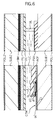
- Figure 2 shows a cross section taken along the line 3-3 of Figure 1.
- Figure 3 shows a cross section of a thin-film transistor TFT taken along the line 4-4 of Figure 1.
- Figure 4 shows a cross section of a storage capacitor Cstg taken along the line 5-5 of Figure 1.
- a lower transparent glass substrate SUB1 On the lower transparent glass substrate SUB1 are formed a thin-film transistor TFT, a storage capacitor Cstg and other electrodes.
- On the upper transparent glass substrate SUB2 are formed a color filter FIL and a black matrix pattern BM for light shielding.
- each of the transparent glass substrates SUB1, SUB2 On the inner side (liquid crystal LC side) of each of the transparent glass substrates SUB1, SUB2, alignment or orientation films ORI1, ORI2 are formed that control the initial orientation of the liquid crystal.
- polarizors On the outer side of each of the transparent glass substrates SUB1, SUB2 are placed polarizors whose polarizing axes are crossed perpendicularly (crossed-Nicols arrangement).
- the thin-film transistor TFT operates in such a way that its channel resistance between the source and the drain decreases when a positive bias is applied to the gate electrode GT and, when the bias is set to zero, increases.
- the thin-film transistor TFT has an i-type (intrinsic, meaning no conductivity type determining impurities are introduced) semiconductor layer AS comprising a gate electrode GT, a gate insulating film GI and an i-type amorphous silicon (Si), a pair of source electrodes SD1 and a pair of drain electrodes SD2.
- the source and the drain are determined essentially by the bias polarity between them, and in the circuit of this liquid crystal display device the bias polarity is reversed during operation and thus it should be understood that the source and the drain switch to each other during the operation. In the following description, however, one of them is fixedly as a source and the other a drain for convenience.
- the gate electrode GT is formed continuously with the scanning signal line GL so that a part of the scanning signal line GL forms the gate electrode GT.
- the gate electrode GT is a part extending beyond an active region of the thin-film transistor TFT and is formed slightly larger than the i-type semiconductor layer AS so as to completely cover it (when viewed from below).
- the gate electrode GT serves to protect the i-type semiconductor layer AS from external light and backlight.
- the gate electrode GT is formed of a single layer of a conductive film g1.
- the conductive film g1 may be an aluminum (Al) film formed by sputtering. Over the conductive film g1 is formed an anodic oxide film AOF of aluminum.
- the scanning signal line GL is formed of the conductive film g1.
- the conductive film g1 of this scanning signal line GL is made by the same manufacture process as the conductive film g1 of the gate electrode GT and formed integrally with it.
- a gate voltage Vg is supplied from an external circuit to the gate electrode GT.
- the anodic oxide film AOF of aluminum is also formed over the scanning signal line GL.
- the part of the scanning signal line GL that crosses the video signal lines DL is formed narrow to reduce the probability of short-circuit with the video signal lines DL and is bifurcated so as to be cut by laser trimming even when a short-circuit occurs.
- the counter electrode CT is formed of a conductive film g1 that is in the same layer as the gate electrode GT and the scanning signal line GL.
- the aluminum anodic oxide film AOF is formed over the counter electrode CT, too.
- the counter electrode CT is applied with a counter voltage Vcom.
- the counter voltage Vcom is set at a potential which is, by the field-through voltage ⁇ Vs lower than an intermediate DC potential between a minimum level drive voltage Vdmin and a maximum level drive voltage Vdmax applied to the video signal lines DL, the field-through voltage ⁇ Vs being generated when the thin-film transistor TFT is turned off.
- an AC voltage needs to be applied.
- the counter voltage line CL is formed of a conductive film g1.
- the conductive film g1 of the counter voltage line CL is deposited in the same manufacturing process for the conductive film g1 of the gate electrode GT, the scanning signal line GL and the counter electrode CT, and is formed integrally with the counter electrode CT. Through this counter voltage line CL the counter voltage Vcom is supplied from the external circuit to the counter electrode CT.
- the aluminum anodic oxide film AOF is also formed over the counter voltage line CL.
- the part of the counter voltage line CL that crosses the video signal lines DL is, like the scanning signal line GL, formed narrow to reduce the probability of short-circuit with the video signal lines DL and is bifurcated so as to be cut by laser trimming even when a short-circuit occurs.
- the insulating film GI is used as a gate insulating film to apply an electric field to the semiconductor layer AS as well as the gate electrode GT.
- the insulating film GI is formed over the gate electrode GT and the scanning signal line GL.
- the insulating film GI may be a silicon nitride film deposited to a thickness of 1200-2700 angstrom (A) (in this embodiment, about 2400 A) by, for instance, a plasma chemical vapor deposition.
- the gate insulating film GI is formed so as to enclose the whole matrix area AR, with its peripheral portion removed to expose external connection terminals DTM, GTM.
- the insulating film GI serves also as electric insulation between the scanning signal line GL or counter voltage line CL and the video signal lines DL.
- the i-type semiconductor layer AS is made of amorphous silicon and deposited to a thickness of 200-2200 A (in this embodiment, about 2000 A).
- a layer d0 is an N(+) amorphous silicon semiconductor layer doped with phosphorus (P) for ohmic contact, and is left only where there is an i-type semiconductor layer AS below and a conductive layer d1 (d2) above.
- the i-type semiconductor layer AS is also provided between the scanning signal line GL or counter voltage line CL and the video signal lines DL at their intersections (crossover portions).
- the i-type semiconductor layer AS at the crossover portions reduces the possibility of short-circuit between the scanning signal line GL or counter voltage line CL and the video signal lines DL.
- the source electrode SD1 and the drain electrode SD2 are each formed of a conductive film d1 in contact with the N(+) semiconductor layer d0 and a conductive film d2 formed over the first conductive film d1.
- the conductive film d1 is made of chromium (Cr) by sputtering to a thickness of 500-1000 A (in this embodiment, about 600 A).
- the Cr film has an increased stress when formed to a greater thickness and therefore its thickness is limited to about 2000 A at most.
- the Cr film is used (as a so-called barrier layer) to ensure a satisfactory adhesion with the N(+) semiconductor layer d0 and to prevent aluminum of the conductive film d2 from diffusing into the N(+) semiconductor layer d0.
- the conductive film d1 may be a high melting point metal (Mo, Ti, Ta, W) film or a high melting point silicide (MoSi 2 , TiSi 2 , TaSi 2 , WSi 2 ) film.
- the conductive film d2 is formed by sputtering aluminum to a thickness of 3000-5000 A (in this embodiment, about 4000 A).
- the aluminum film has smaller stresses than the Cr film and can be formed to a greater thickness, thus reducing the resistances of the source electrodes SD1, drain electrodes SD2 and video signal lines DL. Improving the step coverage, and ensuring the extension over the steps formed due to the formation of the gate electrode GT and i-type semiconductor layer AS.
- the conductive film d1 and conductive film d2 are patterned with the same mask pattern and then, by using the same mask or by using the conductive film d1 and conductive film d2 as masks, the N(+) semiconductor layer d0 is removed. That is, the N(+) semiconductor layer d0 remaining on the i-type semiconductor layer AS is removed in a self-alignment manner in the portions other than the conductive film d1 and conductive film d2. At this time, because the N(+) semiconductor layer d0 is etched away to its full thickness, the i-type semiconductor layer AS is also etched slightly at the surface. The degree of the etching can be controlled by the etching time.
- the video signal lines DL are formed of a source electrode SD1, a second conductive film in the same layer as the source electrode SD1, and a third conductive film d3.
- the video signal lines DL are formed integrally with the drain electrode SD2.
- the pixel electrode PX is formed of a source electrode SD1, a second conductive film in the same layer as the source electrode SD1, and a third conductive film d3.
- the pixel electrode PX are formed integrally with the source electrode SD1.
- the pixel electrode PX is so formed as to overlap with the counter voltage line CL.
- This overlapping forms a storage capacitor (a capacitive device) Cstg having the pixel electrode PX as one electrode PL2 and the counter voltage line CL as another electrode PL1.
- the dielectric film of the storage capacitor Cstg is formed of the insulating film GI used as a gate insulating film of the thin-film transistor TFT and the anodic oxide film AOF.
- the storage capacitor Cstg is formed in a region where the width of the conductive film g1 of the counter voltage line CL is enlarged.
- a passivation layer PSV1 Over the thin-film transistor TFT is formed a passivation layer PSV1, which has a primary function of protecting the thin-film transistor TFT against moisture and is made of a highly transparent and moisture-resistant material.
- the passivation layer PSV1 may be formed of a silicon oxide layer or silicon nitride layer deposited by a plasma CVD device to a thickness of about 1 ⁇ m.
- the passivation layer PSV1 is formed to enclose the entire matrix area AR with its peripheral portion removed to expose the external connection terminals DTM, GTM.
- the thickness of the passivation layer PSV1 and the gate insulating film GI the former is made thick for the protection effect and the latter is made thin considering the mutual conductance gm of a transistor.
- the passivation layer PSV1 with a high protecting capability is formed larger than the gate insulating film GI to protect as wide an area as possible at the peripheral portion as well.
- a light shielding film BM (generally called a black matrix) that prevents transmitted light passing through unwanted gaps (other than the gaps between the pixel electrode PX and the counter electrode CT) from going toward the display surface and degrading the contrast.
- the light shielding film BM also serves to prevent external light or backlight from entering the i-type semiconductor layer AS. That is, the i-type semiconductor layer AS of the thin-film transistor TFT is sandwiched by the upper and lower light shielding films BM and the slightly large gate electrode GT, and thus protected against external natural light and backlight.
- a closed polygonal contour line of the light shielding film BM shown in Figure 1 represents an aperture inside of which the light shielding film BM is not formed.
- This contour line pattern is just one example.
- the boundary line in the vertical direction of the figure is determined according to the precision of alignment between the upper and lower substrates. When the alignment precision is better than the width of the counter electrode CT adjoining the video signal lines DL, setting the contour line within the width of the counter electrode allows the aperture to be enlarged.
- the light shielding film BM is made of a film that has a light shielding capability and a high insulating capability not to influence the electric field between the pixel electrode PX and the counter electrode CT.
- the light shielding film BM is made of a resist material mixed with black pigment and formed to a thickness of about 1.2 ⁇ m.
- the light shielding film BM is formed as a grid around each pixel to define an effective display area of each pixel.
- the contour of each pixel is made clear by the light shielding film BM. That is, the light shielding film BM has two functions, one as a black matrix and one as a light shielding means for the i-type semiconductor layer AS.
- the light shielding film BM is also formed at the peripheral portion like a frame and its pattern is continuous with the pattern of the matrix area of Figure 1 having a plurality of dotlike openings.
- the light shielding film BM at the peripheral portion extends to the outside of the seal portion SL to prevent light such as reflected light produced in the apparatus equipped with the liquid display device, such as a personal computer from entering the matrix area.
- the light shielding film BM is kept about 0.3-1.0 mm inside from the edge of the substrate SUB2, avoiding the cut area of the substrate SUB2.
- the color filter FIL comprises alternated red, green and blue stripe filters formed at portions facing the pixels.
- the color filter FIL overlaps the edge portion of the light shielding film BM.
- the color filter FIL can be formed as follows. First, on the surface of the upper transparent glass substrate SUB2 a dyeing base made of such a material as acrylic resin is formed and then removed in areas other than the red filter forming area by photolithography. Then, the dyeing base is colored with a red dye and fixed to form a red filter R. This is followed by the similar process to form a green filter G and a blue filter B.
- the overcoating film OC is provided to prevent leakage of the dye of the color filter FIL into the liquid crystal LC and to planarize stepped portions formed by the color filter FIL and the light shielding film BM.
- the overcoating film OC may be made of a transparent resin material such as acrylic resin or epoxy resin.
- the liquid crystal material is a nematic liquid crystal with a positive dielectric anisotropy ⁇ of 10.2 and a refractive index anisotropy ⁇ n of 0.084 (589 nm at 20°C).
- the liquid crystal layer has a thickness of 5.0 ⁇ m and a retardation ⁇ n ⁇ d of 0.42 ⁇ m. With this retardation ⁇ n ⁇ d, it is possible to obtain the maximum contrast for the initial orientation angle and polarizer arrangement described later. That is, in Embodiment 1, the retardation ⁇ n ⁇ d is so determined as to produce a display of 0-th order birefringence (first minimum) mode.
- the thickness of the liquid crystal layer is controlled by polymer beads.
- the liquid crystal material LC is not particularly limited. It is noted, however, that the larger the dielectric anisotropy ⁇ and the smaller the elastic constant K2 associated with twisting, the lower the drive voltage can be.
- the time taken to inject the liquid crystal can be reduced and variation in the gap between the substrates also can be reduced.
- the thickness is 8 ⁇ m or less; desirably, to obtain the response speed of around 30 ms the liquid crystal layer thickness should preferably be 5 ⁇ m or less.
- the orientation film is made of polyimide.
- the orientation film ORI1 on the lower substrate side is rubbed in a rubbing direction RDR1 and the orientation film ORI2 on the upper substrate side is rubbed in a rubbing direction RDR2.
- the initial orientation angle is defined to be positive for a counterclockwise rotation with respect to the in-plane direction of the lateral electric field and to range from -90 degrees to 90 degrees. That is, either in the rubbing direction RDR or in the opposite direction, the initial orientation direction is in the range from -90 degrees to 90 degrees with respect to the in-plane direction of the lateral electric field.
- the initial orientation angle ⁇ 1 between the rubbing direction RDR1 and the applied electric field direction EDR on the orientation film ORI1 side is set at -45 degrees.
- the initial orientation angle ⁇ 2 between the rubbing direction RDR2 and the applied electric field direction EDR on the orientation film ORI2 side is set at 45 degrees.
- ⁇ 1 and ⁇ 2 it is important to set ⁇ 1 and ⁇ 2 so that they may fall in the range from -90 degrees to -35 degrees and in the range from 35 degrees to 90 degrees, or preferably set at -45 degrees and 45 degrees respectively.
- the orientation of the tilt angle of liquid crystal molecules in the liquid crystal layer at the upper and lower substrate interface is in the "splay" state that the liquid crystal molecules produce an effect of compensating for optical characteristics to provide a wide viewing angle characteristic.
- the response speed of this invention can also be increased by setting the initial orientation angles ⁇ 1, ⁇ 2 so that the tilt angle of the liquid crystal molecules in the liquid crystal layer is in the "parallel" state.
- the rubbing direction RDR1 is, for example, -45 degrees ( ⁇ 1 is -45 degrees) with respect to the in-plane direction of the lateral electric field and the rubbing direction RDR2 is -135 degrees ( ⁇ 2 is 45 degrees) with respect to the in-plane direction of the lateral electric field.
- a polarizer of Nitto Denko make, G1220DU, is used, and the polarizing axis MAX1 of the polarizer POL1 on the lower substrate side is aligned with the direction of electric field EDR.
- the angle ⁇ 1 between the polarizing axis MAX1 of the polarizer POL1 and the applied electric field direction EDR is set to 0 degree.
- the polarizing axis MAX2 of the upper polarizer POL2 is set perpendicular to the polarizing axis MAX1 of the lower polarizer POL1. That is, the angle ⁇ 2 between the polarizing axis MAX2 of the upper polarizer POL2 and the applied electric field direction EDR is set to 90 degrees.
- the angle between the polarizing axis MAX1 and the polarizing axis MAX2, ⁇
- , is set to 90 degrees.
- Figure 16 shows this relationship.
- Figure 5 is a plan view showing an essential peripheral portion around the matrix (AR) of the display panel PNL including the upper and lower glass substrates SUB1, SUB2.
- Figure 6 shows on the left a cross section of an external connection terminal GTM region to which the scanning circuit is to be connected, and on the right a cross section of a seal portion with no external connection terminals.
- this panel In the manufacture of this panel, if the panel size is small, a plurality of devices are fabricated simultaneously from a single glass substrate and then divided into individual panels for improved throughput. If the panel size is large, a standard size glass substrate is commonly used to fabricate any type kind of device in order to share the manufacturing facility and then cut to an appropriate size for each kind of device. In either case, after being subjected to a predetermined sequence of processes, the glass substrate is cut.
- Figure 5 and 6 represent the latter case. Both of these figures show the state of the upper and lower substrates SUB1, SUB2 after being cut., LN denoting the edge of the substrates before cutting.
- the size of the upper substrate SUB2 in a finished state is limited to the inside of the lower substrate SUB1 to expose these terminals.
- the terminal groups Tg, Td including the scanning circuit connection terminals GTM, the signal electrode circuit connection terminals DTM, and their lead out wiring portion are named in groups of terminals grouped for each tape carrier package TCP ( Figure 13, 14) mounted with an integrated circuit chip CHI.
- the leadout wiring from the matrix portion of each terminal group to the external connection terminal portion are inclined as they approach the ends.
- the counter electrode terminal COT is a terminal to apply the counter voltage from the external circuit to the counter electrode CT.
- the counter voltage lines CL of the matrix portion are led out to the opposite side of the scanning circuit terminals GTM (to the right side in the figure) are grouped together with a common bus line CB and connected to the counter electrode terminal COT.
- a seal pattern SL is formed along their edges except for a liquid crystal injection port INJ so that the liquid crystal LC can be sealed.
- the sealing material may be made of epoxy resin.
- the orientation films ORI1, ORI2 are formed inside the seal pattern SL.
- the polarizers POL1, POL2 are formed on the outer surfaces of the lower transparent glass substrate SUB1 and the upper transparent glass substrate SUB2, respectively.
- the liquid crystal LC is sealed in a space enclosed by the lower orientation film ORI1 and upper orientation film ORI2, both setting the orientation of the liquid crystal molecules, and by the seal pattern SL.
- the lower orientation film ORI1 is formed over the passivation layer PSV1 on the lower transparent glass substrate SUB1 side.
- This liquid crystal display device is assembled by stacking a variety of layers on the lower transparent glass substrate SUB1 and on the upper transparent glass substrate SUB2, separately; forming the seal pattern SL on the upper transparent glass substrate SUB2 side; stacking the lower transparent glass substrate SUB1 and the upper transparent glass substrate SUB2; injecting the liquid crystal LC from the injection port INJ of the seal material SL; sealing the injection port INJ with epoxy resin or the like; and cutting the upper and lower substrates.
- Figure 7 shows the connection structure the scanning signal line GL of the display matrix to its external connection terminal GTM.
- Figure 7(A) is a plan view and Figure 7(B) is a cross section taken along the line B-B of (A). The figure corresponds to the lower part of the connection structure and the inclined wiring is shown by straight lines for convenience.
- AO denotes a boundary line of a photoresist direct drawing, i.e., a photoresist pattern for selective anodic oxidation.
- This photoresist is removed after anodic oxidation and thus the pattern AO shown in Figure 7 does not remain in the completed product. But because the oxide film AOF is selectively formed over the gate line GL as shown in the cross section, its trace remains.
- the left side of the photoresist boundary line AO is an area that is covered with a resist and not subjected to anodic oxidation while the right side is exposed from the resist for anodic oxidation.
- anodically-oxidized aluminum layer g1 On the anodically-oxidized aluminum layer g1 is formed an oxide, Al 2 O 3 film AOF, reducing the volume of the underlying conductive portion.
- the anodic oxidation is performed under properly controlled conditions including time and voltage so that the underlying conductive portion may remain.
- the aluminum layer g1 is shown by a hatched portion for easy recognition, and the region that is not subjected to anodic oxidation is patterned in the form of comb teeth, for the following reason.
- whiskers are formed on the surface.
- the aluminum layer is divided into a plurality of parallel narrow lines to prevent the formation of whiskers while at the same time minimizing the probability of line breakage and the reduction of conductivity.
- the gate terminal GTM comprises the aluminum layer g1 and a transparent conductive layer g2 that protects the surface of g1 and improves the reliability of connection with tape carrier packages.
- the transparent conductive layer g2 is a transparent conductive indium-tin-oxide film (ITO: NESA film) formed by sputtering to a thickness of 100-2000 A (in this embodiment, about 1400 A).
- Conductive layers d1, d2 are formed over the aluminum layer g1 and its side.
- the conductive layer d1 is a Cr layer that has good connectability with both the aluminum layer and the transparent conductive layer g2 to reduce connection resistance and thereby to compensate for detective connection between the aluminum layer and the transparent conductive layer g2.
- the conductive layer d2 remains there because it is formed by the same mask used for the conductive layer d1.
- the gate insulating film GI is formed on the right side of its boundary line and the passivation layer PSV1 is also formed on the right side of its boundary line.
- the terminal portion GTM located at the left end is exposed for electrical contact with external circuits.
- the figure shows only one pair of gate line GL and gate terminal, the actual device has a plurality of such pairs arranged parallelly in a vertical direction to form terminal groups Tg ( Figure 5).
- the left end of the gate terminal is extended beyond the cutting area of the substrate and short-circuited by a wiring Shg (not shown) during the process of manufacture.
- a shorting line SHg is used for supplying electricity during the anodic oxidation and for preventing electrostatic breakdown during the rubbing of the orientation film ORI1 in the process of manufacture.
- Figure 8 shows the connection structure from the video signal line DL to its external connection terminal DTM.
- Figure 8(A) is a plan view and Figure 8(B) is a cross section taken along the line B-B of Figure 8(A).
- Figure 8 corresponds to the upper right area of Figure 5 although the direction of the figure is changed for convenience.
- the right-hand end area of Figure 8 corresponds to the upper end portion of the substrate SUB1.
- TSTd designates a testing pad, which is formed wider than its line portion so that a probe or the like can be brought into contact with it, although it is not connected with external circuits.
- the drain terminal DTM too, is formed wider than its line portion for connection with external circuits.
- the external connection drain terminals DTM are arranged in the vertical direction, forming the terminal groups Td (subscript omitted) as shown in Figure 5 and extending beyond the cutting line of the substrate SUB1.
- the drain terminals DTM are all short-circuited by the wiring SHd (not shown) to prevent electrostatic breakdown during the manufacturing process.
- the testing pad TSTd is formed at every other video signal line DL as shown in Figure 8.
- the drain connection terminal DTM is formed of a single transparent conductive layer g2 and is connected to the video signal lines DL at portions where the gate insulating film GI is removed.
- the semiconductor layer AS formed over the end of the gate insulating film GI is to etch the edge of the gate insulating film GI in a tapered shape.
- the passivation layer PSV1 is of course removed from the terminal DTM for connection with the external circuits.
- the leadout wire from the matrix portion to the drain terminal portion DTM has its layers d1, d2-which are at the same level of the video signal lines DL-extending to an intermediate portion of the passivation layer PSV1 and connected with the transparent conductive layer g2 inside the passivation layer PSV1.
- This arrangement is intended to protect the aluminum layer d2, vulnerable to galvanic corrosion, with the passivation layer PSV1 and the seal pattern SL.
- Figure 9 shows the connection structure from the counter voltage line CL to its external connection terminal CTM.
- Figure 9(A) is a plan view and Figure 9(B) is a cross section taken along the line B-B of (A). The figure corresponds to the upper left area of Figure 5.
- the counter voltage lines CL are grouped with the common bus line CB and led out to the counter electrode terminal CTM.
- the common bus line CB comprises a conductive layer g1, and other conductive layers d1, d2 stacked on the first layer g1. This arrangement is designed to reduce the resistance of the common bus line CB and thereby supply a sufficient counter voltage from the external circuit to each counter voltage line CL. This structure is characterized by the ability to reduce the resistance of the common bus line without imposing any additional burden on the conductive layer.
- the conductive layer g1 of the common bus line CB is not subjected to anodic conversion, in order that it is electrically connected to the conductive layers d1, d2. It is also exposed from the gate insulating film GI.
- the counter electrode terminal CTM has the transparent conductive layer g2 stacked over the conductive layer g1.
- the conductive layer g1 is covered with the transparent conductive layer g2, which has good corrosion resistance, to protect the surface of the conductive layer g1 against galvanic corrosion.
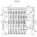
- FIG. 10 An equivalent circuit of the display matrix portion and its peripheral circuit are shown in Figure 10.
- AR represents a matrix array in which a plurality of pixels are arranged in two dimensional array.
- X represents the video signal lines DL, with subscripts G, B and R representing green, blue and red pixels.
- Y means scanning signal lines GL, with subscripts 1, 2, 3, ..., end indicating the order of scan timing.
- the scanning signal lines Y (the subscripts are omitted) are connected to a scanning circuit V and the video signal lines X (the subscripts are omitted) are connected to a video signal driving circuit H.
- a circuit SUP includes a power supply circuit for producing step-down power supply voltages from one power source and a circuit for converting information for CRT from a host computer (higher order computer) into information for a TFT liquid crystal display.
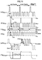
- Figure 11 shows drive signal waveforms for the liquid crystal display device of this invention.
- the counter voltage is transformed into alternating rectangular waves having binary values, Vch and Vcl, and in synchronism with the alternating waves a nonselection voltage for the scanning signals Vg (i-1), Vg(i) is changed between two values, Vh1h and Vg1l, in each scanning period.
- the amplitude of the counter voltage and the amplitude of the nonselection voltage are set equal.
- the video signal voltage is obtained by subtrating half the counter voltage from the voltage to be applied to the liquid crystal layer.
- the counter voltage may be a DC voltage but transforming it into the AC voltage makes it possible to reduce the maximum amplitude of the video signal voltage, allowing the use of a video signal driving circuit (signal side driver) with a lower dielectric strength.
- the storage capacitor Cstg is provided for holding the video information written in a pixel for a long period (after the thin-film transistor TFT is turned off).
- the storage capacitor Cstg cannot hold the video information in the pixel.
- the storage capacitor Cstg is an essential constitutional element.
- the storage capacitor Cstg when the thin-film transistor TFT is switched, also works to reduce the effect of the gate potential change ⁇ Vg on the pixel electrode potential Vs. This is expressed by the following equation.
- ⁇ Vs ⁇ Cgs/(Cgs + Cstg + Cpix) ⁇ x ⁇ Vg
- Cgs is a parasitic capacitance produced between the gate electrode GT and the source electrode SD1 of the thin-film transistor TFT
- Cpix is a capacitance produced between the pixel electrode PX and the counter electrode CT
- ⁇ Vs is a voltage generally called a feed-through voltage
- This change ⁇ Vs is a cause of a DC component applied to the liquid crystal LC and can be reduced by increasing the storage capacitor Cstg.
- Reduced DC components applied to the liquid crystal LC improve the service life of the liquid crystal LC, mitigating so-called image persistence, a phenomenon in which a previous image remains when the liquid crystal screen is switched to another image.
- the gate electrode GT is so formed large as to cover the entire i-type semiconductor layer AS, the overlapping area with the source electrode SD1 and the drain electrode SD2 correspondingly increase, which in turn increases the parasitic capacitance Cgs, making the pixel electrode potential Vs more susceptible to the influences of the gate (scanning) signal Vg.
- the provision of the storage capacitor Cstg can eliminate this demerit.
- the method of driving is not limited to the above and other active matrix driving methods may be employed. These methods all fall in the scope of this invention.
- Figure 12 is a plan view showing the display panel PNL of Figure 5 connected with the video signal driving circuit H and the scanning circuit V.
- CHI represents drive IC chips to drive the display panel PNL (five shown at the bottom are drive IC chips on the scanning circuit side; ten shown to the left are drive chips on the video signal driving circuit side).
- TCP denotes tape carrier packages mounted with the drive IC chips CHI by the tape automated bonding (TAB) as described later referring to Figure 13 and 14.
- a printed circuit board PCB1 is mounted with the TCPs and capacitors and is divided in two, one for the video signal driving circuit and the other for the scan signal driving circuit.
- FGP denotes a frame ground pad to which are soldered springlike pieces formed by cutting a shield case SHD.
- a flat cable FC electrically connects the lower-side printed circuit board PCB1 and the left printed circuit board PCB1.
- the flat cable FC may, as shown, be formed by sandwiching a plurality of lead wires (of phosphor bronze plated with Sn) between a striped polyethylene layer and a polyvinyl alcohol layer.
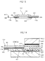
- Figure 13 shows a cross-sectional structure of the tape carrier package TCP where the IC chips CHI comprising the scan signal driving circuit V and the video signal driving circuit H is mounted on the flexible printed circuit boards.
- Figure 14 is a cross section showing an essential part of the liquid crystal display panel connected to the scan signal terminal GTM.
- TTB denotes an input terminal/wiring portion of the IC circuit CHI.
- TTM represents an output terminal/wiring portion of the IC circuit CHI. These are made, for instance, of Cu and their inner ends (generally called inner leads) are connected with bonding pads PAD of the IC circuit CHI by the facedown bonding.
- the outer ends (generally called outer leads) of the terminals TTB, TTM correspond to the input and output, respectively, of the semiconductor IC circuit chip CHI and are connected to the CRT/TFT conversion circuit/power supply circuit SUP by soldering and to the liquid crystal display panel PNL through the anisotropic conductive film ACF.
- the package TCP is connected to the panel so that the package end covers the edge of the passivation layer PSV1 that exposes the connection terminal GTM on the panel PNL side.
- the outer connection terminal GTM (DTM) is covered with at least one of the passivation layer PSV1 and the package TCP, so that its resistance against galvanic corrosion is enhanced.
- BF1 denotes a base film made, for example, of polyimide.
- SRS is a solder resist film as a mask to prevent solder from flowing to unwanted areas during the soldering process.
- the gap between the upper and lower glass substrates on the outer side of the seal pattern SL is, after cleaning, protected with epoxy resin EPX or the like.
- silicone resin SIL is placed between the package TCP and the upper substrate SUB2 for double protection.
- the printed circuit board PCB2 is mounted with electronic parts such as ICs, capacitors and resistors.
- the printed circuit board PCB2 is mounted with a circuit SUP that includes a power supply circuit for producing step-down supply voltages from a single power source and a circuit for converting CRT information from a host computer (higher order computer) into TFT liquid crystal display device information.
- CJ represents a connector portion for a connector (not shown) that is connected with an external circuit.
- the printed circuit board PCB1 and the printed circuit board PCB2 are electrically connected with a flat cable FC.
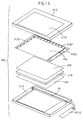
- Figure 15 is an exploded perspective view of constitutional parts of a liquid crystal display module MDL.
- SHD represents a framelike shield case (metal frame) made of a metal plate; LCW a window for the liquid crystal display; PNL a liquid crystal display panel; SPB a diffuser; LCB a light conductor; RM a reflector; BL a backlight fluorescent tube; and LCA a backlight case. These are stacked together in a vertical relationship shown in the figure to form a module MDL.
- the module MDL is secured together with claws and hooks provided to the shield case SHD.
- the backlight case LCA is so shaped as to accommodate the backlight fluorescent tube BL, diffuser SPB, light conductor LCB and reflector RM.
- the light from the backlight fluorescent tube BL arranged at the side of the light conductor LCB is diffused by the light conductor LCB, reflector RM and diffuser SPB to produce uniform light at the display surface and directed to the liquid crystal display panel PNL.
- the backlight fluorescent tube BL is connected with an inverter circuit board PCB3 which is a power source of the backlight.
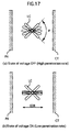
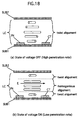
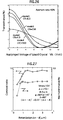
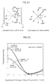
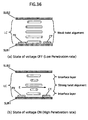
- Figure 17 and 18 show the principle of driving the liquid crystal of Embodiment 1.
- the liquid crystal molecules in the liquid crystal layer are in the initial state where they are twisted 90 degrees clockwise from the upper substrate SUB2 to the lower substrate SUB1, as shown in Figure 17(a).
- the part of the twisted liquid crystal molecules in the direction of thickness of the liquid crystal layer decreases as shown in Figure 17(b), only molecules in the region close to the interfaces with the upper remain twisted and lower substrates and a major part of the liquid crystal molecules is oriented homogeneously in the voltage application direction.
- the liquid crystal layers near the interfaces actually remain twisted, so that retardation does not become zero.
- the thickness of the liquid crystal layer of the twisted molecules can be reduced infinitely, making it possible to assume that almost all molecules can be homogeneously oriented. Because the polarizers are cross-Nicols-arranged (perpendicularly to each other), light cannot pass through, producing a black display if there is no birefringence.
- Embodiment 1 With the configuration of Embodiment 1 the normally open type electro-optical characteristic is obtained that enables white display when no voltage is applied.
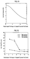
- the transmittance at the time of white display was 4.5%. Further, the contrast ratio of 3 was obtained at the time of black display by applying a drive voltage of 12 V.
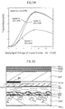
- Figure 19 shows an applied voltage-transmittance characteristic of Embodiment 1.
- Embodiment 1 increasing the drive voltage causes the transmittance to decrease, thus improving the contrast ratio. Because of the limitation on the withstand voltage of the drive circuit, however, in this embodiment, the maximum drive voltage is 12 V. It should be noted that the present invention also includes cases where higher or lower maximum drive voltages are used for the driving.
- the response speed of the liquid crystal display device of Embodiment 1 was 22 ms, of which 8 ms was a rise time and 14 ms a fall time.
- Figure 20 to 22 show the rise time Tr, the fall time and the response speed.
- Embodiment 1 The response speed of Embodiment 1 is shorter than 30 ms, enabling display of a dynamic image, and this means that a dynamic image can be displayed in good condition without any trailing.
- Figure 20 to 22 show, for comparison, the response speed, of the first case (conventional configuration 1) and the second case (conventional configuration 2) described above.
- the response speed of this invention is about 1/2 to 1/4 that of the conventional configurations, realizing a significant improvement.
- the conventional configuration 2 had a liquid crystal layer thickness of 4.0 ⁇ m when its response speed was measured.
- the conventional configuration 2 has a normally closed (normally black) characteristic that enables white display when applied with a voltage
- the liquid crystal layer thickness was 4.0 ⁇ m in order to make the transmittance of the same liquid crystal material for a white display equal to that of the conventional configuration 1 and the Embodiment 1.
- the conventional configuration 1 and Embodiment 1 were set at 5.0 ⁇ m in the liquid crystal layer thickness.
- this invention produces no trailing image, a drawback that occurs particularly when a dynamic image is displayed in a half-tone mode.
- the viewing angle characteristic of this invention was more than 140 degrees in the vertical and horizontal directions, which compares favorably with those of the conventional configuration 1 and 2. Further, the color tone variation and the gradation inversion recognized when viewed at a particular angle, which are the probrems of the conventional configuration 2, were mitigated.
- the coler tone variation is a phenomenon that, assuming the direction of an in-plane component of the lateral electric field to be 0 degree, the region along the direction of about 45 degrees and 225 degrees, for example, changes its color from white to yellow (or blue) and the area along the direction of about -45 degrees and 135 degrees changes to blue (or yellow).
- the gradation inversion is a phenomenon that, when viewed at an obliqe angle, white changes to yellow or blue. These phenomena occur because when white is displayed, a change in retardation due to inclination of the viewing angle causes the liquid crystal layer near the upper substrate and the liquid crystal layer near the lower substrate to compensate for each other.
- this invention provides the response speed of less than 30 ms, the minimum requirement for displaying a dynamic image.
- An additional advantage is a further improvement of the viewing angle, compared to the conventional configuration. Because a material with greater refractive index anisotropy ⁇ n than that of the conventional configuration 2 can be used, a wider range of materials becomes available. Further, because the thickness of the liquid crystal layer can be set larger, the gap between the substrates is more easily made uniform, improving the uniform distribution of brightness. The thicker liquid crystal layer contributes to a shorter liquid crystal injection time.
- the cross-sectional structure of the thin-film transistor TFT and the electrode arrangement shown in Embodiment 1 are just one example and it is possible to use another TFT structure and electrode arrangement (including one in which the counter electrodes are placed on the color filter substrate) in this invention.
- Embodiment 2 to Embodiment 5 are examples configuration with normally open display characteristics and optical compensation cells. They are similar in configuration to Embodiment 1 except for the following.
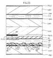
- FIG. 23 A cross-sectional structure of Embodiment 2 to Embodiment 5 is shown in Figure 23.
- the structure includes drive liquid crystal cells having drive electrodes CT, PX and thin-film transistors TFT, and optical compensation liquid crystal cells with no electrodes.
- Embodiment 2 has a configuration such that only the optical compensation liquid crystal cells added to Embodiment 1.
- Embodiment 3 has a configuration similar to that of Embodiment 2 with an increased refractive index anisotropy ⁇ n of the liquid crystal material of the drive liquid crystal cells.
- Embodiment 4 has a configuration similar to that of Embodiment 2 with the polarizing axis of the polarizer optimized.
- Embodiment 5 has a configuration in which the initial twist angle ⁇ of the drive liquid crystal cells is optimized.
- the initial twist angle ⁇ , initial orientation angles ⁇ 1, ⁇ 2, thickness of the liquid crystal layer, dielectric anisotropy ⁇ of the liquid crystal material, and refractive index anisotropy ⁇ n, all of Embodiment 2 to Embodiment 5, are shown in Table 1.
- the optical compensation liquid crystal cells comprise, as shown in Figure 23, a lower substrate SUB3, an upper substrate SUB4, a liquid crystal composition CLC held between these substrates, an orientation film ORI3 on the lower substrate SUB3 side, and an orientation film ORI4 on the upper substrate SUB4 side.
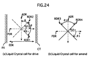
- Figure 24 shows the rubbing direction of the drive liquid crystal cells, the initial orientation angle and the polarizing axis of polarizer, and the rubbing direction of the optical compensation liquid crystal layer (orientation direction near the orientation film).
- the orientation film ORI3 is rubbed in the RDR3 direction
- the orientation film ORI4 is rubbed in the RDR4 direction.
- ⁇ 3 is the initial orientation angle between the rubbing direction RDR3 and the applied electric field direction EDR of the drive liquid crystal cell
- ⁇ 4 is the initial orientation angle between the rubbing direction RDR4 and the applied electric field direction EDR of the drive liquid crystal cell.
- the twist angle ⁇ 2 is a twist angle of the optical compensation liquid crystal layer.
- the retardation ( ⁇ n ⁇ d)' of the optical compensation liquid crystal layer, the twist angle ⁇ 2, and the initial orientation angles ⁇ 3, ⁇ 4 are shown in Table 1.
- films holding cholesteric liquid crystal therebetween which have an optical characteristic identical to that of the optical compensation cells of Embodiment 2 to 5 may be used.
- the direction of the polarizing axis of the polarizer POL1 on the backlight input side is denoted by PDR and the direction of the polarizing axis of the polarizer POL2 on the output side is denoted by ADR.
- the liquid crystal molecules are oriented in a state shown in Figure 25(b) by applying a voltage to enable black display. That is, the liquid crystal cells of Embodiment 2 to 5 have their liquid crystal molecules near the interface strongly twisted and the liquid crystal molecules in the central portion weakly twisted.
- the phrase "weakly twisted” means a state that the ratio, twist angle/layer thickness, is small and the phrase "strongly twisted” means a state that the ratio twist angle/layer thickness, is large.
- the contrast ratio, the drive voltage and the maximum transmittance are improved progressively roughly in order of the embodiment numbers.
- the contrast ratio of 100 or higher and the maximum transmittance (absolute transmittance of the panel during a white display) of 4.1% are obtained for the drive voltage of 7 V.
- Figure 27 shows the relation between the retardation of drive cell, the contrast ratio, and the maximum transmittance.
- Figure 27 shows that the optimum retardation needs to be 750 nm or higher to produce a sufficient transmittance, preferably 1250 nm or higher that produces a sufficient contrast ratio.
- the optimal relation ⁇
- of the polarizing axis of the polarizer needs to be 90 degrees to 120 degrees, preferably 95 degrees to 115 degrees.
- Figure 29 shows the relation between the initial twist angle of the drive liquid crystal cells, the contrast ratio and the maximum transmittance.
- the initial twist angle is preferably set in a range between 90 degrees and 115 degrees to realize a sufficient contrast ratio and the maximum transmittance at the same time.
- Embodiment 6 to 8 are examples of normally closed configuration with the optical compensation cells and similar to those of Embodiment 2 to 5, except for the following.
- Embodiment 6 to 8 are similar to those of Embodiment 2 to 5 and shown in Figure 23.
- Embodiment 6 to 8 have drive liquid crystal cells with drive electrodes CT, PX and thin-film transistors TFT, and optical compensation liquid crystal cells without electrodes.
- Embodiment 6 unlike Embodiment 2, matches the retardation ( ⁇ n ⁇ d)' of the optical compensation liquid crystal cell with the retardation ( ⁇ n ⁇ d) of the drive cell.
- Embodiment 7 has a configuration in which the refractive index anisotropy ⁇ n of the liquid crystal material of the drive liquid crystal cell is set large and the retardation ( ⁇ n ⁇ d)' of the optical compensation liquid crystal cell is matched with the retardation ( ⁇ n ⁇ d) of the drive cell.
- Embodiment 8 has a configuration in which the initial twist angle ⁇ of Embodiment 7 is changed.
- the initial twist angle ⁇ , initial orientation angles ⁇ 1, ⁇ 2, thickness of the liquid crystal layer, and ⁇ and ⁇ n of the liquid crystal material, all used in Embodiment 6 to 8, are shown in Table 2.
- the retardation ( ⁇ n ⁇ d)', twist angle ⁇ 2, and the initial orientation angles ⁇ 3, ⁇ 4 of the optical compensation liquid crystal layer used in Embodiment 6 to 8 are shown in Table 2. Definitions of these parameters are the same as those of Embodiment 2 to 5.
- the optical compensation liquid crystal cells may use films holding cholesteric liquid crystal therebetween which have an optical characteristic identical to that of the optical compensation cells of the previous embodiments.
- Embodiment 6 to 8 also have the retardation ( ⁇ n ⁇ d)' of the optical compensation liquid crystal cell matched with the retardation ( ⁇ n ⁇ d) of the drive liquid crystal cell. Hence, a normally closed characteristic that the transmittance increases with the voltage applied to the liquid crystal is obtained.
- Figure 30 shows the relation between the drive voltage V1c and the transmittance T Embodiment 6 to 8.
- Embodiment 6 to 8 enables a black display (low transmission state) when no voltage is applied.
- the liquid crystal molecules are oriented in an ideally twisted state making the optical compensation by the optical compensation cell easy.
- an ideal black level i.e., the transmittance infinitely close to zero, can be achieved. It is therefore possible to widen the margin for variations in the manufacturing process, particularly the variations of the gap between substrates, allowing the stable manufacture of high-contrast products.
- Embodiment 7 enabled a contrast ratio of 100 or higher and a maximum transmittance (absolute transmittance of the panel during white display) of 4.5% for a drive voltage of 7 V.
- the response speed characteristics in Embodiment 6 and 7 are comparable to those of Embodiment 1.
- Embodiment 6 As to the relation among the retardation, contrast ratio and maximum transmittance of the drive cells, comparison between Embodiment 6 and Embodiment 7 shows that the maximum transmittance is improved in Embodiment 7 over Embodiment 6. Therefore, it is desired that the optimum retardation be set higher than 750 nm as in Embodiment 2 to 5.
- the polarizer arrangement ⁇
- is preferably set close to 90 degrees.
- Embodiment 8 by increasing the initial twist angle to more than 90 degrees it is possible to change a liquid crystal applied voltage at which the transmittance starts to increase, i.e., a threshold voltage. Hence, the voltage amplitude contributing to the display and ranging from the threshold voltage to a voltage for the maximum transmittance can be reduced. This in turn reduces the signal output range of the video signal driving circuit. In other words, the video signal driving circuit, particularly the signal driver, can be reduced in circuit size.
- the response speed is slightly slower, that is, the rise time is 12 ms, the fall time is 20 ms and the response time of 32 ms.
- the initial twist angle therefore contributes to changing the drive voltage that brings about the maximum transmittance, and it is preferably set in a range from 70 degrees to 160 degrees.
- Embodiment 9 to 13 have a normally open configuration with a uniaxial phase film and is similar to the configuration of Embodiment 1, except for the following.
- FIG. 31 A cross-sectional structure of Embodiment 9 to 13 is shown in Figure 31.
- uniaxial phase films FILM1 and FILM2 are arranged on the outer sides of the substrates SUB1, SUB2 so as to hold them therebetween.
- Embodiment 9 has the configuration such that the uniaxial phase film FILM1 and FILM2 is added to Embodiment 1.
- Embodiment 10 has the configuration such that the lagging axis of the phase film of Embodiment 9 is changed.
- Embodiment 11 has the configuration such that the retardation of the phase films of Embodiment 10 is differentiated between the upper and lower films.
- Embodiment 12 has the configuration such that the refractive index anisotropy ⁇ n of the liquid crystal material of Embodiment 11 is increased.
- Embodiment 13 has a structure where the initial twist angle of Embodiment 12 is changed.
- ⁇ 1 represents an angle between the lagging axis LDR1 of the lower phase film FILM1 and the direction of electric field EDR
- ⁇ 2 represents an angle between the lagging axis LDR2 of the upper phase film FILM2 and the direction of electric field EDR. Both of these angles are defined as positive for a counterclockwise rotation with respect to the direction of electric field EDR.
- Embodiment 9 to 13 The principle of driving the liquid crystal used in Embodiment 9 to 13 is identical with that of Embodiment 2 to 5.
- Embodiment 9 to 13 orientate the liquid crystal in a state shown in Figure 25(b), enabling black display.
- the liquid crystal cells in Embodiment 9 to 13 assume a transitional state that the liquid crystal molecules near the interface are strongly twisted while those in the central portion are weakly twisted.
- the phase films and the polarizers in such a way as to compensate for this orientation state, it is possible to achive a high contrast ratio with a low voltage.
- Embodiment 9 to 13 have response speed characteristics comparable to those of Embodiment 1.
- Figure 33 shows the relation between the drive voltage V1c and the transmittance T. It is seen that the contrast ratio and the maximum transmittance are improved progressively roughly in order of the embodiment number.
- the contrast ratio of 100 or higher and the maximum transmittance (the absolute transmittance of the panel during white display) of 4.4% are obtained for the drive voltage of 7 V.
- Embodiment 9 there is no characteristic change between Embodiment 9 and Embodiment 10. This suggests that the lagging axis angles ⁇ 1, ⁇ 2 of phase plates and the retardations ( ⁇ n ⁇ d)1, ( ⁇ n ⁇ d)2 of the phase plate do not change their characteristics if ⁇ 1 ⁇ ( ⁇ n ⁇ d)1 and ⁇ 2 ⁇ ( ⁇ n ⁇ d)2 are constant even when their values are changed.
- the optimum retardation needs to be set higher than 750 nm for a sufficient transmittance, preferably more than 1250 nm to obtain a sufficient contrast ratio.
- the relation ⁇
- of optimum polarizing axes of the polarizers needs to be set in a range of between 90 degrees and 120 degrees, preferably between 95 degrees and 115 degrees.
- the initial twist angle should preferably be set in a range between 90 degrees and 115 degrees to achive a satisfactory contrast ratio and a white display transmittance at the same time.
- FIG. 35 A cross-sectional structure, in which two phase films FILM1, FILM2 are arranged on the upper side only, is shown in Figure 35. Other arrangements can also bring about characteristics similar to those of these embodiments and they are within the scope of this invention.
- Embodiment 14 to 16 have a normally closed configuration with uniaxial phase films which is similar to that of Embodiment 9 to 13, except for the following.
- Embodiment 14 to 16 The cross-sectional configuration of Embodiment 14 to 16 is shown in Figure 31 and is similar to that of Embodiment 9 to 13.
- the uniaxial phase films FILM1, FILM2 are arranged on the outer sides of the substrates SUB1, SUB2 so as to hold them therebetween.
- Embodiment 14 has a configuration that matches the sum of retardations ( ⁇ n ⁇ d)1 + ( ⁇ n ⁇ d)2 of the uniaxial phase films to the retardation ( ⁇ n ⁇ d) of the drive cell.
- Embodiment 15 has a configuration in which, under the retardation condition of Embodiment 14, the dielectric anisotropy ⁇ n of the liquid crystal material of the drive liquid crystal cells is increased.
- Embodiment 16 is an example where the initial twist angle ⁇ of Embodiment 15 is changed.
- ⁇ 1 represents the angle between the lagging axis LDR1 of the lower phase film FILM1 and the direction of electric field EDR
- ⁇ 2 represents the angle between the lagging axis LDR2 of the upper phase film FILM2 and the direction of electric field EDR
- ( ⁇ n ⁇ d)1 is the retardation of the lower phase film
- ( ⁇ n ⁇ d)2 is the retardation of the upper phase film.
- Figure 32 shows their angular relationship.
- Embodiment 14 to 16 matches the sum of the retardations ( ⁇ n ⁇ d)1 + ( ⁇ n ⁇ d)2 of the uniaxial phase films to the retardation ( ⁇ n ⁇ d) of the drive liquid crystal cell so as to realize a normally closed characteristic, in which the transmittance increases with the voltage applied to the liquid crystal.
- Figure 34 shows the relation between the drive voltage V1c and the transmittance T for Embodiment 14 to 16.
- Embodiment 14 to 16 enable a black display (low transmittance state) when no voltage is applied.
- Embodiment 15 and 16 enable a contrast ratio of 100 or higher and a maximum transmittance (absolute transmittance of the panel during white display) of 4.5% for a drive voltage of 7 V.
- the response speed characteristics in Embodiment 14 and 15 are comparable to those of Embodiment 1.
- Embodiment 14 As to the relation among the retardation, the contrast ratio and the maximum transmittance of the drive cells, comparison between Embodiment 14 and Embodiment 15 shows that the maximum transmittance is improved in Embodiment 15 over Embodiment 14. Therefore, it is desired that the optimum retardation be set higher than 750 nm as in Embodiment 9 to 13.
- the polarizer arrangement ⁇
- is preferably set close to 90 degrees.
- Embodiment 16 by increasing the initial twist angle to more than 90 degrees it is possible to change a liquid crystal applied voltage at which the transmittance starts to increase, i.e., a threshold voltage. Hence, the voltage amplitude contributing to the display and ranging from the threshold voltage to a voltage for the maximum transmittance can be reduced. This in turn reduces the signal output range of the video signal driving circuit. In other words, the video signal driving circuit, particularly the signal driver used in it, can be reduced in circuit size.
- Embodiment 16 had a rise time of 12 ms, a fall time of 20 ms and a response time of 32 ms. These suggest that the initial twist angle contributes to changing the drive voltage that leads to the maximum transmittance, and it is preferably set in a range between 70 degrees and 160 degrees.
- FIG. 35 A cross-sectional structure, in which two phase films FILM1, FILM2 are arranged on the upper side only, is shown in Figure 35.
- Other arrangements can also achive characteristics similar to those of these embodiments and they are within the scope of this invention.
- Embodiment 17 to 20 are examples of a configuration using a liquid crystal material with a negative dielectric anisotropy ( ⁇ ⁇ 0). This configuration is similar to that of Embodiment 1 except for the following.
- Embodiment 17 has a configuration where a liquid crystal material with a negative dielectric anisotropy ( ⁇ ⁇ 0) is used in Embodiment 1.
- Embodiment 18 has a configuration of Embodiment 17 with the polarizing axes of the polarizers optimized.
- Embodiment 19 has a configuration of Embodiment 18 with the initial twist angle ⁇ optimized.
- Embodiment 20 has a configuration of Embodiment 19 with the retardation ⁇ n ⁇ d and the polarizing axes of the polarizers optimized.
- the initial twist angle ⁇ , initial orientation angles ⁇ 1, ⁇ 2, thickness of the liquid crystal layer and ⁇ n of the liquid crystal material used in Embodiment 17 to 20 are shown in Table 5.
- the major axes of liquid crystal molecules are reoriented in a direction perpendicular to the electric field application direction.
- the molecules assume a state that they are weakly twisted counterclockwise from the substrate SUB2 to the substrate SUB1, as shown in Figure 36(a).
- the molecules near the central part of the liquid crystal layer change to a strongly clockwise-twisted state, with the molecules in the upper and lower layers near the interfaces twisted counterclockwise.
- black display (low transmittance state) is enabled when no voltage is applied.
- the liquid crystal molecules are oriented in an ideally twisted state making the optimization by the polarizer arrangement easy.
- an ideal black level i.e., the transmittance infinitely close to zero, can be realized. It is therefore possible to widen the margin for variations in the manufacturing process, particularly the variation of the gap between substrates, allowing the stable manufacture of high-contrast products.
- Embodiment 20 has a contrast ratio of 100 or higher and a maximum transmittance (an absolute transmittance of the panel during white display) of 4.3% for a drive voltage of 8 V.
- the response speed characteristics of Embodiment 19 and 20 are slightly slower than those of Embodiment 1, that is the rise time is 20 ms, the fall time is 16 ms and the response time is 36 ms.
- Embodiment 14 As to the relation among the retardation, contrast ratio and maximum transmittance of the drive cells, comparison between Embodiment 14 and Embodiment 15 shows that the maximum transmittance is improved in Embodiment 20 over Embodiment 19. Therefore, it is desired that the optimum retardation be set higher than 750 nm as in Embodiment 2 to 5.
- the polarizer arrangement ⁇
- is preferably set close to 90 degrees.
- the response speed is slightly slower, that is, the rise time is 40 ms, the fall time is 20 ms and the response time is 60 ms. Further, by increasing the initial twist angle, it is possible to make a significant improvement on the response speed, particularly at the leading edge. That is, the greater the initial twist angle is, the faster the response speed is.
- the initial twist angle is preferably set in a range between 20 and 50 degrees.
- Embodiment 17 As to the arrangement of the polarizers, comparison between Embodiment 17 and Embodiment 18 indicates that the contrast ratio and the maximum transmittance can be improved by optimizing the polarizers from 90 degrees.
- Embodiment 17 to 20 it is also possible to enhance the contrast ratio, lower the applied voltage or produce a normally open characteristic by using the optical compensation liquid crystal layer and the phase films, as in Embodiment 2 to 16.
- the methods for achieving these objectives are also within the scope of this invention.
- Embodiment 21 is similar to that of Embodiment 1 except for the following.
- the initial orientation angle ⁇ 1 between the rubbing direction of the lower substrate RDR1 and the direction of electric field EDR is set to -50 degrees and the initial orientation angle ⁇ 2 between the rubbing direction of the upper substrate RDR2 and the direction of electric field EDR is set to 40 degrees so that the upper and lower substrates are twisted 90 degrees.
- Embodiment 21 When the liquid crystal drive electrodes (both pixel electrode PX and counter electrode CT) are formed on the lower substrate, the electric field parallel to the substrate surface (lateral electric field) is strong near the lower substrate and progressively weaker toward the upper substrate. Hence, the liquid crystal molecules near the lower substrate are more easily rotatable than those close to the upper substrate.
- the voltage required to reorientate most of the liquid crystal molecules in the liquid crystal layer in the direction of the electric field EDR in Embodiment 21 can be lower than that of Embodiment 1.
- Embodiment 1 requires a voltage of about 12 V to enable black display while Embodiment 21 needs only about 10 V to realize the same black level as Embodiment 1.
- Embodiment 21 is that, when the liquid crystal drive electrodes are arranged only on the lower substrate, the condition
- Embodiment 21 is applicable not only to Embodiment 1 but to Embodiment 2 to 20, and these configurations are within the scope of this invention.
- this invention provides an active matrix type liquid crystal display device that realizes as wide a viewing angle as a CRT and a response speed fast enough to display a dynamic image.
Landscapes
- Physics & Mathematics (AREA)
- Nonlinear Science (AREA)
- Optics & Photonics (AREA)
- General Physics & Mathematics (AREA)
- Chemical & Material Sciences (AREA)
- Crystallography & Structural Chemistry (AREA)
- Mathematical Physics (AREA)
- Geometry (AREA)
- Liquid Crystal (AREA)
- Engineering & Computer Science (AREA)
- Microelectronics & Electronic Packaging (AREA)
- Spectroscopy & Molecular Physics (AREA)
- Liquid Crystal Substances (AREA)
- Polarising Elements (AREA)
Applications Claiming Priority (3)
| Application Number | Priority Date | Filing Date | Title |
|---|---|---|---|
| JP231660/96 | 1996-09-02 | ||
| JP23166096 | 1996-09-02 | ||
| JP8231660A JPH1073823A (ja) | 1996-09-02 | 1996-09-02 | アクティブマトリクス型液晶表示装置 |
Publications (4)
| Publication Number | Publication Date |
|---|---|
| EP0827009A2 true EP0827009A2 (de) | 1998-03-04 |
| EP0827009A3 EP0827009A3 (de) | 1999-12-22 |
| EP0827009B1 EP0827009B1 (de) | 2003-05-02 |
| EP0827009B8 EP0827009B8 (de) | 2003-06-25 |
Family
ID=16926990
Family Applications (1)
| Application Number | Title | Priority Date | Filing Date |
|---|---|---|---|
| EP97113910A Expired - Lifetime EP0827009B8 (de) | 1996-09-02 | 1997-08-12 | Flüssigkristall-Anzeigevorrichtung mit aktiver Matrix |
Country Status (8)
| Country | Link |
|---|---|
| US (1) | US6111625A (de) |
| EP (1) | EP0827009B8 (de) |
| JP (1) | JPH1073823A (de) |
| KR (1) | KR100489314B1 (de) |
| CN (1) | CN1169016C (de) |
| DE (1) | DE69721413T2 (de) |
| SG (1) | SG55366A1 (de) |
| TW (1) | TW374855B (de) |
Cited By (2)
| Publication number | Priority date | Publication date | Assignee | Title |
|---|---|---|---|---|
| EP1380878A1 (de) * | 2002-07-12 | 2004-01-14 | Samsung Electronics Co., Ltd. | Flüssigkristallanzeige mit vertikaler Ausrichtung und optimiertem Sichtwinkel |
| NL1012470C2 (nl) * | 1998-07-24 | 2005-02-07 | Nec Lcd Technologies | Weergave-inrichting met vloeibare kristallen van het type met actieve matrix. |
Families Citing this family (36)
| Publication number | Priority date | Publication date | Assignee | Title |
|---|---|---|---|---|
| US6166838A (en) | 1997-03-24 | 2000-12-26 | Chorum Technologies, Inc. | Optical add/drop wavelength switch |
| US6285478B1 (en) | 1998-03-26 | 2001-09-04 | Chorum Technologies Lp | Programmable optical add/drop device |
| TW531686B (en) * | 1997-04-11 | 2003-05-11 | Hitachi Ltd | Liquid crystal display device |
| KR100257369B1 (ko) * | 1997-05-19 | 2000-05-15 | 구본준 | 횡전계방식액정표시장치 |
| JP3380482B2 (ja) * | 1997-12-26 | 2003-02-24 | シャープ株式会社 | 液晶表示装置 |
| US6094246A (en) * | 1998-01-06 | 2000-07-25 | Chorum Technologies | Acute twist nematic liquid crystal electro-optic modulator for use in an infrared optical communication system having extinction ratio of -25db |
| TW451099B (en) * | 1998-01-23 | 2001-08-21 | Hitachi Ltd | Liquid crystal display device |
| JP2982869B2 (ja) * | 1998-04-16 | 1999-11-29 | インターナショナル・ビジネス・マシーンズ・コーポレイション | 液晶表示装置 |
| JP3114723B2 (ja) * | 1998-08-03 | 2000-12-04 | 日本電気株式会社 | 液晶表示装置およびその製造方法 |
| US6134358A (en) | 1998-08-27 | 2000-10-17 | Chorum Technologies Inc. | N x N switch array with reduced components |
| JP4401488B2 (ja) * | 1998-09-01 | 2010-01-20 | キヤノン株式会社 | 光電変換装置 |
| JP3652898B2 (ja) * | 1998-11-19 | 2005-05-25 | 株式会社日立製作所 | 液晶表示装置 |
| US6396609B1 (en) | 1999-12-20 | 2002-05-28 | Chorum Technologies, Lp | Dispersion compensation for optical systems |
| WO2001051984A1 (en) * | 2000-01-07 | 2001-07-19 | Chiral Photonics, Inc. | Thin-film large-area coherent light source, filter and amplifier apparatus and method |
| US6559992B2 (en) | 2000-03-27 | 2003-05-06 | Chorum Technologies Lp | Adjustable chromatic dispersion compensation |
| JP2002323706A (ja) | 2001-02-23 | 2002-11-08 | Nec Corp | 横電界方式のアクティブマトリクス型液晶表示装置及びその製造方法 |
| JP2003140188A (ja) * | 2001-11-07 | 2003-05-14 | Hitachi Ltd | 液晶表示装置 |
| JP2003302648A (ja) * | 2002-04-09 | 2003-10-24 | Hitachi Displays Ltd | 液晶表示装置 |
| KR100904269B1 (ko) * | 2002-12-31 | 2009-06-25 | 엘지디스플레이 주식회사 | 액정표시장치 |
| KR100973803B1 (ko) * | 2003-07-24 | 2010-08-03 | 삼성전자주식회사 | 액정 표시 장치 |
| JP4721252B2 (ja) * | 2003-08-05 | 2011-07-13 | スタンレー電気株式会社 | ノーマリホワイト型液晶表示装置 |
| JP4253259B2 (ja) * | 2003-08-15 | 2009-04-08 | 富士フイルム株式会社 | 液晶表示装置 |
| JP4108589B2 (ja) * | 2003-11-05 | 2008-06-25 | Nec液晶テクノロジー株式会社 | 液晶表示装置及びその製造方法 |
| KR100789091B1 (ko) * | 2004-06-30 | 2007-12-26 | 엘지.필립스 엘시디 주식회사 | 횡전계 방식 액정 표시 장치 및 그 제조 방법 |
| CN100437250C (zh) * | 2005-05-20 | 2008-11-26 | 群康科技(深圳)有限公司 | 半穿透半反射式液晶显示装置 |
| US8031312B2 (en) | 2006-11-28 | 2011-10-04 | Lg Display Co., Ltd. | Array substrate for liquid crystal display device and method of manufacturing the same |
| KR100920482B1 (ko) * | 2006-11-28 | 2009-10-08 | 엘지디스플레이 주식회사 | 액정표시장치용 어레이 기판과 그 제조방법 |
| JP2008164787A (ja) | 2006-12-27 | 2008-07-17 | Epson Imaging Devices Corp | 液晶表示装置 |
| JP2009014950A (ja) * | 2007-07-04 | 2009-01-22 | Seiko Epson Corp | 液晶装置及び電子機器 |
| JP5246782B2 (ja) | 2008-03-06 | 2013-07-24 | 株式会社ジャパンディスプレイウェスト | 液晶装置および電子機器 |
| TWI420480B (zh) * | 2009-05-19 | 2013-12-21 | Au Optronics Corp | 光電裝置及其顯示器 |
| JP5597577B2 (ja) * | 2011-02-25 | 2014-10-01 | スタンレー電気株式会社 | 液晶表示装置 |
| JP2012198523A (ja) * | 2011-03-04 | 2012-10-18 | Dainippon Printing Co Ltd | 長尺パターン配向膜およびそれを用いた長尺パターン位相差フィルム |
| JP6093166B2 (ja) * | 2012-12-06 | 2017-03-08 | スタンレー電気株式会社 | 液晶素子、液晶表示装置 |
| JP5932135B2 (ja) * | 2013-03-07 | 2016-06-08 | シャープ株式会社 | 液晶表示装置 |
| JP6277020B2 (ja) * | 2014-03-12 | 2018-02-07 | スタンレー電気株式会社 | 液晶素子、液晶表示装置 |
Family Cites Families (13)
| Publication number | Priority date | Publication date | Assignee | Title |
|---|---|---|---|---|
| JPS5442163A (en) * | 1977-09-09 | 1979-04-03 | Citizen Watch Co Ltd | Liquid crystal display device |
| US5150234A (en) * | 1988-08-08 | 1992-09-22 | Olympus Optical Co., Ltd. | Imaging apparatus having electrooptic devices comprising a variable focal length lens |
| DE69020855T2 (de) * | 1989-03-28 | 1996-03-28 | Asahi Glass Co Ltd | Flüssigkristallanzeigevorrichtung. |
| US5243451A (en) * | 1989-05-15 | 1993-09-07 | Ricoh Company, Ltd. | DAP type liquid crystal device with cholesteric liquid crystal birefringent layer |
| US5576867A (en) * | 1990-01-09 | 1996-11-19 | Merck Patent Gesellschaft Mit Beschrankter Haftung | Liquid crystal switching elements having a parallel electric field and βo which is not 0° or 90° |
| DE4000451B4 (de) * | 1990-01-09 | 2004-12-09 | Merck Patent Gmbh | Elektrooptisches Flüssigkristallschaltelement |
| US5196953A (en) * | 1991-11-01 | 1993-03-23 | Rockwell International Corporation | Compensator for liquid crystal display, having two types of layers with different refractive indices alternating |
| DE69333323T2 (de) * | 1992-09-18 | 2004-09-16 | Hitachi, Ltd. | Flüssigkristall-Anzeigevorrichtung |
| US5504603A (en) * | 1994-04-04 | 1996-04-02 | Rockwell International Corporation | Optical compensator for improved gray scale performance in liquid crystal display |
| TW354380B (en) * | 1995-03-17 | 1999-03-11 | Hitachi Ltd | A liquid crystal device with a wide visual angle |
| JPH0980436A (ja) * | 1995-09-08 | 1997-03-28 | Hosiden Corp | 液晶表示素子 |
| KR0158649B1 (ko) * | 1995-11-30 | 1998-12-15 | 김광호 | 평면 구동 방식의 액정 표시 장치 |
| KR100209531B1 (ko) * | 1996-06-22 | 1999-07-15 | 구자홍 | 액정표시장치 |
-
1996
- 1996-09-02 JP JP8231660A patent/JPH1073823A/ja active Pending
-
1997
- 1997-08-12 EP EP97113910A patent/EP0827009B8/de not_active Expired - Lifetime
- 1997-08-12 TW TW086111534A patent/TW374855B/zh not_active IP Right Cessation
- 1997-08-12 DE DE69721413T patent/DE69721413T2/de not_active Expired - Lifetime
- 1997-08-21 SG SG1997003010A patent/SG55366A1/en unknown
- 1997-09-02 US US08/921,556 patent/US6111625A/en not_active Expired - Lifetime
- 1997-09-02 KR KR1019970045509A patent/KR100489314B1/ko not_active Expired - Fee Related
- 1997-09-02 CN CNB971193029A patent/CN1169016C/zh not_active Expired - Lifetime
Cited By (2)
| Publication number | Priority date | Publication date | Assignee | Title |
|---|---|---|---|---|
| NL1012470C2 (nl) * | 1998-07-24 | 2005-02-07 | Nec Lcd Technologies | Weergave-inrichting met vloeibare kristallen van het type met actieve matrix. |
| EP1380878A1 (de) * | 2002-07-12 | 2004-01-14 | Samsung Electronics Co., Ltd. | Flüssigkristallanzeige mit vertikaler Ausrichtung und optimiertem Sichtwinkel |
Also Published As
| Publication number | Publication date |
|---|---|
| CN1177746A (zh) | 1998-04-01 |
| TW374855B (en) | 1999-11-21 |
| EP0827009A3 (de) | 1999-12-22 |
| CN1169016C (zh) | 2004-09-29 |
| KR19980024274A (ko) | 1998-07-06 |
| SG55366A1 (en) | 1998-12-21 |
| JPH1073823A (ja) | 1998-03-17 |
| EP0827009B1 (de) | 2003-05-02 |
| US6111625A (en) | 2000-08-29 |
| EP0827009B8 (de) | 2003-06-25 |
| KR100489314B1 (ko) | 2005-09-30 |
| DE69721413T2 (de) | 2004-04-01 |
| DE69721413D1 (de) | 2003-06-05 |
Similar Documents
| Publication | Publication Date | Title |
|---|---|---|
| EP0827009B1 (de) | Flüssigkristall-Anzeigevorrichtung mit aktiver Matrix | |
| EP1202108B1 (de) | Flüssigkristallanzeige mit weitem Sichtwinkel | |
| KR100326355B1 (ko) | 액정표시장치 | |
| JP3632934B2 (ja) | アクティブマトリクス型液晶表示装置 | |
| JPH09105908A (ja) | アクティブマトリクス型液晶表示装置 | |
| JPH11142819A (ja) | 液晶表示装置 | |
| JPH11202787A (ja) | 液晶表示装置 | |
| JPH11190835A (ja) | 液晶表示装置 | |
| JPH112841A (ja) | 液晶表示装置 | |
| JPH11295764A (ja) | 液晶表示装置 | |
| JP3691854B2 (ja) | 開口率向上に適する横電界方式液晶表示装置 | |
| JPWO1998027454A1 (ja) | 開口率向上に適する横電界方式液晶表示装置 | |
| KR100497691B1 (ko) | 개구율 향상에 적합한 횡전계 방식 액정 표시 장치 | |
| EP1063564A1 (de) | Flüssigkristallanzeigevorrichtung | |
| JP3423909B2 (ja) | アクティブマトリクス型液晶表示装置 | |
| JPH11143383A (ja) | 液晶表示装置 | |
| JP3478709B2 (ja) | 液晶表示装置 | |
| JP2818159B2 (ja) | 液晶表示装置 | |
| JP4112599B2 (ja) | 液晶表示装置 | |
| JPH11126028A (ja) | 液晶表示装置 | |
| JP3971782B2 (ja) | 液晶表示装置 | |
| JP3934141B2 (ja) | 液晶表示装置 | |
| JP2003280037A (ja) | アクティブマトリクス型液晶表示装置 | |
| JPH11218755A (ja) | 液晶表示装置 | |
| JPWO1999032924A1 (ja) | 液晶表示装置 |
Legal Events
| Date | Code | Title | Description |
|---|---|---|---|
| PUAI | Public reference made under article 153(3) epc to a published international application that has entered the european phase |
Free format text: ORIGINAL CODE: 0009012 |
|
| AK | Designated contracting states |
Kind code of ref document: A2 Designated state(s): DE FR GB IT |
|
| PUAL | Search report despatched |
Free format text: ORIGINAL CODE: 0009013 |
|
| AK | Designated contracting states |
Kind code of ref document: A3 Designated state(s): AT BE CH DE DK ES FI FR GB GR IE IT LI LU MC NL PT SE |
|
| 17P | Request for examination filed |
Effective date: 20000320 |
|
| AKX | Designation fees paid |
Free format text: DE FR GB IT |
|
| 17Q | First examination report despatched |
Effective date: 20001204 |
|
| GRAH | Despatch of communication of intention to grant a patent |
Free format text: ORIGINAL CODE: EPIDOS IGRA |
|
| GRAH | Despatch of communication of intention to grant a patent |
Free format text: ORIGINAL CODE: EPIDOS IGRA |
|
| GRAA | (expected) grant |
Free format text: ORIGINAL CODE: 0009210 |
|
| AK | Designated contracting states |
Designated state(s): DE FR GB IT |
|
| REG | Reference to a national code |
Ref country code: GB Ref legal event code: FG4D |
|
| RBV | Designated contracting states (corrected) |
Designated state(s): DE GB |
|
| REF | Corresponds to: |
Ref document number: 69721413 Country of ref document: DE Date of ref document: 20030605 Kind code of ref document: P |
|
| PLBE | No opposition filed within time limit |
Free format text: ORIGINAL CODE: 0009261 |
|
| STAA | Information on the status of an ep patent application or granted ep patent |
Free format text: STATUS: NO OPPOSITION FILED WITHIN TIME LIMIT |
|
| 26N | No opposition filed |
Effective date: 20040203 |
|
| REG | Reference to a national code |
Ref country code: DE Ref legal event code: R082 Ref document number: 69721413 Country of ref document: DE Representative=s name: BEETZ & PARTNER PATENT- UND RECHTSANWAELTE, DE |
|
| REG | Reference to a national code |
Ref country code: DE Ref legal event code: R082 Ref document number: 69721413 Country of ref document: DE Representative=s name: BEETZ & PARTNER MBB PATENT- UND RECHTSANWAELTE, DE Effective date: 20111024 Ref country code: DE Ref legal event code: R082 Ref document number: 69721413 Country of ref document: DE Representative=s name: BEETZ & PARTNER MBB, DE Effective date: 20111024 Ref country code: DE Ref legal event code: R082 Ref document number: 69721413 Country of ref document: DE Representative=s name: BEETZ & PARTNER PATENT- UND RECHTSANWAELTE, DE Effective date: 20111024 Ref country code: DE Ref legal event code: R081 Ref document number: 69721413 Country of ref document: DE Owner name: HITACHI DISPLAYS, LTD., MOBARA, JP Free format text: FORMER OWNER: HITACHI, LTD., TOKYO, JP Effective date: 20111024 Ref country code: DE Ref legal event code: R081 Ref document number: 69721413 Country of ref document: DE Owner name: PANASONIC LIQUID CRYSTAL DISPLAY CO., LTD., HI, JP Free format text: FORMER OWNER: HITACHI, LTD., TOKYO, JP Effective date: 20111024 Ref country code: DE Ref legal event code: R081 Ref document number: 69721413 Country of ref document: DE Owner name: PANASONIC LIQUID CRYSTAL DISPLAY CO., LTD., JP Free format text: FORMER OWNER: HITACHI, LTD., TOKYO, JP Effective date: 20111024 Ref country code: DE Ref legal event code: R081 Ref document number: 69721413 Country of ref document: DE Owner name: HITACHI DISPLAYS, LTD., JP Free format text: FORMER OWNER: HITACHI, LTD., TOKYO, JP Effective date: 20111024 |
|
| REG | Reference to a national code |
Ref country code: GB Ref legal event code: 732E Free format text: REGISTERED BETWEEN 20120112 AND 20120118 |
|
| REG | Reference to a national code |
Ref country code: GB Ref legal event code: 732E Free format text: REGISTERED BETWEEN 20120119 AND 20120125 |
|
| REG | Reference to a national code |
Ref country code: DE Ref legal event code: R082 Ref document number: 69721413 Country of ref document: DE Representative=s name: BEETZ & PARTNER MBB PATENT- UND RECHTSANWAELTE, DE Effective date: 20120322 Ref country code: DE Ref legal event code: R082 Ref document number: 69721413 Country of ref document: DE Representative=s name: BEETZ & PARTNER MBB, DE Effective date: 20120322 Ref country code: DE Ref legal event code: R082 Ref document number: 69721413 Country of ref document: DE Representative=s name: BEETZ & PARTNER PATENT- UND RECHTSANWAELTE, DE Effective date: 20120322 Ref country code: DE Ref legal event code: R081 Ref document number: 69721413 Country of ref document: DE Owner name: PANASONIC LIQUID CRYSTAL DISPLAY CO., LTD., HI, JP Free format text: FORMER OWNER: HITACHI DISPLAYS, LTD., MOBARA, CHIBA, JP Effective date: 20120322 Ref country code: DE Ref legal event code: R081 Ref document number: 69721413 Country of ref document: DE Owner name: HITACHI DISPLAYS, LTD., MOBARA, JP Free format text: FORMER OWNER: HITACHI DISPLAYS, LTD., MOBARA, CHIBA, JP Effective date: 20120322 Ref country code: DE Ref legal event code: R081 Ref document number: 69721413 Country of ref document: DE Owner name: HITACHI DISPLAYS, LTD., JP Free format text: FORMER OWNER: HITACHI DISPLAYS, LTD., MOBARA, JP Effective date: 20120322 Ref country code: DE Ref legal event code: R081 Ref document number: 69721413 Country of ref document: DE Owner name: PANASONIC LIQUID CRYSTAL DISPLAY CO., LTD., JP Free format text: FORMER OWNER: HITACHI DISPLAYS, LTD., MOBARA, JP Effective date: 20120322 |
|
| REG | Reference to a national code |
Ref country code: DE Ref legal event code: R082 Ref document number: 69721413 Country of ref document: DE Representative=s name: BEETZ & PARTNER PATENT- UND RECHTSANWAELTE, DE |
|
| REG | Reference to a national code |
Ref country code: DE Ref legal event code: R082 Ref document number: 69721413 Country of ref document: DE Representative=s name: BEETZ & PARTNER MBB PATENT- UND RECHTSANWAELTE, DE Effective date: 20120615 Ref country code: DE Ref legal event code: R082 Ref document number: 69721413 Country of ref document: DE Representative=s name: BEETZ & PARTNER MBB, DE Effective date: 20120615 Ref country code: DE Ref legal event code: R082 Ref document number: 69721413 Country of ref document: DE Representative=s name: BEETZ & PARTNER PATENT- UND RECHTSANWAELTE, DE Effective date: 20120615 Ref country code: DE Ref legal event code: R081 Ref document number: 69721413 Country of ref document: DE Owner name: HITACHI DISPLAYS, LTD., MOBARA, JP Free format text: FORMER OWNERS: HITACHI DISPLAYS, LTD., MOBARA, CHIBA, JP; IPS ALPHA SUPPORT CO., LTD., MOBARA, CHIBA, JP Effective date: 20120615 Ref country code: DE Ref legal event code: R081 Ref document number: 69721413 Country of ref document: DE Owner name: PANASONIC LIQUID CRYSTAL DISPLAY CO., LTD., HI, JP Free format text: FORMER OWNERS: HITACHI DISPLAYS, LTD., MOBARA, CHIBA, JP; IPS ALPHA SUPPORT CO., LTD., MOBARA, CHIBA, JP Effective date: 20120615 Ref country code: DE Ref legal event code: R081 Ref document number: 69721413 Country of ref document: DE Owner name: HITACHI DISPLAYS, LTD., MOBARA, JP Free format text: FORMER OWNER: HITACHI DISPLAYS, LTD., IPS ALPHA SUPPORT CO., LTD., , JP Effective date: 20120615 Ref country code: DE Ref legal event code: R081 Ref document number: 69721413 Country of ref document: DE Owner name: PANASONIC LIQUID CRYSTAL DISPLAY CO., LTD., HI, JP Free format text: FORMER OWNER: HITACHI DISPLAYS, LTD., IPS ALPHA SUPPORT CO., LTD., , JP Effective date: 20120615 |
|
| PGFP | Annual fee paid to national office [announced via postgrant information from national office to epo] |
Ref country code: DE Payment date: 20150804 Year of fee payment: 19 Ref country code: GB Payment date: 20150812 Year of fee payment: 19 |
|
| REG | Reference to a national code |
Ref country code: DE Ref legal event code: R119 Ref document number: 69721413 Country of ref document: DE |
|
| GBPC | Gb: european patent ceased through non-payment of renewal fee |
Effective date: 20160812 |
|
| PG25 | Lapsed in a contracting state [announced via postgrant information from national office to epo] |
Ref country code: DE Free format text: LAPSE BECAUSE OF NON-PAYMENT OF DUE FEES Effective date: 20170301 Ref country code: GB Free format text: LAPSE BECAUSE OF NON-PAYMENT OF DUE FEES Effective date: 20160812 |