EP0827156A2 - Registre à décalage utilisant des éléments à résistance négative - Google Patents
Registre à décalage utilisant des éléments à résistance négative Download PDFInfo
- Publication number
- EP0827156A2 EP0827156A2 EP97306413A EP97306413A EP0827156A2 EP 0827156 A2 EP0827156 A2 EP 0827156A2 EP 97306413 A EP97306413 A EP 97306413A EP 97306413 A EP97306413 A EP 97306413A EP 0827156 A2 EP0827156 A2 EP 0827156A2
- Authority
- EP
- European Patent Office
- Prior art keywords
- accordance
- shift register
- static
- fet
- buffer amplifier
- Prior art date
- Legal status (The legal status is an assumption and is not a legal conclusion. Google has not performed a legal analysis and makes no representation as to the accuracy of the status listed.)
- Granted
Links
Images


Classifications
-
- B—PERFORMING OPERATIONS; TRANSPORTING
- B82—NANOTECHNOLOGY
- B82Y—SPECIFIC USES OR APPLICATIONS OF NANOSTRUCTURES; MEASUREMENT OR ANALYSIS OF NANOSTRUCTURES; MANUFACTURE OR TREATMENT OF NANOSTRUCTURES
- B82Y10/00—Nanotechnology for information processing, storage or transmission, e.g. quantum computing or single electron logic
-
- G—PHYSICS
- G11—INFORMATION STORAGE
- G11C—STATIC STORES
- G11C19/00—Digital stores in which the information is moved stepwise, e.g. shift registers
-
- G—PHYSICS
- G11—INFORMATION STORAGE
- G11C—STATIC STORES
- G11C19/00—Digital stores in which the information is moved stepwise, e.g. shift registers
- G11C19/12—Digital stores in which the information is moved stepwise, e.g. shift registers using non-linear reactive devices in resonant circuits, e.g. parametrons; magnetic amplifiers with overcritical feedback
-
- G—PHYSICS
- G11—INFORMATION STORAGE
- G11C—STATIC STORES
- G11C2211/00—Indexing scheme relating to digital stores characterized by the use of particular electric or magnetic storage elements; Storage elements therefor
- G11C2211/56—Indexing scheme relating to G11C11/56 and sub-groups for features not covered by these groups
- G11C2211/561—Multilevel memory cell aspects
- G11C2211/5614—Multilevel memory cell comprising negative resistance, quantum tunneling or resonance tunneling elements
Definitions
- the present invention relates generally to electronic circuits and, more specifically, to very high speed digital shift registers using negative resistance devices such as resonant tunneling diodes and the like.
- an RTD consists of a sequence of five semiconductor layers.
- the outer two layers are the contact layers into which electrons enter and exit the semiconductor layer sequence.
- the interior three dissimilar semiconductor layers differ in their energy band gaps in the sequence of wide/narrow/wide band gap with layer thicknesses comparable to the electron Bloch wavelength (typically less than 10 nm).
- the electron path through these layers consists of two energy barriers separated by a narrow region referred to as a quantum well.
- the quantum well width is selected to be approximately equal to some half integer multiple of the electron wavelength, a standing wave can be built up by constructive interference analogous to the standing waves in a transmission line or microwave cavity. Electrons at these wavelengths couple into and out of the quantum well more readily than others.
- the electron's energy can be controlled by adjusting the voltage across the structure, the current flow through the double barrier is quite sensitive to this applied voltage. For certain applied voltages, the electrons readily pass through the double barrier and for other applied voltages are almost totally reflected. The electron is said to be in resonance when the incoming electron energy matches the resonant transmission energy of the quantum-well structure.
- RTDs can be fabricated whose peak currents are reproducible from device to device and may range from 100 picoamps to greater than 100 milliamps while maintaining useable peak to valley ratios. Esaki diodes operate in the tens of milliamps regime. This allows RTDs to be tailored to the application. In memory devices where power and size are the prime concerns, very low current devices are the choice. In high speed logic where capacitive loads may occur, high current devices are desired.
- a more suitable structure is to series connect two RTDs in a manner similar to that proposed by Goto, et al in IRE Trans. On Electronic Computers, March 1960, p.24 using conventional Esaki tunnel diodes and studies extensively by RCA, RCA Review, vol XXXIII, June 1962, p. 152 and Dec. 1962, p. 489.
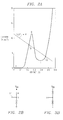
- the series connection of two RTDs and their bistable operating points 16 and 18 is illustrated in FIG.3. It is this configuration which is exploited by this invention.
- a dynamic shift register stores the binary ones and zeroes in capacitors, normally the parasitic capacitances of the circuit interconnects.
- the data stream is asynchronous, i.e. stops and starts.
- the data may be lost due to capacitor leakage if the clock is stopped for too long a period. The faster the clock the smaller the capacitor and the sooner the data is lost if the clock stops.
- a static shift register can be used to overcome this difficulty.
- static circuits require more components and hence device and interconnect delays. Many times these circuits also dissipate considerably more power than their dynamic counterparts. As seen in FIG.3 both stable points 16 and 18 are at low current.
- the present invention includes a cascaded pair of RTDs to achieve a bistable operating state.
- a means of setting the binary state of this bistable pair is also provided.
- a method of providing isolation and gain using a buffer amplifier between the two pairs of RTDs is also provided.
- this ultra high speed static shift register invention After the receipt of data transmitted at a rate above a gigahertz, it is often desired to store this data and then transmit the same data at a slower rate so that the data may be stored and processed by slower more conventional digital systems.
- This slower clock frequency may be preceded by a short delay in order to be synchronous with the downstream clock frequency if desired.
- the data in the shift register may then be clocked out at a lower rate.
- a source follower is provided to drive downstream digital processing circuitry where capacitive loading may otherwise cause problems.
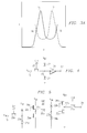
- a generic shift register stage there is shown a series connection of RTDs 22 and 24 whose I-V characteristics are matched and which are supplied with power from V dd to ground. This is the bistable configuration previously described in reference to FIG. 3 which showed peak currents at 15 and 17.
- a low voltage state at connection 23 will be considered a binary O and a high voltage state at connection 23 as a binary 1.
- clock 21 is applied to switching transistor 20, the voltage 19 is tied directly to the junction 23 of the series connected RTDs 22 and 24. If the voltage 19 is lower than peak 15, 23 is forced to the stable point 16, the binary 0 state. Conversely, when the voltage 19 is higher than peak 17, 23 is forced to the stable point 18, the binary 1 state.
- the clock 21 now turns “OFF" switching transistor 21 and the forced state at 23 remains.
- To facilitate the driving of the next stage of the shift register buffer amplifier 26 is connected between 23 and the output node 27.
- This buffer amplifier provides isolation between 23 and the next stage as well as providing gain to insure that the next stage receives adequate power to set that stage at a binary 1 or 0.
- FIG.5 A more complete circuit of a segment of an ultra high speed shift register is shown in FIG.5 in which the buffer amplifier consists of an enhancement FET 30 to supply gain and a depletion load device 28.
- the buffer amplifier consists of an enhancement FET 30 to supply gain and a depletion load device 28.
- suffix letters "a" and "b” have been added to distinguish the first stage of the shift register from the second stage to simplify description.
- the unput voltage at 19 is at binary 1, high voltage.
- Clock 21 turns “ON” switch transistor 20a.
- the corresponding switch transistor 20b in the second stage of the shift register is driven by 32 which is the complement of 21 which turns "OFF" transistor 20b, As discussed previously, 19 sets connection 23a to the binary 1 state. Connection 23a is common with the gate of 30a.
- RTD 35a replaces the depletion load transistor 28a of FIG.5.
- I-V characteristics of RTD's may be tailored to the application.
- RTD 35a must supply enough voltage when amplifier 30a is in the low current state to force 23b to the binary 1 state when switch 20b is closed.
- 30a will be in the high current state and force 23b to the binary 0 state.
- the design goals for 35a and 35b are (1) low bias current and (2) adequate logic swing with good noise margin. From the device point of view this means that the peak voltage of 35a and 35b should be approximately half of the swing of 23a and 23b respectively.
- the step-by-step binary sequence and polarities are the same as FIG 5.
- FIG.7 shows another preferred embodiment of this invention.
- the buffer stage between the static latching pairs of RTDs is a noninverting source follower consisting of enhancement mode FET 30 and a source depletion load device 28.
- the complementary clocking is the same as the previous circuits but in this case there is no inversion between the two shift register stages. In this case when 23 a is forced to a binary state by clock phase 21, 23b is forced to the same binary state during the complementary phase 32. All the other components function as previously described.
Landscapes
- Engineering & Computer Science (AREA)
- Physics & Mathematics (AREA)
- Chemical & Material Sciences (AREA)
- Nanotechnology (AREA)
- Mathematical Physics (AREA)
- Theoretical Computer Science (AREA)
- Crystallography & Structural Chemistry (AREA)
- Nonlinear Science (AREA)
- Logic Circuits (AREA)
- Shift Register Type Memory (AREA)
- Radar Systems Or Details Thereof (AREA)
Applications Claiming Priority (2)
| Application Number | Priority Date | Filing Date | Title |
|---|---|---|---|
| US2456896P | 1996-08-26 | 1996-08-26 | |
| US24568P | 1996-08-26 |
Publications (3)
| Publication Number | Publication Date |
|---|---|
| EP0827156A2 true EP0827156A2 (fr) | 1998-03-04 |
| EP0827156A3 EP0827156A3 (fr) | 1999-04-07 |
| EP0827156B1 EP0827156B1 (fr) | 2003-02-26 |
Family
ID=21821261
Family Applications (1)
| Application Number | Title | Priority Date | Filing Date |
|---|---|---|---|
| EP97306413A Expired - Lifetime EP0827156B1 (fr) | 1996-08-26 | 1997-08-22 | Registre à décalage utilisant des éléments à résistance négative |
Country Status (5)
| Country | Link |
|---|---|
| EP (1) | EP0827156B1 (fr) |
| JP (1) | JPH1092188A (fr) |
| KR (1) | KR19980019001A (fr) |
| DE (1) | DE69719264T2 (fr) |
| TW (1) | TW359030B (fr) |
Cited By (7)
| Publication number | Priority date | Publication date | Assignee | Title |
|---|---|---|---|---|
| US8819376B2 (en) | 2012-04-23 | 2014-08-26 | Hewlett-Packard Development Company, L. P. | Merging arrays using shiftable memory |
| US8854860B2 (en) | 2011-10-28 | 2014-10-07 | Hewlett-Packard Development Company, L.P. | Metal-insulator transition latch |
| US9331700B2 (en) | 2011-10-28 | 2016-05-03 | Hewlett Packard Enterprise Development Lp | Metal-insulator phase transition flip-flop |
| US9384824B2 (en) | 2012-07-10 | 2016-07-05 | Hewlett Packard Enterprise Development Lp | List sort static random access memory |
| US9431074B2 (en) | 2012-03-02 | 2016-08-30 | Hewlett Packard Enterprise Development Lp | Shiftable memory supporting bimodal storage |
| US9606746B2 (en) | 2011-10-27 | 2017-03-28 | Hewlett Packard Enterprise Development Lp | Shiftable memory supporting in-memory data structures |
| US9846565B2 (en) | 2011-10-27 | 2017-12-19 | Hewlett Packard Enterprise Development Lp | Shiftable memory employing ring registers |
Families Citing this family (6)
| Publication number | Priority date | Publication date | Assignee | Title |
|---|---|---|---|---|
| US6456214B1 (en) * | 2000-09-27 | 2002-09-24 | Raytheon Company | High-speed comparator utilizing resonant tunneling diodes and associated method |
| KR100588612B1 (ko) * | 2004-12-22 | 2006-06-14 | 한국과학기술원 | Current Mode Logic(CML) 입력드라이빙 회로구성과 MonostableBistable Transition logicelement(MOBILE)를 이용한 터넬링 다이오드로직 회로 |
| EP2727114B1 (fr) | 2011-06-28 | 2020-04-22 | Hewlett-Packard Enterprise Development LP | Mémoire décalable |
| EP2771885B1 (fr) | 2011-10-27 | 2021-12-01 | Valtrus Innovations Limited | Mémoire décalable prenant en charge une opération atomique |
| KR101660611B1 (ko) | 2012-01-30 | 2016-09-27 | 휴렛 팩커드 엔터프라이즈 디벨롭먼트 엘피 | 워드 시프트 정적 랜덤 액세스 메모리(ws-sram) |
| WO2013130109A1 (fr) | 2012-03-02 | 2013-09-06 | Hewlett-Packard Development Company L.P. | Défragmentation de mémoire pouvant être décalée |
Family Cites Families (5)
| Publication number | Priority date | Publication date | Assignee | Title |
|---|---|---|---|---|
| BE623371A (fr) * | 1961-10-10 | |||
| JPS63261600A (ja) * | 1987-04-17 | 1988-10-28 | Fujitsu Ltd | シフトレジスタ回路 |
| US4902912A (en) * | 1987-07-01 | 1990-02-20 | American Telephone And Telegraph Company, At&T Bell Laboratories | Apparatus including resonant-tunneling device having multiple-peak current-voltage characteristics |
| JPS6451718A (en) * | 1987-08-21 | 1989-02-28 | Nec Corp | Counter circuit |
| US5444751A (en) * | 1993-09-24 | 1995-08-22 | Massachusetts Institute Of Technology | Tunnel diode shift register utilizing tunnel diode coupling |
-
1997
- 1997-08-22 EP EP97306413A patent/EP0827156B1/fr not_active Expired - Lifetime
- 1997-08-22 DE DE69719264T patent/DE69719264T2/de not_active Expired - Lifetime
- 1997-08-26 JP JP9229971A patent/JPH1092188A/ja active Pending
- 1997-08-26 KR KR1019970040870A patent/KR19980019001A/ko not_active Ceased
- 1997-10-06 TW TW086112295A patent/TW359030B/zh not_active IP Right Cessation
Cited By (7)
| Publication number | Priority date | Publication date | Assignee | Title |
|---|---|---|---|---|
| US9606746B2 (en) | 2011-10-27 | 2017-03-28 | Hewlett Packard Enterprise Development Lp | Shiftable memory supporting in-memory data structures |
| US9846565B2 (en) | 2011-10-27 | 2017-12-19 | Hewlett Packard Enterprise Development Lp | Shiftable memory employing ring registers |
| US8854860B2 (en) | 2011-10-28 | 2014-10-07 | Hewlett-Packard Development Company, L.P. | Metal-insulator transition latch |
| US9331700B2 (en) | 2011-10-28 | 2016-05-03 | Hewlett Packard Enterprise Development Lp | Metal-insulator phase transition flip-flop |
| US9431074B2 (en) | 2012-03-02 | 2016-08-30 | Hewlett Packard Enterprise Development Lp | Shiftable memory supporting bimodal storage |
| US8819376B2 (en) | 2012-04-23 | 2014-08-26 | Hewlett-Packard Development Company, L. P. | Merging arrays using shiftable memory |
| US9384824B2 (en) | 2012-07-10 | 2016-07-05 | Hewlett Packard Enterprise Development Lp | List sort static random access memory |
Also Published As
| Publication number | Publication date |
|---|---|
| DE69719264T2 (de) | 2003-11-06 |
| JPH1092188A (ja) | 1998-04-10 |
| EP0827156A3 (fr) | 1999-04-07 |
| EP0827156B1 (fr) | 2003-02-26 |
| KR19980019001A (ko) | 1998-06-05 |
| TW359030B (en) | 1999-05-21 |
| DE69719264D1 (de) | 2003-04-03 |
Similar Documents
| Publication | Publication Date | Title |
|---|---|---|
| US5930323A (en) | Ultra fast shift register using resonant tunnel diodes | |
| EP0809888B1 (fr) | Nouvelle famille logique utilisant des comutateurs a deux bornes en chalcogenure en tant que portes logiques | |
| Inokawa et al. | A multiple-valued logic and memory with combined single-electron and metal-oxide-semiconductor transistors | |
| US5024993A (en) | Superconducting-semiconducting circuits, devices and systems | |
| EP0827156B1 (fr) | Registre à décalage utilisant des éléments à résistance négative | |
| US3986043A (en) | CMOS digital circuits with active shunt feedback amplifier | |
| US5815008A (en) | Resonant tunneling diode structures for funtionally complete low-power logic | |
| US5903170A (en) | Digital logic design using negative differential resistance diodes and field-effect transistors | |
| JP2001148628A (ja) | 量子力学的トンネル構造を使用するcmosダイナミック・ロジック回路 | |
| US6566914B2 (en) | Sense amplifier having reduced Vt mismatch in input matched differential pair | |
| US7154918B2 (en) | Multiplexer circuit for converting parallel data into serial data at high speed and synchronized with a clock signal | |
| US4623801A (en) | Divide-by-two frequency divider | |
| US5424656A (en) | Continuous superconductor to semiconductor converter circuit | |
| US6362660B1 (en) | CMOS latch and register circuitry using quantum mechanical tunneling structures | |
| US6180984B1 (en) | Integrated circuit impedance device and method of manufacture therefor | |
| JPS61262314A (ja) | Cmos技術による静的双安定フリツプフロツプ回路 | |
| US5030853A (en) | High speed logic and memory family using ring segment buffer | |
| Hida et al. | 0.6 V suppy voltage 0.25/spl mu/m E/D-HJFET (IS/sup 3/T) LSI technology for low power consumption and high speed LSIs | |
| Ghoshal et al. | Josephson-CMOS memories | |
| Allison et al. | Silicon-on-sapphire complementary MOS memory cells | |
| US5134319A (en) | Bicmos differential amplifier having improved switching speed | |
| Moore et al. | Metal-oxide-semiconductor field-effect devices for micropower logic circuitry | |
| JP2931586B1 (ja) | 広い電圧許容範囲を有する入出力回路 | |
| Glösekötter et al. | Circuit and application aspects of tunnelling devices in a MOBILE configuration | |
| US5105105A (en) | High speed logic and memory family using ring segment buffer |
Legal Events
| Date | Code | Title | Description |
|---|---|---|---|
| PUAI | Public reference made under article 153(3) epc to a published international application that has entered the european phase |
Free format text: ORIGINAL CODE: 0009012 |
|
| AK | Designated contracting states |
Kind code of ref document: A2 Designated state(s): DE FR GB IT NL |
|
| PUAL | Search report despatched |
Free format text: ORIGINAL CODE: 0009013 |
|
| AK | Designated contracting states |
Kind code of ref document: A3 Designated state(s): AT BE CH DE DK ES FI FR GB GR IE IT LI LU MC NL PT SE |
|
| 17P | Request for examination filed |
Effective date: 19991005 |
|
| AKX | Designation fees paid |
Free format text: DE FR GB IT NL |
|
| 17Q | First examination report despatched |
Effective date: 20000620 |
|
| GRAG | Despatch of communication of intention to grant |
Free format text: ORIGINAL CODE: EPIDOS AGRA |
|
| GRAG | Despatch of communication of intention to grant |
Free format text: ORIGINAL CODE: EPIDOS AGRA |
|
| GRAH | Despatch of communication of intention to grant a patent |
Free format text: ORIGINAL CODE: EPIDOS IGRA |
|
| GRAH | Despatch of communication of intention to grant a patent |
Free format text: ORIGINAL CODE: EPIDOS IGRA |
|
| GRAH | Despatch of communication of intention to grant a patent |
Free format text: ORIGINAL CODE: EPIDOS IGRA |
|
| GRAA | (expected) grant |
Free format text: ORIGINAL CODE: 0009210 |
|
| AK | Designated contracting states |
Designated state(s): DE FR GB IT NL |
|
| PG25 | Lapsed in a contracting state [announced via postgrant information from national office to epo] |
Ref country code: NL Free format text: LAPSE BECAUSE OF FAILURE TO SUBMIT A TRANSLATION OF THE DESCRIPTION OR TO PAY THE FEE WITHIN THE PRESCRIBED TIME-LIMIT Effective date: 20030226 Ref country code: IT Free format text: LAPSE BECAUSE OF FAILURE TO SUBMIT A TRANSLATION OF THE DESCRIPTION OR TO PAY THE FEE WITHIN THE PRE;WARNING: LAPSES OF ITALIAN PATENTS WITH EFFECTIVE DATE BEFORE 2007 MAY HAVE OCCURRED AT ANY TIME BEFORE 2007. THE CORRECT EFFECTIVE DATE MAY BE DIFFERENT FROM THE ONE RECORDED.SCRIBED TIME-LIMIT Effective date: 20030226 |
|
| REG | Reference to a national code |
Ref country code: GB Ref legal event code: FG4D |
|
| REF | Corresponds to: |
Ref document number: 69719264 Country of ref document: DE Date of ref document: 20030403 Kind code of ref document: P |
|
| NLV1 | Nl: lapsed or annulled due to failure to fulfill the requirements of art. 29p and 29m of the patents act | ||
| ET | Fr: translation filed | ||
| PLBE | No opposition filed within time limit |
Free format text: ORIGINAL CODE: 0009261 |
|
| STAA | Information on the status of an ep patent application or granted ep patent |
Free format text: STATUS: NO OPPOSITION FILED WITHIN TIME LIMIT |
|
| 26N | No opposition filed |
Effective date: 20031127 |
|
| PGFP | Annual fee paid to national office [announced via postgrant information from national office to epo] |
Ref country code: GB Payment date: 20120726 Year of fee payment: 16 |
|
| PGFP | Annual fee paid to national office [announced via postgrant information from national office to epo] |
Ref country code: DE Payment date: 20120831 Year of fee payment: 16 Ref country code: FR Payment date: 20120809 Year of fee payment: 16 |
|
| GBPC | Gb: european patent ceased through non-payment of renewal fee |
Effective date: 20130822 |
|
| PG25 | Lapsed in a contracting state [announced via postgrant information from national office to epo] |
Ref country code: DE Free format text: LAPSE BECAUSE OF NON-PAYMENT OF DUE FEES Effective date: 20140301 |
|
| REG | Reference to a national code |
Ref country code: FR Ref legal event code: ST Effective date: 20140430 |
|
| REG | Reference to a national code |
Ref country code: DE Ref legal event code: R119 Ref document number: 69719264 Country of ref document: DE Effective date: 20140301 |
|
| PG25 | Lapsed in a contracting state [announced via postgrant information from national office to epo] |
Ref country code: GB Free format text: LAPSE BECAUSE OF NON-PAYMENT OF DUE FEES Effective date: 20130822 |
|
| PG25 | Lapsed in a contracting state [announced via postgrant information from national office to epo] |
Ref country code: FR Free format text: LAPSE BECAUSE OF NON-PAYMENT OF DUE FEES Effective date: 20130902 |