EP0827220A2 - Méthodes et compositions pour optimiser les caractéristiques interfaciales de transducteurs utilisés dans des dispositifs de stockage de données - Google Patents
Méthodes et compositions pour optimiser les caractéristiques interfaciales de transducteurs utilisés dans des dispositifs de stockage de données Download PDFInfo
- Publication number
- EP0827220A2 EP0827220A2 EP97114191A EP97114191A EP0827220A2 EP 0827220 A2 EP0827220 A2 EP 0827220A2 EP 97114191 A EP97114191 A EP 97114191A EP 97114191 A EP97114191 A EP 97114191A EP 0827220 A2 EP0827220 A2 EP 0827220A2
- Authority
- EP
- European Patent Office
- Prior art keywords
- spacer
- selecting
- electronegativity
- data storage
- storage device
- Prior art date
- Legal status (The legal status is an assumption and is not a legal conclusion. Google has not performed a legal analysis and makes no representation as to the accuracy of the status listed.)
- Withdrawn
Links
Images


Classifications
-
- G—PHYSICS
- G01—MEASURING; TESTING
- G01R—MEASURING ELECTRIC VARIABLES; MEASURING MAGNETIC VARIABLES
- G01R33/00—Arrangements or instruments for measuring magnetic variables
- G01R33/02—Measuring direction or magnitude of magnetic fields or magnetic flux
- G01R33/06—Measuring direction or magnitude of magnetic fields or magnetic flux using galvano-magnetic devices
- G01R33/09—Magnetoresistive devices
- G01R33/093—Magnetoresistive devices using multilayer structures, e.g. giant magnetoresistance sensors
-
- B—PERFORMING OPERATIONS; TRANSPORTING
- B82—NANOTECHNOLOGY
- B82Y—SPECIFIC USES OR APPLICATIONS OF NANOSTRUCTURES; MEASUREMENT OR ANALYSIS OF NANOSTRUCTURES; MANUFACTURE OR TREATMENT OF NANOSTRUCTURES
- B82Y10/00—Nanotechnology for information processing, storage or transmission, e.g. quantum computing or single electron logic
-
- B—PERFORMING OPERATIONS; TRANSPORTING
- B82—NANOTECHNOLOGY
- B82Y—SPECIFIC USES OR APPLICATIONS OF NANOSTRUCTURES; MEASUREMENT OR ANALYSIS OF NANOSTRUCTURES; MANUFACTURE OR TREATMENT OF NANOSTRUCTURES
- B82Y25/00—Nanomagnetism, e.g. magnetoimpedance, anisotropic magnetoresistance, giant magnetoresistance or tunneling magnetoresistance
-
- B—PERFORMING OPERATIONS; TRANSPORTING
- B82—NANOTECHNOLOGY
- B82Y—SPECIFIC USES OR APPLICATIONS OF NANOSTRUCTURES; MEASUREMENT OR ANALYSIS OF NANOSTRUCTURES; MANUFACTURE OR TREATMENT OF NANOSTRUCTURES
- B82Y40/00—Manufacture or treatment of nanostructures
-
- G—PHYSICS
- G11—INFORMATION STORAGE
- G11B—INFORMATION STORAGE BASED ON RELATIVE MOVEMENT BETWEEN RECORD CARRIER AND TRANSDUCER
- G11B5/00—Recording by magnetisation or demagnetisation of a record carrier; Reproducing by magnetic means; Record carriers therefor
- G11B5/127—Structure or manufacture of heads, e.g. inductive
- G11B5/33—Structure or manufacture of flux-sensitive heads, i.e. for reproduction only; Combination of such heads with means for recording or erasing only
- G11B5/39—Structure or manufacture of flux-sensitive heads, i.e. for reproduction only; Combination of such heads with means for recording or erasing only using magneto-resistive devices or effects
- G11B5/3903—Structure or manufacture of flux-sensitive heads, i.e. for reproduction only; Combination of such heads with means for recording or erasing only using magneto-resistive devices or effects using magnetic thin film layers or their effects, the films being part of integrated structures
-
- H—ELECTRICITY
- H01—ELECTRIC ELEMENTS
- H01F—MAGNETS; INDUCTANCES; TRANSFORMERS; SELECTION OF MATERIALS FOR THEIR MAGNETIC PROPERTIES
- H01F41/00—Apparatus or processes specially adapted for manufacturing or assembling magnets, inductances or transformers; Apparatus or processes specially adapted for manufacturing materials characterised by their magnetic properties
- H01F41/14—Apparatus or processes specially adapted for manufacturing or assembling magnets, inductances or transformers; Apparatus or processes specially adapted for manufacturing materials characterised by their magnetic properties for applying magnetic films to substrates
- H01F41/30—Apparatus or processes specially adapted for manufacturing or assembling magnets, inductances or transformers; Apparatus or processes specially adapted for manufacturing materials characterised by their magnetic properties for applying magnetic films to substrates for applying nanostructures, e.g. by molecular beam epitaxy [MBE]
- H01F41/302—Apparatus or processes specially adapted for manufacturing or assembling magnets, inductances or transformers; Apparatus or processes specially adapted for manufacturing materials characterised by their magnetic properties for applying magnetic films to substrates for applying nanostructures, e.g. by molecular beam epitaxy [MBE] for applying spin-exchange-coupled multilayers, e.g. nanostructured superlattices
-
- H—ELECTRICITY
- H10—SEMICONDUCTOR DEVICES; ELECTRIC SOLID-STATE DEVICES NOT OTHERWISE PROVIDED FOR
- H10N—ELECTRIC SOLID-STATE DEVICES NOT OTHERWISE PROVIDED FOR
- H10N50/00—Galvanomagnetic devices
- H10N50/10—Magnetoresistive devices
-
- H—ELECTRICITY
- H10—SEMICONDUCTOR DEVICES; ELECTRIC SOLID-STATE DEVICES NOT OTHERWISE PROVIDED FOR
- H10N—ELECTRIC SOLID-STATE DEVICES NOT OTHERWISE PROVIDED FOR
- H10N50/00—Galvanomagnetic devices
- H10N50/80—Constructional details
- H10N50/85—Materials of the active region
-
- G—PHYSICS
- G11—INFORMATION STORAGE
- G11B—INFORMATION STORAGE BASED ON RELATIVE MOVEMENT BETWEEN RECORD CARRIER AND TRANSDUCER
- G11B5/00—Recording by magnetisation or demagnetisation of a record carrier; Reproducing by magnetic means; Record carriers therefor
- G11B5/127—Structure or manufacture of heads, e.g. inductive
- G11B5/33—Structure or manufacture of flux-sensitive heads, i.e. for reproduction only; Combination of such heads with means for recording or erasing only
- G11B5/39—Structure or manufacture of flux-sensitive heads, i.e. for reproduction only; Combination of such heads with means for recording or erasing only using magneto-resistive devices or effects
- G11B2005/3996—Structure or manufacture of flux-sensitive heads, i.e. for reproduction only; Combination of such heads with means for recording or erasing only using magneto-resistive devices or effects large or giant magnetoresistive effects [GMR], e.g. as generated in spin-valve [SV] devices
-
- G—PHYSICS
- G11—INFORMATION STORAGE
- G11B—INFORMATION STORAGE BASED ON RELATIVE MOVEMENT BETWEEN RECORD CARRIER AND TRANSDUCER
- G11B5/00—Recording by magnetisation or demagnetisation of a record carrier; Reproducing by magnetic means; Record carriers therefor
- G11B5/40—Protective measures on heads, e.g. against excessive temperature
Definitions
- This invention relates to methods and compositions for optimizing the interfacial properties of data storage devices, such as spin valve sensors and giant magnetoresitance (GMR) sensors.
- data storage devices such as spin valve sensors and giant magnetoresitance (GMR) sensors.
- GMR giant magnetoresitance
- Still another object of the present invention is to maximize the signal output, as represented by % ⁇ R/R of spin valve sensors and giant magnetoresistance (GMR) sensors.
- Yet another object of this invention is to maximize the corrosion resistance of spin valve sensors and giant magnetoresistance sensors.
- the present invention proposes an empirical relationship between % ⁇ R/R and the electronegativity difference between adjacent FM layers and conductive spacers in spin valve and GMR sensors.
- Such a general empirical relationship applies to both spin valve and GMR sensors, and shows that % ⁇ R/R response is a function of the electronegativity mismatch between adjacent FM layers and conductive spacers.
- ⁇ mismatch in electronegativities
- Each chemical element has a work function ⁇ from which the ⁇ of that element is computed by either equations (1a) or (1b) that are equivalent.
- the ⁇ of such alloys has been found to be an additive property of the constituents of the alloy, so that the ⁇ of the alloy is the sum of the products of the atomic fraction of any element in the alloy times the electronegativity of that element summed over all elements constituting the alloy, as expressed in equation (2).
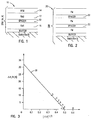
- Fig. 2 illustrates the use of the present inventive concept in a giant magnetoresistive (GMR) sensor 20.
- the GMR sensor 20 is a sandwich structure formed of a plurality of layers, such as FM, that are separated by a plurality of conductive spacers 22.
- the FM/spacer structure can have a multiplicity of 5 to 75 repeat units of FM/spacers.
- the electronegativities of each of the successive layers FM are substantially matched or their difference in ⁇ is minimized with the electronegativity of the contiguous spacers 22.
- Prior art methods for fabricating spin valve and GMR sensors included combining spacers made of an adequately electrically conductive material such as Au, Ag or Cu, with layers of FM materials such as FeCo alloy or NiFe alloy, or elements Fe, Co and Ni, without regard to the electronegativity matching between the successive FM layers and conductive spacers. These prior art methods are mainly based on trial and error studies.
- This example illustrates that the atomic fraction of the electronegativities ( ⁇ 's) of the elements of any alloy conductor or ferromagnet formed of any number of elements, i.e., ternary, quaternary, etc., can be used to calculate the electronegativity of the alloy.
- Table I it is possible to closely match the electronegativities of the conductors and the ferromagnets. For example, having selected Cu 3 Pt as the conductor of choice, it would be desirable to select a FM material having a close electronegativity. Table I indicates that one of the closest materials whose electronegativity matches that of Cu 3 Pt is NiMn, since the average electronegativity of Ni 3 Mn is 2.02 and ⁇ ⁇ 0
- a superlattice intermetallic compound having an electronegativity of 2.02 may be matched with Cu 3 Pt.
- the matching of two superlattice structures is desirable in that these ordered structures will improve the thermal stability of the device containing them, since additional external thermal energy would be required to disorder one or both superlattice structures before the elements contained in superlattice were free to diffuse at the interface. This additional energy ranges between 0.1 eV to 0.3 eV above the activation energy for cross diffusion at the interface between the conductor spacer and the FM layer.
- Point D on curve S1 represents the following composition:Co - Cu - CO, where the first element (Co) is the unpinned FM layer FM1, the second element [Cu] is the conductive spacer 12, and the third element [Co] is the pinned FM layer FM2.
- the composition of this example yields a % ⁇ R/R of approximately 9.5%.
- Point H on curve S1 represents Ni- Cu -Ni, where the first element (Ni) is the unpinned FM layer FM1, the second element [Cu] is the conductive spacer 12, and the third element [Ni] is the pinned FM layer FM2.
- the composition of this example yields a % ⁇ R/R of approximately 2.5%.
- Point I on curve S1 represents [80Ni 20Fe]-[Pt]-[80Ni 20Fe], where the first element [80Ni 20Fe] is the unpinned FM layer FM1, the second element [Pt] is the conductive spacer 12, and the third element [80Ni 20Fe] is the pinned FM layer FM2.
- the composition of this example yields a % ⁇ R/R of approximately 0.3%.
- Point K on curve S1 represents [80Ni 20Fe]-[Al]-[80Ni 20Fe], where the first element [80Ni 20Fe] is the unpinned FM layer FM1, the second element [Al] is the conductive spacer 12, and the third element [80Ni 20 Fe] is the pinned FM layer FM2.
- 1/2 between Al and its adjacent NiFe layer FM1 is approximately 0.6/eV, which is greater than the intercept point value of 0.5 eV. In this and other similar examples where
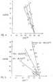
- Fig. 4 graphically illustrates the linear relationships between the % ⁇ R/R of the spin valve sensor 10 (Fig. 1) relative to the square root of the absolute value of the electronegativity difference (
- the response is shown at three different measurement temperatures, that is, 300°K, 200°K and 100°K.
- the conductive spacer separating the FMs is generally between 18A° and 30° thick, while the FMs generally range between 30A° and 120A° with an optimum thickness typically at 60A° each.
- Fig. 5 graphically illustrates linear relationships between % ⁇ R/R of the GMR sensor 20 (Fig. 2) relative to the square root of the electronegativity difference
- the curves G1, G2, G3 may be expressed generally by the following equations (6), (7) and (8), that continue to confirm equations (3) and (4).
- the present analysis recognizes the need for optimizing the roughness of the interface for maximizing % ⁇ R/R for any particular interface. Accordingly, the curves G1, G2, G3 take into consideration the fact that different experimenters may conduct their experiments under different conditions, such as different substrate temperatures, different deposition rates, different Argon background sputtering pressure, and thus will realize different degrees of interfacial roughness. Again we reiterate that the interfacial surface roughness will vary the slopes of curves G1, G2 and G3 and that some optimum roughness exists that maximizes % ⁇ R/R for any interface ⁇ of the FM and spacer layers.
- points R1 and S1 correspond to the respective compositions of points J1, H1, and M1 along the first peak curve G1.
- V1 is Ni30-Co70
- W1 is Ni50-Co50
- X1 is Ni70-Co30
- Y1 is Ni.
- Fig. 6 graphically illustrates three linear relationships between % ⁇ R/R of the GMR sensor 20 (Fig. 2) relative to the square root of the electronegativity difference
- Curve R1 may be expressed by the following equation (9), and relates to the GMR first peak: % ⁇ R/R ⁇ 330 - 660
- Curve R2 may be expressed by the following equation (10), and relates to the second GMR peak: (10) % ⁇ R/R ⁇ 158 - 316 (
- the exemplary compositions are expressed as follows X-Y, where element X represents the material for the FM layers FM, and element "Y" represents the material for the conductive spacers 22.
- points m1 and n1 correspond to the respective compositions of points i1 (Co/Cu), and j1 (Co/Ag) along the first peak curve G1.
- Point "p” relates to the GMR structure Fe - Cu.
- This structure presents an almost perfect electronegativity match i. e., ( ⁇ ⁇ 0) between the Fe and Cu layers, nonetheless, this structure does not provide a high % ⁇ R/R since Fe is a BCC element, while Cu is a FCC element. Accordingly extremely inferior % ⁇ R/R is obtained and equations (3 and 4) are not obeyed due to potential barriers created by the lattice type mismatch, that is, BCC/FCC.
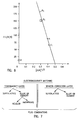
- Fig. 9 shows two graphs SL3, SL4, plotting the electrical resistivity in micro ohmcm versus the atomic composition for the Cu-Pt superlattice system.
- Graph SL3 illustrates the relationship for alloys that are quenched and cold worked (disordered state).
- Graph SL4 illustrates the relationship for alloys that are annealed at 300°C for rendering an ordered superlattice structure.
- Fig. 9 further shows that the specific electrical resistivities of the ordered superlattice may be reduced significantly by annealing the alloys at two critical points CP3 (25% atomic percent Pt), and CP4 (50% atomic percent Pt).
- the two alloy series in examples 24 and 25 may be annealed at between 120 °C to 250 °C in thin film form for approximately 0.5 hour to 4 hours to form the superlattice at appropriate composition.
- the present invention proposes the use of superlattices processed at or near critical points CP or within any of the shaded regions in the CuAu binary systemor the CuPtbinary system.
- the shaded regions define the composition range within which some degree of superlattice order will occur and which may be used advantageously.
- the most advantageous compositions from a resistivity point of view are a 25 and 50 atomic % for both the CuAu and CuPt.
- a superlattice spacer 22 will provide a large mean free path in the spacer while simultaneously minimizing the electronegativity difference
- 50:50 CuAu superlattice alloy (Fig. 9) exhibits a resistivity of about 3.5 ⁇ -cm, which is similar to the resistivity of gold, and an average electronegativity ( ⁇ ) of approximately 2.07 eV.
- a 50:50 CuAu superlattice ( Figure 5) is used as a spacer, while an Ni 3 Fe superlattice composition forms the FM layers.
- the average electronegativity of the 50:50 CuAu superlattice is about 2.07, which has an absolute electronegativeity difference of about 0.01 with N 13 Fe.
- one method for processing the superlattice is to anneal the alloys between 120°C to 250°C for 10 to 200 minutes.
- An alternative method is to deposit the superlattice alloys by sputtering or evaporation, at a relatively low rate, on a sufficiently heated substrate. This slow deposition process could form the superlattice structure without the need for annealing.
- the alloys that are used to achieve the preceding objectives are from the group constituting Fe, Ni, Co or any combination of these elements, and alloys thereof which, may be alloyeed with elements or combination thereof from the group consisting of Au, Cu, Mn, Ti, V, Pt, Pd, Ru, Ir, Sn, Ta, Nb, Rh, N, C, Zr, Hf, Y, La, and rare earth elements, either in crystalline FCC or BCC form or in amorphous form containing a combination of the above elements.
- a group of quaternary FM alloys with minimal magnetostriction includes: [48Co - 29Ni - 23Fe] 1-yPd. [26Co - 44Ni - 30Fe] 1-yPd.
- y represents the atomic fraction
- these alloys display near zero magnetostriction and low overcivity. More specifically, the following alloys have near zero magnetostriction and have ⁇ values of 2.13.
- Each alloy can be matched with the superlattice composite conductive spacer of CuPt whose ⁇ is approximately 2.12. 33.6Co - 20.3Ni - 16.1Fe - 30Pd. 18.2Co - 30.8Ni - 21Fe - 30Pd.
- Fig. 10 illustrates the use of single crystals in the spin valve sensor 10 of Fig. 1.
- the surface crystalline orientation of the substrate has been selected to be 111.
- the subsequent single crystal layers that are formed on top of the substrate will automatically assume the same 111 surface orientation. It is an object of the present invention to match the electronegativities of the selected crystalline orientation or face, which in this example is 111, of the juxtaposed layers, rather than to match the average electronegativities of these layers.
- Fig. 11 illustrates the use of polycrystals in the spin valve sensor 10 of Fig. 1.
- the crystalline orientation of the substrate is random, and therefore the three main crystallographic orientations, i.e., 100, 110, 111 have approximately the same frequency of surface occupancy on the substrate.
- the subsequent polycrystal layers FM and AFM that are formed on top of the substrate will automatically assume the same random orientation as the substrate by epitaxy of the underlying polycrystals of the prior spacer or FM layer FM. It is an object of the present invention to match the average electronegativity of each layer to the average electronegativity of the adjacent layers.
- the spin valve sensor 10 is formed by selecting the desired spacer material. Subsequently, the FM layers FM1 and FM2 are selected such that their average electronegativities match or substantially approximate the average electronegativity of the selected spacer 12.
- the following example 29 illustrates the impact of the mismatch of the electronegativity (
- the selection of crystal orientation, 111, 100 or 110 can be accomplished by selecting a single crystal substrate such as single crystal magnesium oxide with surface orientations of either 111, 100 or 110.
- a single orientation for example 111 of the substrate and subsequently selecting a ferromagnet and conductive spacer whose ⁇ 's are minimized, and subsequently depositing alternating layers of FM and conductive spacers on such an oriented substrate, results in % ⁇ R/R's that will be greater than randomly oriented polycrystalline structures.
- AgAu alloys may be used as well with Au less than 25 atomic %.
Landscapes
- Engineering & Computer Science (AREA)
- Nanotechnology (AREA)
- Chemical & Material Sciences (AREA)
- Physics & Mathematics (AREA)
- Crystallography & Structural Chemistry (AREA)
- Manufacturing & Machinery (AREA)
- Power Engineering (AREA)
- Condensed Matter Physics & Semiconductors (AREA)
- General Physics & Mathematics (AREA)
- Theoretical Computer Science (AREA)
- Mathematical Physics (AREA)
- Spectroscopy & Molecular Physics (AREA)
- Hall/Mr Elements (AREA)
- Micromachines (AREA)
- Magnetic Heads (AREA)
Applications Claiming Priority (2)
| Application Number | Priority Date | Filing Date | Title |
|---|---|---|---|
| US08/702,977 US5793279A (en) | 1996-08-26 | 1996-08-26 | Methods and compositions for optimizing interfacial properties of magnetoresistive sensors |
| US702977 | 1996-08-26 |
Publications (2)
| Publication Number | Publication Date |
|---|---|
| EP0827220A2 true EP0827220A2 (fr) | 1998-03-04 |
| EP0827220A3 EP0827220A3 (fr) | 1999-06-09 |
Family
ID=24823431
Family Applications (2)
| Application Number | Title | Priority Date | Filing Date |
|---|---|---|---|
| EP97114191A Withdrawn EP0827220A3 (fr) | 1996-08-26 | 1997-08-18 | Méthodes et compositions pour optimiser les caractéristiques interfaciales de transducteurs utilisés dans des dispositifs de stockage de données |
| EP97114774A Withdrawn EP0827221A3 (fr) | 1996-08-26 | 1997-08-26 | Méthodes et compositions pour optimiser les caractéristiques interfaciales de capteurs magnétorésistifs |
Family Applications After (1)
| Application Number | Title | Priority Date | Filing Date |
|---|---|---|---|
| EP97114774A Withdrawn EP0827221A3 (fr) | 1996-08-26 | 1997-08-26 | Méthodes et compositions pour optimiser les caractéristiques interfaciales de capteurs magnétorésistifs |
Country Status (3)
| Country | Link |
|---|---|
| US (2) | US5793279A (fr) |
| EP (2) | EP0827220A3 (fr) |
| JP (1) | JPH10177705A (fr) |
Cited By (4)
| Publication number | Priority date | Publication date | Assignee | Title |
|---|---|---|---|---|
| WO2003089946A1 (fr) * | 2002-04-18 | 2003-10-30 | Seagate Technology Llc | Structure a vanne de spin gmr utilisant un alliage heusler |
| GB2406962A (en) * | 2003-10-06 | 2005-04-13 | Alps Electric Co Ltd | Magnetic Sensing Element |
| EP1450177A3 (fr) * | 2003-02-24 | 2006-05-03 | Hitachi Global Storage Technologies, Inc. | Dispositif magnétorésistif à structure couplement-échange comprenant un alliage Heusler ferromagnétique semi-métallique dans la couche d'ancrage |
| US10971176B2 (en) | 2019-02-21 | 2021-04-06 | International Business Machines Corporation | Tunnel magnetoresistive sensor with adjacent gap having chromium alloy seed layer and refractory material layer |
Families Citing this family (181)
| Publication number | Priority date | Publication date | Assignee | Title |
|---|---|---|---|---|
| JP2748876B2 (ja) * | 1995-01-27 | 1998-05-13 | 日本電気株式会社 | 磁気抵抗効果膜 |
| US5793279A (en) * | 1996-08-26 | 1998-08-11 | Read-Rite Corporation | Methods and compositions for optimizing interfacial properties of magnetoresistive sensors |
| JP3827789B2 (ja) * | 1996-12-27 | 2006-09-27 | 株式会社東芝 | 磁気抵抗効果ヘッド |
| JP2950284B2 (ja) * | 1997-05-14 | 1999-09-20 | 日本電気株式会社 | 磁気抵抗効果素子、並びにこれを用いた磁気抵抗効果センサ、磁気抵抗検出システム及び磁気記憶システム |
| JP2985964B2 (ja) * | 1997-06-30 | 1999-12-06 | 日本電気株式会社 | 磁気抵抗効果型ヘッド及びその初期化方法 |
| JP2925542B1 (ja) * | 1998-03-12 | 1999-07-28 | ティーディーケイ株式会社 | 磁気抵抗効果膜および磁気抵抗効果型ヘッド |
| JPH11354860A (ja) * | 1998-06-10 | 1999-12-24 | Read Rite Smi Kk | スピンバルブ磁気変換素子及び磁気ヘッド |
| US6166890A (en) * | 1998-07-24 | 2000-12-26 | Seagate Technology Llc | In plane, push-pull parallel force microactuator |
| CA2341857A1 (fr) * | 1998-08-28 | 2000-03-09 | The Research Foundation Of The State University Of New York | Materiau magnetoresistif a deux phases metalliques magnetiques |
| US6375761B1 (en) | 1998-08-28 | 2002-04-23 | The Research Foundation Of State University Of New York | Magnetoresistive material with two metallic magnetic phases |
| GB2363470B (en) * | 1999-04-20 | 2003-09-10 | Seagate Technology Llc | Giant magnetoresistive sensor with a CrMnPt pinning layer and a NiFeCr seed layer |
| JP3331397B2 (ja) * | 1999-07-23 | 2002-10-07 | ティーディーケイ株式会社 | トンネル磁気抵抗効果素子 |
| US6308400B1 (en) * | 1999-08-06 | 2001-10-30 | Headway Technologies, Inc. | Method for achieving anti-parallel exchange coupling with one biased layer having low coercivity |
| US6456469B1 (en) | 2000-06-05 | 2002-09-24 | International Business Machines Corporation | Buffer layer of a spin valve structure |
| US6515573B1 (en) * | 2000-06-19 | 2003-02-04 | Read-Rite Corporation | Method and system for providing edge-junction TMR utilizing a hard magnet as a pinned layer |
| KR20030011361A (ko) * | 2000-06-22 | 2003-02-07 | 마쯔시다덴기산교 가부시키가이샤 | 자기 저항 효과 소자와 이것을 이용한 자기 저항 효과형헤드 및 자기 기록 재생 장치 |
| US6665155B2 (en) | 2001-03-08 | 2003-12-16 | International Business Machines Corporation | Spin valve sensor with free layer structure having a cobalt niobium (CoNb) or cobalt niobium hafnium (CoNbHf) layer |
| US6563680B2 (en) | 2001-03-08 | 2003-05-13 | International Business Machines Corporation | Spin valve sensor with pinned layer and antiparallel (AP) pinned layer structure pinned by a single pinning layer |
| US6954342B2 (en) * | 2001-04-30 | 2005-10-11 | Hitachi Global Storage Technologies Netherlands B.V. | Underlayer for high amplitude spin valve sensors |
| US6700754B2 (en) | 2001-04-30 | 2004-03-02 | International Business Machines Corporation | Oxidized copper (Cu) spacer between free and pinned layer for high performance spin valve applications |
| US6628484B2 (en) * | 2001-06-05 | 2003-09-30 | International Business Machines Corporation | Planar gap pre-fill process for read heads |
| US6600638B2 (en) | 2001-09-17 | 2003-07-29 | International Business Machines Corporation | Corrosion resistive GMR and MTJ sensors |
| JP3607678B2 (ja) * | 2002-01-24 | 2005-01-05 | アルプス電気株式会社 | 磁気検出素子 |
| US7028743B1 (en) * | 2002-06-28 | 2006-04-18 | Seagate Technology Llc | High field contrast magnetic stampers/imprinters for contact patterning of magnetic media |
| JP4487472B2 (ja) * | 2002-07-05 | 2010-06-23 | 株式会社日立製作所 | 磁気抵抗効果素子、及びこれを備える磁気ヘッド、磁気記録装置、磁気メモリ |
| US6952364B2 (en) | 2003-03-03 | 2005-10-04 | Samsung Electronics Co., Ltd. | Magnetic tunnel junction structures and methods of fabrication |
| US6993827B2 (en) * | 2003-06-12 | 2006-02-07 | Headway Technologies, Inc. | Method of making a bottom spin valve |
| US7207098B2 (en) * | 2003-06-27 | 2007-04-24 | Seagate Technology Llc | Hard mask method of forming a reader of a magnetic head |
| JP2005116703A (ja) * | 2003-10-06 | 2005-04-28 | Alps Electric Co Ltd | 磁気検出素子 |
| KR100624417B1 (ko) * | 2004-01-31 | 2006-09-18 | 삼성전자주식회사 | 터널링 자기 저항 소자 |
| JP4904499B2 (ja) * | 2004-09-06 | 2012-03-28 | 国立大学法人 鹿児島大学 | スピントロニクス材料及びtmr素子 |
| JP4179260B2 (ja) * | 2004-09-29 | 2008-11-12 | ソニー株式会社 | 磁気抵抗効果型磁気ヘッド及び磁気テープ装置 |
| US20060151615A1 (en) * | 2005-01-12 | 2006-07-13 | Taiwan Name Plate Co., Ltd. | Radio identifiable mark |
| US7367109B2 (en) * | 2005-01-31 | 2008-05-06 | Hitachi Global Storage Technologies Netherlands B.V. | Method of fabricating magnetic sensors with pinned layers with zero net magnetic moment |
| US7981696B2 (en) | 2005-02-18 | 2011-07-19 | The United States of America, as represented by the Secretary of Commerce, The National Institute of Standards and Technology | Microfluidic platform of arrayed switchable spin-valve elements for high-throughput sorting and manipulation of magnetic particles and biomolecules |
| US7554775B2 (en) * | 2005-02-28 | 2009-06-30 | Hitachi Global Storage Technologies Netherlands B.V. | GMR sensors with strongly pinning and pinned layers |
| JP4951864B2 (ja) * | 2005-03-02 | 2012-06-13 | Tdk株式会社 | 磁気検出素子 |
| US7382586B2 (en) * | 2005-03-31 | 2008-06-03 | Hitachi Global Storage Technologies Netherlands B.V. | Magnetic read sensor employing oblique etched underlayers for inducing uniaxial magnetic anisotropy in a self biased free layer |
| US7583481B2 (en) * | 2005-09-23 | 2009-09-01 | Headway Technologies, Inc. | FCC-like trilayer AP2 structure for CPP GMR EM improvement |
| US7558028B2 (en) * | 2005-11-16 | 2009-07-07 | Hitachi Global Storage Technologies Netherlands B.V. | Magnetic head with improved CPP sensor using Heusler alloys |
| US7529066B2 (en) * | 2005-12-14 | 2009-05-05 | Hitachi Global Storage Technologies Netherlands B.V. | Magnetoresistive sensor having magnetic layers with tailored magnetic anisotropy induced by direct ion milling |
| US7610674B2 (en) * | 2006-02-13 | 2009-11-03 | Headway Technologies, Inc. | Method to form a current confining path of a CPP GMR device |
| JP2007317824A (ja) * | 2006-05-25 | 2007-12-06 | Tdk Corp | 磁気抵抗効果素子およびその製造方法、ならびに薄膜磁気ヘッド、ヘッドジンバルアセンブリ、ヘッドアームアセンブリおよび磁気ディスク装置 |
| US7646569B2 (en) * | 2006-07-20 | 2010-01-12 | Hitachi Global Storage Technologies Netherlands B.V. | Pinned layer in magnetoresistive sensor |
| US8689430B1 (en) | 2006-11-29 | 2014-04-08 | Western Digital (Fremont), Llc | Method for providing a perpendicular magnetic recording (PMR)head |
| US7957106B2 (en) * | 2007-04-30 | 2011-06-07 | Hitachi Global Storage Technologies Netherlands, B.V. | Chemically disordered material used to form a free layer or a pinned layer of a magnetoresistance (MR) read element |
| US20090168269A1 (en) * | 2007-12-28 | 2009-07-02 | Matthew Joseph Carey | Current perpendicular to plane spin valve with high-polarization material in ap1 layer for reduced spin torque |
| US7913570B2 (en) | 2008-03-08 | 2011-03-29 | Texas Research International, Inc. | Environmental damage sensor |
| US8404128B1 (en) | 2009-02-23 | 2013-03-26 | Western Digital (Fremont), Llc | Method and system for providing a perpendicular magnetic recording head |
| US8400731B1 (en) | 2009-04-19 | 2013-03-19 | Western Digital (Fremont), Llc | Write head with variable side shield gaps |
| US8611055B1 (en) | 2009-07-31 | 2013-12-17 | Western Digital (Fremont), Llc | Magnetic etch-stop layer for magnetoresistive read heads |
| US9202480B2 (en) | 2009-10-14 | 2015-12-01 | Western Digital (Fremont), LLC. | Double patterning hard mask for damascene perpendicular magnetic recording (PMR) writer |
| US8441896B2 (en) | 2010-06-25 | 2013-05-14 | Western Digital (Fremont), Llc | Energy assisted magnetic recording head having laser integrated mounted to slider |
| US8997832B1 (en) | 2010-11-23 | 2015-04-07 | Western Digital (Fremont), Llc | Method of fabricating micrometer scale components |
| US8441756B1 (en) | 2010-12-16 | 2013-05-14 | Western Digital (Fremont), Llc | Method and system for providing an antiferromagnetically coupled writer |
| US9123359B1 (en) | 2010-12-22 | 2015-09-01 | Western Digital (Fremont), Llc | Magnetic recording transducer with sputtered antiferromagnetic coupling trilayer between plated ferromagnetic shields and method of fabrication |
| US8456961B1 (en) | 2011-03-22 | 2013-06-04 | Western Digital (Fremont), Llc | Systems and methods for mounting and aligning a laser in an electrically assisted magnetic recording assembly |
| US8743511B2 (en) * | 2011-08-31 | 2014-06-03 | HGST Netherlands B.V. | CPP-GMR sensor with corrosion resistent spacer layer and higher signal/noise ratio |
| US8419954B1 (en) | 2011-10-31 | 2013-04-16 | Western Digital (Fremont), Llc | Method for providing a side shield for a magnetic recording transducer |
| KR101624815B1 (ko) * | 2011-12-19 | 2016-05-26 | 인텔 코포레이션 | 반금속을 갖는 스핀 전달 토크 메모리(sttm) 장치, 및 장치 기록 및 판독 방법 |
| US8760823B1 (en) | 2011-12-20 | 2014-06-24 | Western Digital (Fremont), Llc | Method and system for providing a read transducer having soft and hard magnetic bias structures |
| US8451563B1 (en) | 2011-12-20 | 2013-05-28 | Western Digital (Fremont), Llc | Method for providing a side shield for a magnetic recording transducer using an air bridge |
| US9093639B2 (en) | 2012-02-21 | 2015-07-28 | Western Digital (Fremont), Llc | Methods for manufacturing a magnetoresistive structure utilizing heating and cooling |
| US9349392B1 (en) | 2012-05-24 | 2016-05-24 | Western Digital (Fremont), Llc | Methods for improving adhesion on dielectric substrates |
| US8724259B1 (en) | 2012-06-11 | 2014-05-13 | Western Digital (Fremont), Llc | Conformal high moment side shield seed layer for perpendicular magnetic recording writer |
| US8900884B2 (en) * | 2012-06-18 | 2014-12-02 | Headway Technologies, Inc. | MTJ element for STT MRAM |
| US8711528B1 (en) | 2012-06-29 | 2014-04-29 | Western Digital (Fremont), Llc | Tunnel magnetoresistance read head with narrow shield-to-shield spacing |
| US9269382B1 (en) | 2012-06-29 | 2016-02-23 | Western Digital (Fremont), Llc | Method and system for providing a read transducer having improved pinning of the pinned layer at higher recording densities |
| US9213322B1 (en) | 2012-08-16 | 2015-12-15 | Western Digital (Fremont), Llc | Methods for providing run to run process control using a dynamic tuner |
| US8984740B1 (en) | 2012-11-30 | 2015-03-24 | Western Digital (Fremont), Llc | Process for providing a magnetic recording transducer having a smooth magnetic seed layer |
| US9053719B2 (en) | 2012-11-30 | 2015-06-09 | Western Digital (Fremont), Llc | Magnetoresistive sensor for a magnetic storage system read head, and fabrication method thereof |
| US8980109B1 (en) | 2012-12-11 | 2015-03-17 | Western Digital (Fremont), Llc | Method for providing a magnetic recording transducer using a combined main pole and side shield CMP for a wraparound shield scheme |
| US8760818B1 (en) | 2013-01-09 | 2014-06-24 | Western Digital (Fremont), Llc | Systems and methods for providing magnetic storage elements with high magneto-resistance using heusler alloys |
| JP2014146405A (ja) * | 2013-01-30 | 2014-08-14 | Toshiba Corp | 磁気抵抗効果型の磁気ヘッドおよび磁気記録再生装置 |
| US9042208B1 (en) | 2013-03-11 | 2015-05-26 | Western Digital Technologies, Inc. | Disk drive measuring fly height by applying a bias voltage to an electrically insulated write component of a head |
| US8883017B1 (en) | 2013-03-12 | 2014-11-11 | Western Digital (Fremont), Llc | Method and system for providing a read transducer having seamless interfaces |
| US9336814B1 (en) | 2013-03-12 | 2016-05-10 | Western Digital (Fremont), Llc | Inverse tapered waveguide for use in a heat assisted magnetic recording head |
| US9013836B1 (en) | 2013-04-02 | 2015-04-21 | Western Digital (Fremont), Llc | Method and system for providing an antiferromagnetically coupled return pole |
| US9111564B1 (en) | 2013-04-02 | 2015-08-18 | Western Digital (Fremont), Llc | Magnetic recording writer having a main pole with multiple flare angles |
| US9104107B1 (en) | 2013-04-03 | 2015-08-11 | Western Digital (Fremont), Llc | DUV photoresist process |
| US8993217B1 (en) | 2013-04-04 | 2015-03-31 | Western Digital (Fremont), Llc | Double exposure technique for high resolution disk imaging |
| US9070381B1 (en) | 2013-04-12 | 2015-06-30 | Western Digital (Fremont), Llc | Magnetic recording read transducer having a laminated free layer |
| US9245545B1 (en) | 2013-04-12 | 2016-01-26 | Wester Digital (Fremont), Llc | Short yoke length coils for magnetic heads in disk drives |
| US9064527B1 (en) | 2013-04-12 | 2015-06-23 | Western Digital (Fremont), Llc | High order tapered waveguide for use in a heat assisted magnetic recording head |
| US9431047B1 (en) | 2013-05-01 | 2016-08-30 | Western Digital (Fremont), Llc | Method for providing an improved AFM reader shield |
| US9064528B1 (en) | 2013-05-17 | 2015-06-23 | Western Digital Technologies, Inc. | Interferometric waveguide usable in shingled heat assisted magnetic recording in the absence of a near-field transducer |
| US9431039B1 (en) | 2013-05-21 | 2016-08-30 | Western Digital (Fremont), Llc | Multiple sensor array usable in two-dimensional magnetic recording |
| US9263067B1 (en) | 2013-05-29 | 2016-02-16 | Western Digital (Fremont), Llc | Process for making PMR writer with constant side wall angle |
| US9361913B1 (en) | 2013-06-03 | 2016-06-07 | Western Digital (Fremont), Llc | Recording read heads with a multi-layer AFM layer methods and apparatuses |
| US9406331B1 (en) | 2013-06-17 | 2016-08-02 | Western Digital (Fremont), Llc | Method for making ultra-narrow read sensor and read transducer device resulting therefrom |
| US9287494B1 (en) | 2013-06-28 | 2016-03-15 | Western Digital (Fremont), Llc | Magnetic tunnel junction (MTJ) with a magnesium oxide tunnel barrier |
| US9318130B1 (en) | 2013-07-02 | 2016-04-19 | Western Digital (Fremont), Llc | Method to fabricate tunneling magnetic recording heads with extended pinned layer |
| US8947985B1 (en) | 2013-07-16 | 2015-02-03 | Western Digital (Fremont), Llc | Heat assisted magnetic recording transducers having a recessed pole |
| US8923102B1 (en) | 2013-07-16 | 2014-12-30 | Western Digital (Fremont), Llc | Optical grating coupling for interferometric waveguides in heat assisted magnetic recording heads |
| US9275657B1 (en) | 2013-08-14 | 2016-03-01 | Western Digital (Fremont), Llc | Process for making PMR writer with non-conformal side gaps |
| US9431032B1 (en) | 2013-08-14 | 2016-08-30 | Western Digital (Fremont), Llc | Electrical connection arrangement for a multiple sensor array usable in two-dimensional magnetic recording |
| US9042051B2 (en) | 2013-08-15 | 2015-05-26 | Western Digital (Fremont), Llc | Gradient write gap for perpendicular magnetic recording writer |
| US9343098B1 (en) | 2013-08-23 | 2016-05-17 | Western Digital (Fremont), Llc | Method for providing a heat assisted magnetic recording transducer having protective pads |
| US9343086B1 (en) | 2013-09-11 | 2016-05-17 | Western Digital (Fremont), Llc | Magnetic recording write transducer having an improved sidewall angle profile |
| US9441938B1 (en) | 2013-10-08 | 2016-09-13 | Western Digital (Fremont), Llc | Test structures for measuring near field transducer disc length |
| US9042058B1 (en) | 2013-10-17 | 2015-05-26 | Western Digital Technologies, Inc. | Shield designed for middle shields in a multiple sensor array |
| US9349394B1 (en) | 2013-10-18 | 2016-05-24 | Western Digital (Fremont), Llc | Method for fabricating a magnetic writer having a gradient side gap |
| US9214172B2 (en) | 2013-10-23 | 2015-12-15 | Western Digital (Fremont), Llc | Method of manufacturing a magnetic read head |
| US9007719B1 (en) | 2013-10-23 | 2015-04-14 | Western Digital (Fremont), Llc | Systems and methods for using double mask techniques to achieve very small features |
| US8988812B1 (en) | 2013-11-27 | 2015-03-24 | Western Digital (Fremont), Llc | Multi-sensor array configuration for a two-dimensional magnetic recording (TDMR) operation |
| US9194692B1 (en) | 2013-12-06 | 2015-11-24 | Western Digital (Fremont), Llc | Systems and methods for using white light interferometry to measure undercut of a bi-layer structure |
| US9280990B1 (en) | 2013-12-11 | 2016-03-08 | Western Digital (Fremont), Llc | Method for fabricating a magnetic writer using multiple etches |
| US9001628B1 (en) | 2013-12-16 | 2015-04-07 | Western Digital (Fremont), Llc | Assistant waveguides for evaluating main waveguide coupling efficiency and diode laser alignment tolerances for hard disk |
| US9082423B1 (en) | 2013-12-18 | 2015-07-14 | Western Digital (Fremont), Llc | Magnetic recording write transducer having an improved trailing surface profile |
| US8917581B1 (en) | 2013-12-18 | 2014-12-23 | Western Digital Technologies, Inc. | Self-anneal process for a near field transducer and chimney in a hard disk drive assembly |
| US9147408B1 (en) | 2013-12-19 | 2015-09-29 | Western Digital (Fremont), Llc | Heated AFM layer deposition and cooling process for TMR magnetic recording sensor with high pinning field |
| US8971160B1 (en) | 2013-12-19 | 2015-03-03 | Western Digital (Fremont), Llc | Near field transducer with high refractive index pin for heat assisted magnetic recording |
| US8970988B1 (en) | 2013-12-31 | 2015-03-03 | Western Digital (Fremont), Llc | Electric gaps and method for making electric gaps for multiple sensor arrays |
| US9305583B1 (en) | 2014-02-18 | 2016-04-05 | Western Digital (Fremont), Llc | Method for fabricating a magnetic writer using multiple etches of damascene materials |
| US9183854B2 (en) | 2014-02-24 | 2015-11-10 | Western Digital (Fremont), Llc | Method to make interferometric taper waveguide for HAMR light delivery |
| US9142233B1 (en) | 2014-02-28 | 2015-09-22 | Western Digital (Fremont), Llc | Heat assisted magnetic recording writer having a recessed pole |
| US9202493B1 (en) | 2014-02-28 | 2015-12-01 | Western Digital (Fremont), Llc | Method of making an ultra-sharp tip mode converter for a HAMR head |
| US8988825B1 (en) | 2014-02-28 | 2015-03-24 | Western Digital (Fremont, LLC | Method for fabricating a magnetic writer having half-side shields |
| US9396743B1 (en) | 2014-02-28 | 2016-07-19 | Western Digital (Fremont), Llc | Systems and methods for controlling soft bias thickness for tunnel magnetoresistance readers |
| US9153255B1 (en) | 2014-03-05 | 2015-10-06 | Western Digital (Fremont), Llc | Method for fabricating a magnetic writer having an asymmetric gap and shields |
| US9001467B1 (en) | 2014-03-05 | 2015-04-07 | Western Digital (Fremont), Llc | Method for fabricating side shields in a magnetic writer |
| US9135930B1 (en) | 2014-03-06 | 2015-09-15 | Western Digital (Fremont), Llc | Method for fabricating a magnetic write pole using vacuum deposition |
| US9934811B1 (en) | 2014-03-07 | 2018-04-03 | Western Digital (Fremont), Llc | Methods for controlling stray fields of magnetic features using magneto-elastic anisotropy |
| US9190085B1 (en) | 2014-03-12 | 2015-11-17 | Western Digital (Fremont), Llc | Waveguide with reflective grating for localized energy intensity |
| US9111558B1 (en) | 2014-03-14 | 2015-08-18 | Western Digital (Fremont), Llc | System and method of diffractive focusing of light in a waveguide |
| US9135937B1 (en) | 2014-05-09 | 2015-09-15 | Western Digital (Fremont), Llc | Current modulation on laser diode for energy assisted magnetic recording transducer |
| US9007879B1 (en) | 2014-06-10 | 2015-04-14 | Western Digital (Fremont), Llc | Interfering near field transducer having a wide metal bar feature for energy assisted magnetic recording |
| US8976635B1 (en) | 2014-06-10 | 2015-03-10 | Western Digital (Fremont), Llc | Near field transducer driven by a transverse electric waveguide for energy assisted magnetic recording |
| US8953422B1 (en) | 2014-06-10 | 2015-02-10 | Western Digital (Fremont), Llc | Near field transducer using dielectric waveguide core with fine ridge feature |
| US8958272B1 (en) | 2014-06-10 | 2015-02-17 | Western Digital (Fremont), Llc | Interfering near field transducer for energy assisted magnetic recording |
| US9508363B1 (en) | 2014-06-17 | 2016-11-29 | Western Digital (Fremont), Llc | Method for fabricating a magnetic write pole having a leading edge bevel |
| US9361914B1 (en) | 2014-06-18 | 2016-06-07 | Western Digital (Fremont), Llc | Magnetic sensor with thin capping layer |
| US9053735B1 (en) | 2014-06-20 | 2015-06-09 | Western Digital (Fremont), Llc | Method for fabricating a magnetic writer using a full-film metal planarization |
| US9214169B1 (en) | 2014-06-20 | 2015-12-15 | Western Digital (Fremont), Llc | Magnetic recording read transducer having a laminated free layer |
| US9042052B1 (en) | 2014-06-23 | 2015-05-26 | Western Digital (Fremont), Llc | Magnetic writer having a partially shunted coil |
| US9230565B1 (en) | 2014-06-24 | 2016-01-05 | Western Digital (Fremont), Llc | Magnetic shield for magnetic recording head |
| US9190079B1 (en) | 2014-09-22 | 2015-11-17 | Western Digital (Fremont), Llc | Magnetic write pole having engineered radius of curvature and chisel angle profiles |
| US9007725B1 (en) | 2014-10-07 | 2015-04-14 | Western Digital (Fremont), Llc | Sensor with positive coupling between dual ferromagnetic free layer laminates |
| US9087527B1 (en) | 2014-10-28 | 2015-07-21 | Western Digital (Fremont), Llc | Apparatus and method for middle shield connection in magnetic recording transducers |
| US9786301B1 (en) | 2014-12-02 | 2017-10-10 | Western Digital (Fremont), Llc | Apparatuses and methods for providing thin shields in a multiple sensor array |
| US9721595B1 (en) | 2014-12-04 | 2017-08-01 | Western Digital (Fremont), Llc | Method for providing a storage device |
| US9111550B1 (en) | 2014-12-04 | 2015-08-18 | Western Digital (Fremont), Llc | Write transducer having a magnetic buffer layer spaced between a side shield and a write pole by non-magnetic layers |
| US9236560B1 (en) | 2014-12-08 | 2016-01-12 | Western Digital (Fremont), Llc | Spin transfer torque tunneling magnetoresistive device having a laminated free layer with perpendicular magnetic anisotropy |
| US9881638B1 (en) | 2014-12-17 | 2018-01-30 | Western Digital (Fremont), Llc | Method for providing a near-field transducer (NFT) for a heat assisted magnetic recording (HAMR) device |
| US9286919B1 (en) | 2014-12-17 | 2016-03-15 | Western Digital (Fremont), Llc | Magnetic writer having a dual side gap |
| US9214165B1 (en) | 2014-12-18 | 2015-12-15 | Western Digital (Fremont), Llc | Magnetic writer having a gradient in saturation magnetization of the shields |
| US9741366B1 (en) | 2014-12-18 | 2017-08-22 | Western Digital (Fremont), Llc | Method for fabricating a magnetic writer having a gradient in saturation magnetization of the shields |
| US10074387B1 (en) | 2014-12-21 | 2018-09-11 | Western Digital (Fremont), Llc | Method and system for providing a read transducer having symmetric antiferromagnetically coupled shields |
| US9343087B1 (en) | 2014-12-21 | 2016-05-17 | Western Digital (Fremont), Llc | Method for fabricating a magnetic writer having half shields |
| US9437251B1 (en) | 2014-12-22 | 2016-09-06 | Western Digital (Fremont), Llc | Apparatus and method having TDMR reader to reader shunts |
| US9449625B1 (en) | 2014-12-24 | 2016-09-20 | Western Digital (Fremont), Llc | Heat assisted magnetic recording head having a plurality of diffusion barrier layers |
| US9123374B1 (en) | 2015-02-12 | 2015-09-01 | Western Digital (Fremont), Llc | Heat assisted magnetic recording writer having an integrated polarization rotation plate |
| US9312064B1 (en) | 2015-03-02 | 2016-04-12 | Western Digital (Fremont), Llc | Method to fabricate a magnetic head including ion milling of read gap using dual layer hard mask |
| US9431031B1 (en) | 2015-03-24 | 2016-08-30 | Western Digital (Fremont), Llc | System and method for magnetic transducers having multiple sensors and AFC shields |
| US9443541B1 (en) | 2015-03-24 | 2016-09-13 | Western Digital (Fremont), Llc | Magnetic writer having a gradient in saturation magnetization of the shields and return pole |
| US9449621B1 (en) | 2015-03-26 | 2016-09-20 | Western Digital (Fremont), Llc | Dual free layer magnetic reader having a rear bias structure having a high aspect ratio |
| US9384763B1 (en) | 2015-03-26 | 2016-07-05 | Western Digital (Fremont), Llc | Dual free layer magnetic reader having a rear bias structure including a soft bias layer |
| US9245562B1 (en) | 2015-03-30 | 2016-01-26 | Western Digital (Fremont), Llc | Magnetic recording writer with a composite main pole |
| US9147404B1 (en) | 2015-03-31 | 2015-09-29 | Western Digital (Fremont), Llc | Method and system for providing a read transducer having a dual free layer |
| US9263071B1 (en) | 2015-03-31 | 2016-02-16 | Western Digital (Fremont), Llc | Flat NFT for heat assisted magnetic recording |
| US9508372B1 (en) | 2015-06-03 | 2016-11-29 | Western Digital (Fremont), Llc | Shingle magnetic writer having a low sidewall angle pole |
| US9508365B1 (en) | 2015-06-24 | 2016-11-29 | Western Digital (Fremont), LLC. | Magnetic reader having a crystal decoupling structure |
| US9530443B1 (en) | 2015-06-25 | 2016-12-27 | Western Digital (Fremont), Llc | Method for fabricating a magnetic recording device having a high aspect ratio structure |
| US9842615B1 (en) | 2015-06-26 | 2017-12-12 | Western Digital (Fremont), Llc | Magnetic reader having a nonmagnetic insertion layer for the pinning layer |
| US9646639B2 (en) | 2015-06-26 | 2017-05-09 | Western Digital (Fremont), Llc | Heat assisted magnetic recording writer having integrated polarization rotation waveguides |
| US9431038B1 (en) | 2015-06-29 | 2016-08-30 | Western Digital (Fremont), Llc | Method for fabricating a magnetic write pole having an improved sidewall angle profile |
| US9472216B1 (en) | 2015-09-23 | 2016-10-18 | Western Digital (Fremont), Llc | Differential dual free layer magnetic reader |
| US9666214B1 (en) | 2015-09-23 | 2017-05-30 | Western Digital (Fremont), Llc | Free layer magnetic reader that may have a reduced shield-to-shield spacing |
| US9424866B1 (en) | 2015-09-24 | 2016-08-23 | Western Digital (Fremont), Llc | Heat assisted magnetic recording write apparatus having a dielectric gap |
| US9384765B1 (en) | 2015-09-24 | 2016-07-05 | Western Digital (Fremont), Llc | Method and system for providing a HAMR writer having improved optical efficiency |
| US9595273B1 (en) | 2015-09-30 | 2017-03-14 | Western Digital (Fremont), Llc | Shingle magnetic writer having nonconformal shields |
| US9484051B1 (en) | 2015-11-09 | 2016-11-01 | The Provost, Fellows, Foundation Scholars and the other members of Board, of the College of the Holy and Undivided Trinity of Queen Elizabeth near Dublin | Method and system for reducing undesirable reflections in a HAMR write apparatus |
| US9953670B1 (en) | 2015-11-10 | 2018-04-24 | Western Digital (Fremont), Llc | Method and system for providing a HAMR writer including a multi-mode interference device |
| US10037770B1 (en) | 2015-11-12 | 2018-07-31 | Western Digital (Fremont), Llc | Method for providing a magnetic recording write apparatus having a seamless pole |
| US9812155B1 (en) | 2015-11-23 | 2017-11-07 | Western Digital (Fremont), Llc | Method and system for fabricating high junction angle read sensors |
| US9564150B1 (en) | 2015-11-24 | 2017-02-07 | Western Digital (Fremont), Llc | Magnetic read apparatus having an improved read sensor isolation circuit |
| US9754611B1 (en) | 2015-11-30 | 2017-09-05 | Western Digital (Fremont), Llc | Magnetic recording write apparatus having a stepped conformal trailing shield |
| US9799351B1 (en) | 2015-11-30 | 2017-10-24 | Western Digital (Fremont), Llc | Short yoke length writer having assist coils |
| US9740805B1 (en) | 2015-12-01 | 2017-08-22 | Western Digital (Fremont), Llc | Method and system for detecting hotspots for photolithographically-defined devices |
| US9767831B1 (en) | 2015-12-01 | 2017-09-19 | Western Digital (Fremont), Llc | Magnetic writer having convex trailing surface pole and conformal write gap |
| US9858951B1 (en) | 2015-12-01 | 2018-01-02 | Western Digital (Fremont), Llc | Method for providing a multilayer AFM layer in a read sensor |
Family Cites Families (11)
| Publication number | Priority date | Publication date | Assignee | Title |
|---|---|---|---|---|
| US4132614A (en) * | 1977-10-26 | 1979-01-02 | International Business Machines Corporation | Etching by sputtering from an intermetallic target to form negative metallic ions which produce etching of a juxtaposed substrate |
| JPS6285413A (ja) * | 1985-10-11 | 1987-04-18 | Hitachi Ltd | 強磁性多層膜及びその製造法 |
| US4895812A (en) * | 1988-12-14 | 1990-01-23 | Gte Laboratories Incorporated | Method of making ohmic contact to ferroelectric semiconductors |
| US5206590A (en) * | 1990-12-11 | 1993-04-27 | International Business Machines Corporation | Magnetoresistive sensor based on the spin valve effect |
| US5549978A (en) * | 1992-10-30 | 1996-08-27 | Kabushiki Kaisha Toshiba | Magnetoresistance effect element |
| US5287238A (en) * | 1992-11-06 | 1994-02-15 | International Business Machines Corporation | Dual spin valve magnetoresistive sensor |
| TW265440B (fr) * | 1993-04-30 | 1995-12-11 | Ibm | |
| JPH07147437A (ja) * | 1993-11-24 | 1995-06-06 | Toshiba Corp | 磁気抵抗効果素子 |
| US5452163A (en) * | 1993-12-23 | 1995-09-19 | International Business Machines Corporation | Multilayer magnetoresistive sensor |
| US5442508A (en) * | 1994-05-25 | 1995-08-15 | Eastman Kodak Company | Giant magnetoresistive reproduce head having dual magnetoresistive sensor |
| US5793279A (en) * | 1996-08-26 | 1998-08-11 | Read-Rite Corporation | Methods and compositions for optimizing interfacial properties of magnetoresistive sensors |
-
1996
- 1996-08-26 US US08/702,977 patent/US5793279A/en not_active Expired - Lifetime
-
1997
- 1997-08-18 EP EP97114191A patent/EP0827220A3/fr not_active Withdrawn
- 1997-08-26 JP JP9246234A patent/JPH10177705A/ja active Pending
- 1997-08-26 EP EP97114774A patent/EP0827221A3/fr not_active Withdrawn
-
1998
- 1998-08-03 US US09/648,006 patent/US6828897B1/en not_active Expired - Fee Related
Cited By (7)
| Publication number | Priority date | Publication date | Assignee | Title |
|---|---|---|---|---|
| WO2003089946A1 (fr) * | 2002-04-18 | 2003-10-30 | Seagate Technology Llc | Structure a vanne de spin gmr utilisant un alliage heusler |
| US6876522B2 (en) | 2002-04-18 | 2005-04-05 | Seagate Technology Llc | GMR spin valve structure using heusler alloy |
| EP1450177A3 (fr) * | 2003-02-24 | 2006-05-03 | Hitachi Global Storage Technologies, Inc. | Dispositif magnétorésistif à structure couplement-échange comprenant un alliage Heusler ferromagnétique semi-métallique dans la couche d'ancrage |
| GB2406962A (en) * | 2003-10-06 | 2005-04-13 | Alps Electric Co Ltd | Magnetic Sensing Element |
| GB2406962B (en) * | 2003-10-06 | 2007-04-25 | Alps Electric Co Ltd | Magnetic sensing element |
| US7336453B2 (en) | 2003-10-06 | 2008-02-26 | Alps Electric Co., Ltd. | Magnetic sensing element including pinned layer and/or free layer composed of [110] crystal planes-oriented Heusler alloy |
| US10971176B2 (en) | 2019-02-21 | 2021-04-06 | International Business Machines Corporation | Tunnel magnetoresistive sensor with adjacent gap having chromium alloy seed layer and refractory material layer |
Also Published As
| Publication number | Publication date |
|---|---|
| US5793279A (en) | 1998-08-11 |
| EP0827220A3 (fr) | 1999-06-09 |
| JPH10177705A (ja) | 1998-06-30 |
| EP0827221A3 (fr) | 1999-11-03 |
| US6828897B1 (en) | 2004-12-07 |
| EP0827221A2 (fr) | 1998-03-04 |
Similar Documents
| Publication | Publication Date | Title |
|---|---|---|
| EP0827220A2 (fr) | Méthodes et compositions pour optimiser les caractéristiques interfaciales de transducteurs utilisés dans des dispositifs de stockage de données | |
| EP0483373B1 (fr) | Element a effet de magnetoresistance | |
| EP0717422B1 (fr) | Film à couplage d'échange et élément magnétorésistif | |
| CN115666208B (zh) | 层叠结构、磁阻效应元件、磁头、传感器、高频滤波器以及振荡器 | |
| US5510172A (en) | Magnetic multilayer film and magnetoresistance element | |
| US6013365A (en) | Multi-layer structure and sensor and manufacturing process | |
| US7365948B2 (en) | Exchange-coupled film, method for making exchange-coupled film, and magnetic sensing element including exchange-coupled film | |
| EP0548841B1 (fr) | Elément à effet magnétorésistif | |
| US5783284A (en) | Magnetic multilayer film, magnetoresistance element, and method for preparing magnetoresistance element | |
| EP0503499B2 (fr) | Matériaux magnéto-résistants | |
| US20060250727A1 (en) | Magnetic sensing element including laminated film composed of half-metal and NiFe alloy as free layer | |
| Harp et al. | Seeded epitaxy of metals by sputter deposition | |
| US7426097B2 (en) | Giant magnetoresistive device with buffer-oxide layer between seed and ferromagnetic layers to provide smooth interfaces | |
| CA2348955C (fr) | Structures presentant des caracteristiques magnetiques ameliorees pour des resistances magnetiques geantes | |
| KR0165994B1 (ko) | 자기 저항 물질 | |
| US5942309A (en) | Spin valve magnetoresistive device | |
| EP0538871B1 (fr) | Elément à effet magnétorésistance | |
| US20060050446A1 (en) | Magnetic sensing element including laminated film composed of half-metal and NiFe alloy as free layer | |
| JPH08250366A (ja) | ホイスラー合金薄膜の製造方法、磁性膜を備えた積層膜、それを利用した磁気抵抗効果素子および固体磁気記録素子 | |
| US7800866B2 (en) | Magnetic sensing element containing quaternary Heusler alloy Co2Mn (Ge1-xSnx) which constitutes a free magnetic layer or pinned magnetic layer | |
| US20120058367A1 (en) | Spin injection source and manufacturing method thereof | |
| EP0620572B1 (fr) | Elément à effet magnétorésistif | |
| JPH08316033A (ja) | 磁性積層体 | |
| JP2957235B2 (ja) | 磁性多層膜 | |
| Hossain et al. | Design and fabrication of GMR multilayers with enhanced thermal stability |
Legal Events
| Date | Code | Title | Description |
|---|---|---|---|
| PUAI | Public reference made under article 153(3) epc to a published international application that has entered the european phase |
Free format text: ORIGINAL CODE: 0009012 |
|
| AK | Designated contracting states |
Kind code of ref document: A2 Designated state(s): AT BE CH DE DK ES FI FR GB GR IE IT LI LU MC NL PT SE |
|
| AX | Request for extension of the european patent |
Free format text: AL;LT;LV;RO;SI |
|
| PUAL | Search report despatched |
Free format text: ORIGINAL CODE: 0009013 |
|
| AK | Designated contracting states |
Kind code of ref document: A3 Designated state(s): AT BE CH DE DK ES FI FR GB GR IE IT LI LU MC NL PT SE |
|
| AX | Request for extension of the european patent |
Free format text: AL;LT;LV;RO;SI |
|
| STAA | Information on the status of an ep patent application or granted ep patent |
Free format text: STATUS: THE APPLICATION HAS BEEN WITHDRAWN |
|
| 18W | Application withdrawn |
Withdrawal date: 19990702 |