EP0828313A2 - Absorbant pour ondes électromagnétiques - Google Patents
Absorbant pour ondes électromagnétiques Download PDFInfo
- Publication number
- EP0828313A2 EP0828313A2 EP96308050A EP96308050A EP0828313A2 EP 0828313 A2 EP0828313 A2 EP 0828313A2 EP 96308050 A EP96308050 A EP 96308050A EP 96308050 A EP96308050 A EP 96308050A EP 0828313 A2 EP0828313 A2 EP 0828313A2
- Authority
- EP
- European Patent Office
- Prior art keywords
- electromagnetic
- ferrite sheet
- wave absorber
- wave
- ferrite
- Prior art date
- Legal status (The legal status is an assumption and is not a legal conclusion. Google has not performed a legal analysis and makes no representation as to the accuracy of the status listed.)
- Withdrawn
Links
- 239000006096 absorbing agent Substances 0.000 title claims abstract description 41
- 229910000859 α-Fe Inorganic materials 0.000 claims abstract description 61
- 239000002184 metal Substances 0.000 claims abstract description 11
- 229910052751 metal Inorganic materials 0.000 claims abstract description 11
- 239000011347 resin Substances 0.000 claims description 5
- 229920005989 resin Polymers 0.000 claims description 5
- 239000003973 paint Substances 0.000 claims description 2
- 238000013016 damping Methods 0.000 description 13
- 239000000463 material Substances 0.000 description 3
- 230000000149 penetrating effect Effects 0.000 description 3
- XEEYBQQBJWHFJM-UHFFFAOYSA-N Iron Chemical compound [Fe] XEEYBQQBJWHFJM-UHFFFAOYSA-N 0.000 description 2
- PXHVJJICTQNCMI-UHFFFAOYSA-N Nickel Chemical compound [Ni] PXHVJJICTQNCMI-UHFFFAOYSA-N 0.000 description 2
- 238000010276 construction Methods 0.000 description 2
- 239000000203 mixture Substances 0.000 description 2
- 230000035699 permeability Effects 0.000 description 2
- 229910001369 Brass Inorganic materials 0.000 description 1
- RYGMFSIKBFXOCR-UHFFFAOYSA-N Copper Chemical compound [Cu] RYGMFSIKBFXOCR-UHFFFAOYSA-N 0.000 description 1
- 229920005830 Polyurethane Foam Polymers 0.000 description 1
- PPBRXRYQALVLMV-UHFFFAOYSA-N Styrene Chemical compound C=CC1=CC=CC=C1 PPBRXRYQALVLMV-UHFFFAOYSA-N 0.000 description 1
- 239000000853 adhesive Substances 0.000 description 1
- 230000001070 adhesive effect Effects 0.000 description 1
- 239000010425 asbestos Substances 0.000 description 1
- 239000010951 brass Substances 0.000 description 1
- 230000000052 comparative effect Effects 0.000 description 1
- 229910052802 copper Inorganic materials 0.000 description 1
- 239000010949 copper Substances 0.000 description 1
- 238000010586 diagram Methods 0.000 description 1
- 229910052742 iron Inorganic materials 0.000 description 1
- 230000008018 melting Effects 0.000 description 1
- 238000002844 melting Methods 0.000 description 1
- 229910052759 nickel Inorganic materials 0.000 description 1
- QELJHCBNGDEXLD-UHFFFAOYSA-N nickel zinc Chemical compound [Ni].[Zn] QELJHCBNGDEXLD-UHFFFAOYSA-N 0.000 description 1
- 239000011496 polyurethane foam Substances 0.000 description 1
- 229910052895 riebeckite Inorganic materials 0.000 description 1
- 125000006850 spacer group Chemical group 0.000 description 1
Images


Classifications
-
- H—ELECTRICITY
- H01—ELECTRIC ELEMENTS
- H01Q—ANTENNAS, i.e. RADIO AERIALS
- H01Q17/00—Devices for absorbing waves radiated from an antenna; Combinations of such devices with active antenna elements or systems
Definitions
- the present invention relates to an electromagnetic-wave absorber.
- the present invention is directed to solve the above-described drawbacks of the prior art absorbers and to provide an electromagnetic-wave absorber which can absorb a given electromagnetic wave with broader band in the higher damping factor with an absorber having improved reduced thickness and weight.
- Embodiments of the present invention provide an electromagnetic-wave absorber which is superior in workability for attaching it and which can shorten the period of construction.
- the electromagnetic-wave absorber according to the present invention is composed of a first ferrite sheet of the predetermined thickness attached to a metal plate for reflecting electromagnetic-wave on the back thereof, a second ferrite sheet which has the thickness thinner than that of said first ferrite sheet and is located in the front of said first ferrite sheet and a dielectric means which has the predetermined thickness and is located between said first and second ferrite sheets.
- Embodiments can provide that an electromagnetic wave in the comparatively low frequency of several 10 MHz to 1 GHz is damped by the action of magnetic permeation during its passing through the first and second ferrite sheets and that an electromagnetic wave in the comparatively high frequency over 1 GHz is damped by the dielectric loss of the dielectric means as it resonates with multiple reflection between the first and second ferrite sheets.
- the present invention provides an electromagnetic-wave absorber which can absorb the electromagnetic wave with broader band in the higher damping factor, while improved to reduce the thickness and the weight.
- the electromagnetic-wave absorber comprises a first ferrite sheet of 3 to 5 mm thickness attached with a metal plate for reflecting electromagnetic-wave on the back thereof, a second ferrite sheet of 1 to 2 mm thickness located in the front of said first ferrite sheet and a dielectric means of 10 to 30 mm thickness located between said first and second ferrite sheets.
- the dielectric means preferably comprises an air layer, a foamed resin board with low dielectric constant, or a collective body of fibres with low dielectric constant.
- a first ferrite sheet 3 and a second ferrite sheet 5 of an electromagnetic-wave absorber 1 are made of nickel - zinc or the like and formed in rectangular sheets of substantially equal size.
- the first ferrite sheet 3 is of about 3 to 5 mm thickness and the second ferrite sheet 5 is of 1 to 2 mm thickness.
- a dielectric means 7 is placed between the first and second ferrite sheets 3, 5 which are set at an interval about 10 to 30 mm wide.
- the first and second ferrite sheets 3, 5 may be cut out from a ferrite board as flat sheets with the respective thicknesses as described above or may be individually formed by burning to have the above-described thicknesses.
- the characteristic of absorbing the electromagnetic wave may be made superior in comparatively low frequency by making the thickness of the first ferrite sheet 3 larger.
- the dielectric means 7 Between the first ferrite sheet 3 and second ferrite sheet 5 is provided the dielectric means 7 through which the mutual interval is kept in about 10 to 30 mm between the first and second ferrite sheets 3, 5.
- This dielectric means 7 is provided to form a dielectric layer and may be made of any material if it has low dielectric constant. Some suitable materials are, for example, an air layer 9 as shown in Fig. 3, a laminate (wooden material), a resin dielectric body 11 such as hard polyurethane foam or foamed styrol as shown in Fig. 4 or a collective body of fibres 13 as shown in Fig. 2.
- Suitable fibres to form the collective body of fibres 13 include natural fibres, organic macromelecular fibres an inorganic fibres (asbestos). These different kinds of fibres may be twined around and stuck to each other by melting or with adhesive to form a mat with thickness substantially equal to the above-described interval.
- the above described first ferrite sheet 3 is attached on the back thereof with a reflector metal plate 15 of which the size is equal to that of the first ferrite sheet 3.
- the reflector metal plate 15 may be any metal plate having the characteristic of reflecting the electromagnetic wave such as iron, copper, brass, nickel.
- the first ferrite sheet 3, second ferrite sheet 5 and reflector metal plate 15 are provided at the respective corners with cutaway portions 3a, 5a, 15a of a quadrant shape respectively.
- the respective cutaway portions 3a, 5a, 15a may be joined together to form holes for inserting the fixing screws to attach a large number of electromagnetic-wave absorbers to the wall surface when they are arranged adjacent to each other.
- the above described electromagnetic-wave absorber 1 absorbs the electromagnetic wave in the operation to be described hereinafter.
- the electromagnetic wave with comparatively high frequency (over 1 GHz) is let in the electromagnetic-wave absorber 1
- the electromagnetic wave as shown in the dotted line in Fig. 5 penetrates through the second ferrite sheet 5 and first ferrite sheet 3.
- the electromagnetic wave resonates with multiple reflection between the first and second ferrite sheets 3, 5 due to the reflector metal plate 15 to be damped due to the dielectric loss by the dielectric means 7 between both the ferrite sheets.
- the electromagnetic-wave absorber 1 can absorb the electromagnetic wave in the broad band of several 10 GHz to several GHz in high damping factor owing to the constitution in which a small thickness dielectric means 7 is provided between the first and second ferrite sheets 3, 5.
- the first and second ferrite sheets 3, 5 of the electromagnetic-wave absorber 1 since very thin sheet can be used for the first and second ferrite sheets 3, 5 of the electromagnetic-wave absorber 1, it is possible to reduce the thickness and the weight of the electromagnetic-wave absorber 1 itself. Moreover, it is possible to efficiently perform the work for attaching those absorbers 1 to radio darkrooms and buildings so as to shorten the period of the construction.
- an electromagnetic-wave absorber 1 is further provided with a loss dielectric body 71 through a second dielectric means 73 in the front thereof (in the front of the second ferrite sheet 5) so as to form an electromagnetic-wave absorber 75.
- the loss dielectric body 71 may be made of a ferrite sheet, it is possible to use a collective body of fibres coated with dielectric paint with the predetermined permeability or formed resin body in order to prevent the weight from increasing.
- the second dielectric means 73 may be the same to the above described dielectric means 7.
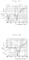
- the characteristic of absorbing the electromagnetic wave in the electromagnetic-wave absorber 1 according to the present invention is - 20 dB or more in damping factor, it is allowable that the damping factor may be - 14 dB or more when the absorber 1 is used for radio darkrooms.
- the damping factor was - 20 dB or more, but in the band 0.427 GHz to 2 GHz the damping factor was - 20 dB or less. Also, in the band 0.05 GHz to 0.71 GHz the damping factor was - 14 dB or more.
- the damping factor was - 20 dB or more. Also, in the band 0.05 GHz to 2.2 GHz, the damping factor was - 14 dB or more.
- the damping factor was - 20 dB or more. Also, in the band 0.05 GHz to 2.8 GHz, the damping factor was - 14 dB or more.
Landscapes
- Shielding Devices Or Components To Electric Or Magnetic Fields (AREA)
Applications Claiming Priority (2)
| Application Number | Priority Date | Filing Date | Title |
|---|---|---|---|
| JP28339596A JPH09219596A (ja) | 1995-11-10 | 1996-10-05 | 電磁波吸収体 |
| JP283395/96 | 1996-10-05 |
Publications (2)
| Publication Number | Publication Date |
|---|---|
| EP0828313A2 true EP0828313A2 (fr) | 1998-03-11 |
| EP0828313A3 EP0828313A3 (fr) | 1998-10-07 |
Family
ID=17664971
Family Applications (1)
| Application Number | Title | Priority Date | Filing Date |
|---|---|---|---|
| EP96308050A Withdrawn EP0828313A3 (fr) | 1996-10-05 | 1996-11-06 | Absorbant pour ondes électromagnétiques |
Country Status (1)
| Country | Link |
|---|---|
| EP (1) | EP0828313A3 (fr) |
Cited By (2)
| Publication number | Priority date | Publication date | Assignee | Title |
|---|---|---|---|---|
| RU2423761C1 (ru) * | 2010-06-07 | 2011-07-10 | Государственное образовательное учреждение высшего профессионального образования "Томский государственный университет" (ТГУ) | Способ получения многослойного радиопоглощающего материала и радиопоглощающий материал, полученный этим способом |
| DE102010055850A1 (de) | 2010-12-22 | 2012-06-28 | Deutsche Telekom Ag | Absorber für elektromagnetische Wellen |
Family Cites Families (4)
| Publication number | Priority date | Publication date | Assignee | Title |
|---|---|---|---|---|
| US3737903A (en) * | 1970-07-06 | 1973-06-05 | K Suetake | Extremely thin, wave absorptive wall |
| EP0243161B1 (fr) * | 1986-04-22 | 1992-06-24 | The Yokohama Rubber Co., Ltd. | Composé absorbant les micro-ondes |
| FR2653940B1 (fr) * | 1989-10-23 | 1992-01-10 | Commissariat Energie Atomique | Couche a anisotropie magnetique ou dielectrique et son procede de fabrication. |
| JPH04354103A (ja) * | 1991-05-31 | 1992-12-08 | Yoshiyuki Naito | 広帯域電波吸収装置 |
-
1996
- 1996-11-06 EP EP96308050A patent/EP0828313A3/fr not_active Withdrawn
Non-Patent Citations (1)
| Title |
|---|
| None |
Cited By (3)
| Publication number | Priority date | Publication date | Assignee | Title |
|---|---|---|---|---|
| RU2423761C1 (ru) * | 2010-06-07 | 2011-07-10 | Государственное образовательное учреждение высшего профессионального образования "Томский государственный университет" (ТГУ) | Способ получения многослойного радиопоглощающего материала и радиопоглощающий материал, полученный этим способом |
| DE102010055850A1 (de) | 2010-12-22 | 2012-06-28 | Deutsche Telekom Ag | Absorber für elektromagnetische Wellen |
| DE102010055850B4 (de) | 2010-12-22 | 2018-07-26 | Deutsche Telekom Ag | Absorber für elektromagnetische Wellen |
Also Published As
| Publication number | Publication date |
|---|---|
| EP0828313A3 (fr) | 1998-10-07 |
Similar Documents
| Publication | Publication Date | Title |
|---|---|---|
| US6165601A (en) | Electromagnetic-wave absorber | |
| CA1165696A (fr) | Element insonorisant | |
| EP0828313A2 (fr) | Absorbant pour ondes électromagnétiques | |
| US3871001A (en) | Radome | |
| JP2660647B2 (ja) | 電波吸収体 | |
| JP2007294903A (ja) | 遮蔽継ぎ構造および空間形成体、空間形成体を用いる試験方法 | |
| JP3509936B2 (ja) | 電波吸収材及びプレキャストコンクリート板並びにカーテンウォール | |
| US5892188A (en) | Porous ferrite wave absorber | |
| JP4004096B2 (ja) | 電波吸収体 | |
| JPH09181474A (ja) | 電磁波吸収材 | |
| KR100766836B1 (ko) | 전파 흡수 패널 | |
| Garg et al. | Airborne Sound Absorption Characteristics of Acoustical Materials for Noise Control Applications | |
| JPH10224078A (ja) | 電波吸収体 | |
| JP2853079B2 (ja) | 電波暗室 | |
| JP3244854B2 (ja) | 電波吸収壁 | |
| JPH09219596A (ja) | 電磁波吸収体 | |
| JP2003056093A (ja) | 電波吸収パネル | |
| JPH09184374A (ja) | 無線化ビル | |
| JP4222453B2 (ja) | 広帯域建材用電波吸収壁 | |
| JPH0983177A (ja) | 電波吸収パネル | |
| JP2010040640A (ja) | 電磁波遮蔽体 | |
| JP2002261489A (ja) | 電波吸収遮音パネル | |
| JP2005288969A (ja) | 積層体および薄型建築材 | |
| JPH02116199A (ja) | 電波吸収体 | |
| JPS58169998A (ja) | 複合電波吸収体 |
Legal Events
| Date | Code | Title | Description |
|---|---|---|---|
| PUAI | Public reference made under article 153(3) epc to a published international application that has entered the european phase |
Free format text: ORIGINAL CODE: 0009012 |
|
| AK | Designated contracting states |
Kind code of ref document: A2 Designated state(s): DE GB SE |
|
| PUAL | Search report despatched |
Free format text: ORIGINAL CODE: 0009013 |
|
| AK | Designated contracting states |
Kind code of ref document: A3 Designated state(s): DE GB SE |
|
| 17P | Request for examination filed |
Effective date: 19990326 |
|
| AKX | Designation fees paid |
Free format text: DE GB SE |
|
| 17Q | First examination report despatched |
Effective date: 20020719 |
|
| STAA | Information on the status of an ep patent application or granted ep patent |
Free format text: STATUS: THE APPLICATION IS DEEMED TO BE WITHDRAWN |
|
| 18D | Application deemed to be withdrawn |
Effective date: 20030130 |