EP0830650B1 - Compensation en frequence d'un regulateur a faible perte de niveau - Google Patents
Compensation en frequence d'un regulateur a faible perte de niveau Download PDFInfo
- Publication number
- EP0830650B1 EP0830650B1 EP96917251A EP96917251A EP0830650B1 EP 0830650 B1 EP0830650 B1 EP 0830650B1 EP 96917251 A EP96917251 A EP 96917251A EP 96917251 A EP96917251 A EP 96917251A EP 0830650 B1 EP0830650 B1 EP 0830650B1
- Authority
- EP
- European Patent Office
- Prior art keywords
- input
- stage
- regulator
- transistor
- output signal
- Prior art date
- Legal status (The legal status is an assumption and is not a legal conclusion. Google has not performed a legal analysis and makes no representation as to the accuracy of the status listed.)
- Expired - Lifetime
Links
- 239000003990 capacitor Substances 0.000 claims description 43
- 230000001105 regulatory effect Effects 0.000 claims description 12
- 239000000872 buffer Substances 0.000 claims description 8
- 230000003139 buffering effect Effects 0.000 claims 1
- 230000004044 response Effects 0.000 description 9
- 230000014509 gene expression Effects 0.000 description 4
- 238000013459 approach Methods 0.000 description 3
- 230000033228 biological regulation Effects 0.000 description 2
- 238000000034 method Methods 0.000 description 2
- 238000012986 modification Methods 0.000 description 2
- 230000004048 modification Effects 0.000 description 2
- 230000003071 parasitic effect Effects 0.000 description 2
- 230000010363 phase shift Effects 0.000 description 2
- 230000004913 activation Effects 0.000 description 1
- 230000001154 acute effect Effects 0.000 description 1
- 230000008859 change Effects 0.000 description 1
- 230000007423 decrease Effects 0.000 description 1
- 230000003247 decreasing effect Effects 0.000 description 1
- 230000000368 destabilizing effect Effects 0.000 description 1
- 230000000694 effects Effects 0.000 description 1
- 238000001914 filtration Methods 0.000 description 1
- 244000045947 parasite Species 0.000 description 1
- 230000006641 stabilisation Effects 0.000 description 1
Images

Classifications
-
- G—PHYSICS
- G05—CONTROLLING; REGULATING
- G05F—SYSTEMS FOR REGULATING ELECTRIC OR MAGNETIC VARIABLES
- G05F1/00—Automatic systems in which deviations of an electric quantity from one or more predetermined values are detected at the output of the system and fed back to a device within the system to restore the detected quantity to its predetermined value or values, i.e. retroactive systems
- G05F1/10—Regulating voltage or current
- G05F1/46—Regulating voltage or current wherein the variable actually regulated by the final control device is DC
- G05F1/56—Regulating voltage or current wherein the variable actually regulated by the final control device is DC using semiconductor devices in series with the load as final control devices
- G05F1/565—Regulating voltage or current wherein the variable actually regulated by the final control device is DC using semiconductor devices in series with the load as final control devices sensing a condition of the system or its load in addition to means responsive to deviations in the output of the system, e.g. current, voltage, power factor
Definitions
- This invention relates to frequency compensation in circuits, and particularly in regulator circuits.
- Low drop-out regulators i.e., regulators with a small difference between the input voltage and the regulated output voltage, and other circuits that drive a load to a voltage near one or both supply rails, can be difficult to compensate.
- Such circuits often have a large load capacitor in parallel to a load resistor. If the load capacitor is known and dependable, it can be used for part or all of the frequency compensation for the circuit. Generally, however, this capacitor is not dependable because it was not particularly selected to match the particular components of the low drop-out regulator at issue.
- ESR equivalent series resistance
- electrolytic capacitors can have an ESR ranging from many hundredths to several ohms. Even more difficult to deal with is that the ESR can increase over time. While the ESR may not interfere with filtering, it does introduce into the frequency response a zero that can stop the roll-off of the gain and can extend the bandwidth to higher frequencies at which other poles can affect the frequency response. Another consideration is that gain and loop stability are further complicated by the wide variability of resistive loads.
- Load capacitance may be addressed by indicating to users and potential users, through a product specification, that a minimum capacitance between the output terminal and ground that is required, and that this capacitor must have an ESR in a particular range. This approach, however, relies on users for proper selection of the load capacitor.
- an operational transconductance amplifier receives a feedback voltage derived from a regulator output voltage at its inverting input via a voltage divider.
- a reference voltage connects to its non-inverting input.
- the OTA compares these voltages and provides an output current to a load to equalize the feedback and reference voltages.
- a load can include a load resistor, a load capacitor C L with its inherent ESR, and even an additional current source which appears as a high impedance load.
- the transconductance (gm) of the OTA is large so that the OTA will provide the necessary load current if there is a small voltage difference at the inputs. Because an OTA will have internal poles, the unity gain frequency should be located well below the frequencies of these poles. This limitation requires any load capacitor C L to be relatively large. This is usually not a problem because there typically is a desire to make C L large enough to filter effectively against the load resistance. This remains true as long as the ESR of the load capacitor is small enough.
- Load capacitor C L causes a pole at very low frequency and the gain decreases until the reactance of C L equals the ESR. At this point, there is a zero of response, and the gain stops decreasing with increased frequency. If the ESR is greater than the reciprocal of the product of g m and an attenuation factor from the voltage divider, this zero response occurs at a frequency below the desired crossover frequency. At higher frequencies, therefore, nuisance poles of the OTA can destabilize the feedback loop.
- EP-0,531,945 discloses a low-drop voltage regulator including an operational amplifier, the regulation characteristics of the regulator being improved by providing a feedback network including a capacitive component between the output and the inverting input of the operational amplifier.
- Another approach to control regulation of the load voltage is to cascade two OTA's and provide a compensation capacitor that connects to the line between an output of the first OTA and an input to the second OTA.
- the circuit When the circuit is lightly loaded, it will have a large, finite voltage gain that is a product of the limiting gains of the OTA's.
- the gain begins to roll off at a frequency determined by load capacitor C L and by a total load resistance seen by the second OTA, including load resistance R L and any internal impedance. This result is complicated by additional poles, the most prominent of which is at the output of the first OTA. This is due to an unavoidable capacitance at the output of the first OTA and an input capacitance of the second OTA. If the two OTAs are similar, the frequencies of the two poles are near each other, thus causing the circuit to have a 40dB/decade roll-off and marginal stability.
- US-5,168,209 discloses a low drop-out regulator which includes a small internal capacitor coupled between the input of the regulator gain circuit and the base of an output transistor so as to provide AC stabilisation.
- a compensation capacitor C may be placed between the output of the first OTA and the output of the circuit to address the uncertainty about load capacitor C L and its inherent ESR. In the absence of a load capacitor C L , compensation capacitor C c may be chosen to give a unity gain frequency lower than a frequency at which other poles affect the response. If load capacitor C L is large, however, it dominates the response and can roll off the gain before some other pole appears.
- Cascaded OTA's each have poles and each requires a stable loop when used in a local feedback loop. This issue becomes a very serious problem in a low drop-out regulator in which an input section and an output device are connected to different supply rails. These regulators have problems that are not easily solved as described for the circuit referred to above.
- the output stage may include a P-type transistor, such as a PNP or PFET, connected between a supply rail and the load.
- the P-type transistor causes the regulator to pull the load positive in response to a drive pulling negative on its control electrode.
- the control signal to the control electrode may be provided by an N-type transistor that receives a control signal from an output of an OTA. This output signal is based on a difference between a reference voltage at a non-inverting input lead and a voltage based on the output signal at an inverting input.
- the invention is a low drop-out voltage regulator as set out in Claim 1.
- the present invention is a regulation-circuit that is fully frequency compensated. Accordingly. a voltage regulator has an input stage for comparing a reference voltage and an input voltage derived from the output voltage. This input state also amplifies the difference in the voltages to provide an amplified error signal. The input stage is coupled to an inverter for inverting the amplified error signal. An output stage of the voltage regulator is coupled to the inerter for providing a regulating signal at output in response to the inverted signal.
- a compensation capacitor is coupled between the output of the circuit and the output of the input stage.
- the voltage regulator circuit has an output signal that approaches one or both of the supply rails, and has a load with a load capacitor. The compensation capacitor is placed to effectively split the poles so that he gain reaches the unity gain frequency before any other poles in the system cause a phase shift of more than 180°.
- the input stage includes a differential transistor pair having an output at a drain or collector of one of the transistors.
- the inverter is a unity gain amplifier having a feedback loop that contains a feedback resistor and an equal input resistor.
- the input resistor is coupled to the collector or drain of a transistor of the differential pair.
- the output stage preferably includes an N-type transistor with its base or gate connected to the inverted signal and a collector or drain coupled to the base or gate of a P-type transistor.
- the P-type transistor has an emitter or source coupled to a supply rail.
- the load includes a load resistor in parallel with a load capacitor.
- the load may include a high impedance current source in parallel with the load resistor and load capacitor.
- the inverter between the input stage and the output stage allows the compensation capacitor to be coupled across an output terminal and an output from the comparing stage. Additional features, such as a cascode connection, may be added.
- the regulator according to the present invention is made stable without relying on a suer to provide a proper capacitance with a proper ESR.
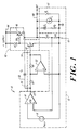
- Figure 1 is a schematic of a voltage regulator according to the present invention.
- FIG 2 is a more detailed schematic of a voltage regulator of the type shown on Figure 1.
- the present invention is a regulator circuit that is fully frequency compensated.
- the present invention is useful in the voltage regulators, and particularly in a low drop-out voltage regulator with a high impedance output stage and when regulator stages are connected stages to different supply rails.
- a low drop-out voltage regulator circuit of the present invention is frequency compensated to maintain stability without relying on the precise selection of a load capacitor. To achieve this compensation, a capacitor is coupled between an output signal of an input stage and an output of the regulator.
- low drop-out regulator 10 has a differential input stage 12, inverting stage 30, and output stage 40.
- the purpose of a regulator 10 is to receive an input voltage and to provide to a load a regulated output signal at output terminal OUT. The connection and operation of these elements will be described along with the method of providing frequency compensation.
- Regulator 10 has differential input stage 12 which has error sensing operational transconductance amplifier (OTA) 14.
- a reference voltage 16 is input to the inverting input of OTA 14.
- the input voltage signal at the non-inverting input to OTA more specifically, is derived from the output signal at output of the regulator through voltage divider 18 consisting of resistors R1 and R2.
- Inverting stage 30 is for receiving and inverting the error signal.
- Inverting stage 30 preferably includes operational amplifier (OPAMP) 32, input resistor RI, and feedback resistor RF.
- the non-inverting input of OPAMP 32 connects to ground and the inverting input connects to the error signal at the node between RI and RF.
- inverting stage 30 introduces its frequency response into the loop, inverting stage 30 preferably has a very wide bandwidth so that its poles are much higher than the unity gain frequency.
- the inverted error signal is provided on line 34 at the output of inverting stage 30
- Output stage 40 receives the inverted error signal as a control signal, and provides a regulating output signal.
- output stage preferably includes an NPN transistor Q2 at 42 with its base coupled to the output inverting stage 30.
- the collector of transistor 42 is coupled through resistor R3 to supply rail 44, and through resistor R4 to a control lead of a PNP transistor Q1 at 46.
- the emitter of transistor 42 is connected to ground.
- the emitter of PNP transistor 46 is connected to supply rail 44.
- the collector of PNP transistor 46 is coupled to output 48 of regulator 10.
- the load 47 includes, in parallel, a load resistor R L , a load capacitor C L with it inherent ESR, which is represented by R E , and current sink I L .
- Compensator capacitor C c is in line 50 that connects the output of OTA 14 and the line that connects to output 48 of the regulator (as shown in the more detailed Fig. 2, the compensator capacitor preferably is actually coupled in the OTA between a differential pair and a buffer).
- the purpose of capacitor C c is to split the poles so that the first pole associated with OTA 14 is dominated by capacitor C c , and the second pole is dominated by load capacitor C L .
- load capacitor C L causes the gain to begin to roll off.
- compensator capacitor increasingly closely couples output 48 and the output of OTA 14 in line 22.
- the compensation capacitor suppresses poles from parasitic capacitances and allows the gain to cross unity at a frequency below the destabilizing poles from these parasitic capacitances.
- FIG. 2 is a more detailed schematic of the circuit shown in Figure 1.
- a reference voltage is applied to input V ref and an error feedback to input V in of differential input stage 51.
- Input stage 51 includes transistors Q3-Q8.
- the differential output signal V O produced by differential stage transistors Q3-Q6 is buffered by transistors Q7 and Q8, which provide the buffered input stage output signal at node 62, the emitter of transistor Q8 (the output of the input stage can refer to the signal either at node 60 or at node 62).
- Transistor Q9 and resistors R5 and R6 invert the input signal and provide the inverted signal to a buffer including a Darlington follower transistor pair Q15, Q11.
- the buffered inverted signal is provided to the base of transistor Q12.
- Transistor Q10 is a load-sensitive current source that biases transistor Q11. Because the bases of transistors Q9 and Q10 are coupled together, as the signal to the base of transistor Q9 changes, it causes a corresponding change at the base of transistor Q10. Thus, transistor Q10 provides changes in current as needed to R6, and therefore transistor Qll need not fluctuate to provide current to resistor R6. Consequently, transistor Q11 serves as a more ideal buffer than it would if transistor Q10 were a constant current source. In that case, an increase at the base of transistor Q9 would cause transistor Q11 to provide more current to resistor R6. Accordingly, transistor Q11 would have to be a large current source to accommodate possible fluctuations.
- Transistor Q12 is an NPN transistor that is controlled by the inverted signal to provide, at its collector, a control signal for PNP transistor Q13.
- Transistor Q13 pulls the output of the regulator more positive when V in is less than V ref , V in is preferably derived from the output signal at 48 through a voltage divider that includes R7 and R8.
- the compensation capacitor C c is coupled from the output at 48 to a node 60 at the base of transistor Q7, and serves a function as described above.
Landscapes
- Engineering & Computer Science (AREA)
- Physics & Mathematics (AREA)
- Electromagnetism (AREA)
- General Physics & Mathematics (AREA)
- Radar, Positioning & Navigation (AREA)
- Automation & Control Theory (AREA)
- Continuous-Control Power Sources That Use Transistors (AREA)
Claims (11)
- Régulateur (10) de faible tension de relâchement pour fournir un signal de sortie régulé à une borne de sortie (OUT), comportant un étage d'entrée (12, 51) pour recevoir un signal de tension d'entrée et un signal (VREF) de tension de référence et pour fournir un signal (22, 60) de sortie d'étage d'entrée, le signal de sortie d'étage d'entrée étant fondé sur la différence entre le signal de tension d'entrée et le signal (VREF) de tension de référence, le signal de tension d'entrée étant obtenu à partir du signal de sortie régulé à la borne de sortie (OUT) ; etun étage de sortie (40, 54) non inverseur, pour fournir le signal de sortie régulé ; caractérisé en ce que le régulateur (10) comprend :un étage inverseur (30, 52) couplé à l'étage d'entrée (12, 51) pour inverser le signal de sortie d'étage d'entrée et fournir le signal de sortie inversé audit étage de sortie (40, 54) non inverseur, etun condensateur (Cc) couplé entre le signal de sortie d'étage d'entrée et le signal de sortie régulé.
- Régulateur (10) selon la revendication 1, dans lequel l'étage de sortie (40, 54) comporte un transistor d'attaque (Q2, Q12) pour recevoir le signal de sortie inversé à une borne de commande, et un transistor ballast (Q1, Q13) comportant une borne de commande et un moyen couplé au signal de sortie régulé.
- Régulateur (10) selon la revendication 2, dans lequel le transistor d'attaque (Q2, Q12) est un transistor de type n et le transistor ballast (Q1, Q13) est un transistor de type p.
- Régulateur (10) selon l'une quelconque des revendications précédentes, dans lequel l'étage inverseur (52) comporte un transistor (Q9) avec une entrée de commande, une première résistance (R5) entre l'entrée de commande et le signal de sortie d'étage d'entrée, et une deuxième résistance (R6) entre l'entrée de commande et une entrée de l'étage de sortie.
- Régulateur (10) selon la revendication 4, dans lequel lesdites première et deuxième résistances (R5, R6) ont une valeur ohmique égale et l'étage inverseur (52) a un gain unitaire.
- Régulateur (10) selon l'une quelconque des revendications précédentes, dans lequel l'étage inverseur (52) comporte une source de courant sensible à une charge et un tampon pour mémoriser en tampon le signal de sortie inverseur, la source de courant (Q10) sensible à une charge étant connectée au tampon.
- Régulateur (10) selon la revendication 6, dans lequel l'étage inverseur (52) comporte un premier transistor (Q9) qui inverse le signal de sortie d'étage d'entrée, et la source de courant sensible à une charge comporte un deuxième transistor (Q10), les bornes de commande des premier et deuxième transistors (Q9, Q10) étant couplées ensemble pour recevoir le signal de sortie d'étage d'entrée par l'intermédiaire de la première résistance (R5).
- Régulateur (10) selon la revendication 7, dans lequel le tampon comporte une paire de transistors de Darlington (Q11, Q15) ayant une borne de commande couplée au premier transistor (Q9) et une sortie couplée au deuxième transistor (Q10).
- Régulateur (10) selon la revendication 8, comportant en outre une deuxième résistance (R6) couplée entre la commande des premier et deuxième transistors (Q9, Q10) et la sortie du tampon.
- Régulateur (10) selon l'une quelconque des revendications précédentes, dans lequel le régulateur (10) comporte un diviseur de tension (R1, R2) entre le signal de sortie régulé et l'étage d'entrée (12), le signal d'entrée étant obtenu à partir du signal de sortie régulé par l'intermédiaire du diviseur de tension (R1, R2).
- Régulateur (10) selon l'une quelconque des revendications précédentes, dans lequel l'étage d'entrée (12) comporte une entrée inverseuse pour recevoir le signal (VREF) de tension de référence et une entrée non inverseuse pour recevoir le signal de tension d'entrée.
Applications Claiming Priority (3)
| Application Number | Priority Date | Filing Date | Title |
|---|---|---|---|
| US08/488,403 US5631598A (en) | 1995-06-07 | 1995-06-07 | Frequency compensation for a low drop-out regulator |
| US488403 | 1995-06-07 | ||
| PCT/US1996/009348 WO1996041248A1 (fr) | 1995-06-07 | 1996-06-05 | Compensation en frequence d'un regulateur a faible perte de niveau |
Publications (2)
| Publication Number | Publication Date |
|---|---|
| EP0830650A1 EP0830650A1 (fr) | 1998-03-25 |
| EP0830650B1 true EP0830650B1 (fr) | 1999-12-29 |
Family
ID=23939596
Family Applications (1)
| Application Number | Title | Priority Date | Filing Date |
|---|---|---|---|
| EP96917251A Expired - Lifetime EP0830650B1 (fr) | 1995-06-07 | 1996-06-05 | Compensation en frequence d'un regulateur a faible perte de niveau |
Country Status (5)
| Country | Link |
|---|---|
| US (1) | US5631598A (fr) |
| EP (1) | EP0830650B1 (fr) |
| JP (1) | JP2001507484A (fr) |
| DE (1) | DE69605915T2 (fr) |
| WO (1) | WO1996041248A1 (fr) |
Families Citing this family (69)
| Publication number | Priority date | Publication date | Assignee | Title |
|---|---|---|---|---|
| JP2000500240A (ja) * | 1996-08-29 | 2000-01-11 | フィリップス エレクトロニクス ネムローゼ フェンノートシャップ | 周波数−非依存分圧器 |
| JP3427637B2 (ja) * | 1996-09-30 | 2003-07-22 | ヤマハ株式会社 | 基準電圧発生回路 |
| FR2757711B1 (fr) * | 1996-12-19 | 2000-01-14 | Sgs Thomson Microelectronics | Dispositif de decalage de niveau |
| US5982226A (en) * | 1997-04-07 | 1999-11-09 | Texas Instruments Incorporated | Optimized frequency shaping circuit topologies for LDOs |
| US5886570A (en) * | 1997-10-22 | 1999-03-23 | Analog Devices Inc | Inverter circuit biased to limit the maximum drive current to a following stage and method |
| US5909109A (en) * | 1997-12-15 | 1999-06-01 | Cherry Semiconductor Corporation | Voltage regulator predriver circuit |
| US5929617A (en) * | 1998-03-03 | 1999-07-27 | Analog Devices, Inc. | LDO regulator dropout drive reduction circuit and method |
| US6175224B1 (en) | 1998-06-29 | 2001-01-16 | Motorola, Inc. | Regulator circuit having a bandgap generator coupled to a voltage sensor, and method |
| EP1061428B1 (fr) * | 1999-06-16 | 2005-08-31 | STMicroelectronics S.r.l. | Régulateur de tension à faible tension de déchet en technologie BICMOS / CMOS |
| US6208205B1 (en) * | 1999-07-12 | 2001-03-27 | Motorola, Inc. | Amplifier circuit and method for reducing noise therein |
| WO2001026218A1 (fr) * | 1999-10-06 | 2001-04-12 | Tripath Technology Inc. | Amplificateur a contre-reaction a gain programmable et procede servant a maintenir une phase constante |
| US6329804B1 (en) | 1999-10-13 | 2001-12-11 | National Semiconductor Corporation | Slope and level trim DAC for voltage reference |
| US6201379B1 (en) | 1999-10-13 | 2001-03-13 | National Semiconductor Corporation | CMOS voltage reference with a nulling amplifier |
| US6198266B1 (en) | 1999-10-13 | 2001-03-06 | National Semiconductor Corporation | Low dropout voltage reference |
| US6218822B1 (en) | 1999-10-13 | 2001-04-17 | National Semiconductor Corporation | CMOS voltage reference with post-assembly curvature trim |
| US6225857B1 (en) | 2000-02-08 | 2001-05-01 | Analog Devices, Inc. | Non-inverting driver circuit for low-dropout voltage regulator |
| US6304131B1 (en) * | 2000-02-22 | 2001-10-16 | Texas Instruments Incorporated | High power supply ripple rejection internally compensated low drop-out voltage regulator using PMOS pass device |
| US6201375B1 (en) | 2000-04-28 | 2001-03-13 | Burr-Brown Corporation | Overvoltage sensing and correction circuitry and method for low dropout voltage regulator |
| US6188212B1 (en) | 2000-04-28 | 2001-02-13 | Burr-Brown Corporation | Low dropout voltage regulator circuit including gate offset servo circuit powered by charge pump |
| US6300749B1 (en) * | 2000-05-02 | 2001-10-09 | Stmicroelectronics S.R.L. | Linear voltage regulator with zero mobile compensation |
| US6373233B2 (en) * | 2000-07-17 | 2002-04-16 | Philips Electronics No. America Corp. | Low-dropout voltage regulator with improved stability for all capacitive loads |
| US6414537B1 (en) * | 2000-09-12 | 2002-07-02 | National Semiconductor Corporation | Voltage reference circuit with fast disable |
| DE10054585C2 (de) * | 2000-11-03 | 2003-07-24 | Infineon Technologies Ag | Spannungsregler |
| FR2818762B1 (fr) * | 2000-12-22 | 2003-04-04 | St Microelectronics Sa | Regulateur de tension a gain statique en boucle ouverte reduit |
| WO2003012568A2 (fr) * | 2001-07-27 | 2003-02-13 | Infineon Technologies Ag | Regulateur de tension a correction de reponse en frequence |
| US6600299B2 (en) * | 2001-12-19 | 2003-07-29 | Texas Instruments Incorporated | Miller compensated NMOS low drop-out voltage regulator using variable gain stage |
| EP1336912A1 (fr) * | 2002-02-18 | 2003-08-20 | Motorola, Inc. | Régulateur de tension à faible tension de déchêt |
| US6731163B2 (en) | 2002-03-08 | 2004-05-04 | Texas Instruments Incorporated | Miller de-compensation for differential input, differential output amplifier |
| DE60335878D1 (de) | 2002-04-23 | 2011-03-10 | Nanopower Solutions Inc | Rauschfilterschaltung |
| GB2389259A (en) * | 2002-05-29 | 2003-12-03 | Zarlink Semiconductor Ltd | Amplifier and radio frequency tuner |
| US6819165B2 (en) * | 2002-05-30 | 2004-11-16 | Analog Devices, Inc. | Voltage regulator with dynamically boosted bias current |
| US6897715B2 (en) * | 2002-05-30 | 2005-05-24 | Analog Devices, Inc. | Multimode voltage regulator |
| JP3993473B2 (ja) * | 2002-06-20 | 2007-10-17 | 株式会社ルネサステクノロジ | 半導体集積回路装置 |
| DK1378808T3 (da) * | 2002-07-05 | 2008-06-23 | Dialog Semiconductor Gmbh | LDO-regulator med stort udgangsbelastningsområde og fast intern loop |
| AU2003249519A1 (en) * | 2002-08-08 | 2004-02-25 | Koninklijke Philips Electronics N.V. | Voltage regulator |
| US6989659B2 (en) * | 2002-09-09 | 2006-01-24 | Acutechnology Semiconductor | Low dropout voltage regulator using a depletion pass transistor |
| DE10249162B4 (de) * | 2002-10-22 | 2007-10-31 | Texas Instruments Deutschland Gmbh | Spannungsregler |
| US6842068B2 (en) * | 2003-02-27 | 2005-01-11 | Semiconductor Components Industries, L.L.C. | Power management method and structure |
| US6894472B2 (en) | 2003-08-20 | 2005-05-17 | Broadcom Corporation | Low leakage CMOS power mux |
| US7161339B2 (en) * | 2003-08-20 | 2007-01-09 | Broadcom Corporation | High voltage power management unit architecture in CMOS process |
| US6879142B2 (en) * | 2003-08-20 | 2005-04-12 | Broadcom Corporation | Power management unit for use in portable applications |
| US6960907B2 (en) * | 2004-02-27 | 2005-11-01 | Hitachi Global Storage Technologies Netherlands, B.V. | Efficient low dropout linear regulator |
| US7298567B2 (en) * | 2004-02-27 | 2007-11-20 | Hitachi Global Storage Technologies Netherlands B.V. | Efficient low dropout linear regulator |
| US6975099B2 (en) | 2004-02-27 | 2005-12-13 | Texas Instruments Incorporated | Efficient frequency compensation for linear voltage regulators |
| US7030595B2 (en) * | 2004-08-04 | 2006-04-18 | Nanopower Solutions Co., Ltd. | Voltage regulator having an inverse adaptive controller |
| US7245115B2 (en) * | 2005-09-07 | 2007-07-17 | Honeywell International Inc. | Low drop out voltage regulator |
| EP1947544A1 (fr) * | 2007-01-17 | 2008-07-23 | Austriamicrosystems AG | Système, dispositif, procédé et programme informatique de transfert de contenu |
| US7755338B2 (en) | 2007-07-12 | 2010-07-13 | Qimonda North America Corp. | Voltage regulator pole shifting method and apparatus |
| US7733180B1 (en) * | 2008-11-26 | 2010-06-08 | Texas Instruments Incorporated | Amplifier for driving external capacitive loads |
| US7924096B2 (en) * | 2009-03-06 | 2011-04-12 | Analog Devices, Inc. | Input buffer with impedance cancellation |
| JP2011160554A (ja) * | 2010-02-01 | 2011-08-18 | Sanyo Electric Co Ltd | 電源回路及び電子機器 |
| US8575905B2 (en) * | 2010-06-24 | 2013-11-05 | International Business Machines Corporation | Dual loop voltage regulator with bias voltage capacitor |
| FR2988184B1 (fr) * | 2012-03-15 | 2014-03-07 | St Microelectronics Rousset | Regulateur a faible chute de tension a stabilite amelioree. |
| US9223329B2 (en) * | 2013-04-18 | 2015-12-29 | Stmicroelectronics S.R.L. | Low drop out voltage regulator with operational transconductance amplifier and related method of generating a regulated voltage |
| CN104181970B (zh) * | 2014-08-29 | 2016-05-11 | 电子科技大学 | 一种内嵌基准运算放大器的低压差线性稳压器 |
| US9369099B1 (en) * | 2014-12-10 | 2016-06-14 | Qualcomm Incorporated | Low power operational transconductance amplifier |
| US9778672B1 (en) * | 2016-03-31 | 2017-10-03 | Qualcomm Incorporated | Gate boosted low drop regulator |
| KR102436699B1 (ko) * | 2016-05-11 | 2022-08-25 | 엘지전자 주식회사 | 전원공급장치, 및 이를 구비하는 영상표시장치 |
| US9946283B1 (en) * | 2016-10-18 | 2018-04-17 | Qualcomm Incorporated | Fast transient response low-dropout (LDO) regulator |
| CN108255223A (zh) * | 2016-12-28 | 2018-07-06 | 中芯国际集成电路制造(北京)有限公司 | Ldo电路 |
| US10411599B1 (en) | 2018-03-28 | 2019-09-10 | Qualcomm Incorporated | Boost and LDO hybrid converter with dual-loop control |
| US10444780B1 (en) | 2018-09-20 | 2019-10-15 | Qualcomm Incorporated | Regulation/bypass automation for LDO with multiple supply voltages |
| US10591938B1 (en) | 2018-10-16 | 2020-03-17 | Qualcomm Incorporated | PMOS-output LDO with full spectrum PSR |
| US10756676B2 (en) | 2018-10-17 | 2020-08-25 | Analog Devices Global Unlimited Company | Amplifier systems for driving a wide range of loads |
| US10545523B1 (en) | 2018-10-25 | 2020-01-28 | Qualcomm Incorporated | Adaptive gate-biased field effect transistor for low-dropout regulator |
| US10775819B2 (en) * | 2019-01-16 | 2020-09-15 | Avago Technologies International Sales Pte. Limited | Multi-loop voltage regulator with load tracking compensation |
| US11372436B2 (en) | 2019-10-14 | 2022-06-28 | Qualcomm Incorporated | Simultaneous low quiescent current and high performance LDO using single input stage and multiple output stages |
| PH12022553246A1 (en) | 2020-07-24 | 2024-02-12 | Qualcomm Inc | Charge pump based low dropout regulator |
| CN118226913A (zh) * | 2022-12-21 | 2024-06-21 | 川能电子有限公司 | 双回路线性稳压器及其稳定度补偿电路与控制方法 |
Family Cites Families (15)
| Publication number | Priority date | Publication date | Assignee | Title |
|---|---|---|---|---|
| US4356409A (en) * | 1979-06-29 | 1982-10-26 | Hitachi, Ltd. | Level conversion circuit |
| US4618832A (en) * | 1985-06-18 | 1986-10-21 | Texas Instruments Incorporated | Differential amplifier with improved power supply rejection ratio |
| NL8602409A (nl) * | 1986-09-24 | 1988-04-18 | Philips Nv | Regelbare versterker. |
| US4779037A (en) * | 1987-11-17 | 1988-10-18 | National Semiconductor Corporation | Dual input low dropout voltage regulator |
| US4908566A (en) * | 1989-02-22 | 1990-03-13 | Harris Corporation | Voltage regulator having staggered pole-zero compensation network |
| JP2888898B2 (ja) * | 1990-02-23 | 1999-05-10 | 株式会社日立製作所 | 半導体集積回路 |
| US5105102A (en) * | 1990-02-28 | 1992-04-14 | Nec Corporation | Output buffer circuit |
| US5140191A (en) * | 1990-11-05 | 1992-08-18 | Molorola, Inc. | Low di/dt BiCMOS output buffer with improved speed |
| US5168209A (en) * | 1991-06-14 | 1992-12-01 | Texas Instruments Incorporated | AC stabilization using a low frequency zero created by a small internal capacitor, such as in a low drop-out voltage regulator |
| IT1250301B (it) * | 1991-09-09 | 1995-04-07 | Sgs Thomson Microelectronics | Regolatore di tensione a bassa caduta. |
| US5191278A (en) * | 1991-10-23 | 1993-03-02 | International Business Machines Corporation | High bandwidth low dropout linear regulator |
| US5373226A (en) * | 1991-11-15 | 1994-12-13 | Nec Corporation | Constant voltage circuit formed of FETs and reference voltage generating circuit to be used therefor |
| JP3337079B2 (ja) * | 1991-11-26 | 2002-10-21 | ローム株式会社 | 電源回路 |
| US5463345A (en) * | 1993-01-07 | 1995-10-31 | Nec Corporation | Circuit for converting unipolar input to bipolar output |
| EP0661717B1 (fr) * | 1993-12-31 | 2000-03-29 | STMicroelectronics S.r.l. | Régulateur de tension pour la programmation des cellules de mémoire non volatiles, électriquement programmables |
-
1995
- 1995-06-07 US US08/488,403 patent/US5631598A/en not_active Expired - Lifetime
-
1996
- 1996-06-05 WO PCT/US1996/009348 patent/WO1996041248A1/fr not_active Ceased
- 1996-06-05 JP JP50168897A patent/JP2001507484A/ja active Pending
- 1996-06-05 DE DE69605915T patent/DE69605915T2/de not_active Expired - Lifetime
- 1996-06-05 EP EP96917251A patent/EP0830650B1/fr not_active Expired - Lifetime
Also Published As
| Publication number | Publication date |
|---|---|
| US5631598A (en) | 1997-05-20 |
| WO1996041248A1 (fr) | 1996-12-19 |
| HK1009859A1 (en) | 1999-09-03 |
| DE69605915T2 (de) | 2000-05-04 |
| EP0830650A1 (fr) | 1998-03-25 |
| DE69605915D1 (de) | 2000-02-03 |
| JP2001507484A (ja) | 2001-06-05 |
Similar Documents
| Publication | Publication Date | Title |
|---|---|---|
| EP0830650B1 (fr) | Compensation en frequence d'un regulateur a faible perte de niveau | |
| US6600299B2 (en) | Miller compensated NMOS low drop-out voltage regulator using variable gain stage | |
| US6556083B2 (en) | Method and apparatus for maintaining stability in a circuit under variable load conditions | |
| US5815012A (en) | Voltage to current converter for high frequency applications | |
| US7502719B2 (en) | Method and apparatus for overshoot and undershoot errors correction in analog low dropout regulators | |
| US4730168A (en) | CMOS output stage with large voltage swing and with stabilization of the quiescent current | |
| US6509722B2 (en) | Dynamic input stage biasing for low quiescent current amplifiers | |
| EP0777318B1 (fr) | Amplificateur opérationnel auto-compensé en fréquence | |
| US6259238B1 (en) | Brokaw transconductance operational transconductance amplifier-based micropower low drop out voltage regulator having counterphase compensation | |
| US4327319A (en) | Active power supply ripple filter | |
| JPH05250049A (ja) | 小電圧降下電圧調整器 | |
| JP2004342076A (ja) | 電圧調整器用の調整カスコード構造 | |
| JPH0588006B2 (fr) | ||
| WO1995013652A1 (fr) | Procede et appareil de compensation de frequence d'un amplificateur operationnel | |
| US6822514B1 (en) | Amplifier with miller-effect compensation for use in closed loop system such as low dropout voltage regulator | |
| JPH04273610A (ja) | 集積回路用フィルタ回路 | |
| CN115079760A (zh) | 一种低压差线性稳压器和芯片 | |
| US3538424A (en) | Voltage regulator with continuously variable dc reference | |
| US3851270A (en) | Transistorized operational amplifier | |
| US20020079935A1 (en) | Buffer/driver for low dropout regulators | |
| US4897616A (en) | Wide band amplifier with current mirror feedback to bias circuit | |
| US6933708B2 (en) | Voltage regulator with reduced open-loop static gain | |
| US4511853A (en) | Differential amplifier circuit having improved control signal filtering | |
| US4593252A (en) | Enhanced transconductance amplifier | |
| HK1009859B (en) | Frequency compensation for a low drop-out regulator |
Legal Events
| Date | Code | Title | Description |
|---|---|---|---|
| PUAI | Public reference made under article 153(3) epc to a published international application that has entered the european phase |
Free format text: ORIGINAL CODE: 0009012 |
|
| 17P | Request for examination filed |
Effective date: 19971231 |
|
| AK | Designated contracting states |
Kind code of ref document: A1 Designated state(s): DE DK FI FR GB SE |
|
| 17Q | First examination report despatched |
Effective date: 19980326 |
|
| GRAG | Despatch of communication of intention to grant |
Free format text: ORIGINAL CODE: EPIDOS AGRA |
|
| GRAG | Despatch of communication of intention to grant |
Free format text: ORIGINAL CODE: EPIDOS AGRA |
|
| GRAH | Despatch of communication of intention to grant a patent |
Free format text: ORIGINAL CODE: EPIDOS IGRA |
|
| GRAH | Despatch of communication of intention to grant a patent |
Free format text: ORIGINAL CODE: EPIDOS IGRA |
|
| GRAA | (expected) grant |
Free format text: ORIGINAL CODE: 0009210 |
|
| AK | Designated contracting states |
Kind code of ref document: B1 Designated state(s): DE DK FI FR GB SE |
|
| PG25 | Lapsed in a contracting state [announced via postgrant information from national office to epo] |
Ref country code: FI Free format text: LAPSE BECAUSE OF FAILURE TO SUBMIT A TRANSLATION OF THE DESCRIPTION OR TO PAY THE FEE WITHIN THE PRESCRIBED TIME-LIMIT Effective date: 19991229 |
|
| REF | Corresponds to: |
Ref document number: 69605915 Country of ref document: DE Date of ref document: 20000203 |
|
| ET | Fr: translation filed | ||
| PG25 | Lapsed in a contracting state [announced via postgrant information from national office to epo] |
Ref country code: DK Free format text: LAPSE BECAUSE OF FAILURE TO SUBMIT A TRANSLATION OF THE DESCRIPTION OR TO PAY THE FEE WITHIN THE PRESCRIBED TIME-LIMIT Effective date: 20000329 |
|
| PLBE | No opposition filed within time limit |
Free format text: ORIGINAL CODE: 0009261 |
|
| STAA | Information on the status of an ep patent application or granted ep patent |
Free format text: STATUS: NO OPPOSITION FILED WITHIN TIME LIMIT |
|
| 26N | No opposition filed | ||
| REG | Reference to a national code |
Ref country code: GB Ref legal event code: IF02 |
|
| PGFP | Annual fee paid to national office [announced via postgrant information from national office to epo] |
Ref country code: GB Payment date: 20140604 Year of fee payment: 19 |
|
| PGFP | Annual fee paid to national office [announced via postgrant information from national office to epo] |
Ref country code: SE Payment date: 20140611 Year of fee payment: 19 Ref country code: DE Payment date: 20140528 Year of fee payment: 19 |
|
| PGFP | Annual fee paid to national office [announced via postgrant information from national office to epo] |
Ref country code: FR Payment date: 20140609 Year of fee payment: 19 |
|
| REG | Reference to a national code |
Ref country code: DE Ref legal event code: R119 Ref document number: 69605915 Country of ref document: DE |
|
| REG | Reference to a national code |
Ref country code: SE Ref legal event code: EUG |
|
| GBPC | Gb: european patent ceased through non-payment of renewal fee |
Effective date: 20150605 |
|
| PG25 | Lapsed in a contracting state [announced via postgrant information from national office to epo] |
Ref country code: SE Free format text: LAPSE BECAUSE OF NON-PAYMENT OF DUE FEES Effective date: 20150606 |
|
| REG | Reference to a national code |
Ref country code: FR Ref legal event code: ST Effective date: 20160229 |
|
| PG25 | Lapsed in a contracting state [announced via postgrant information from national office to epo] |
Ref country code: GB Free format text: LAPSE BECAUSE OF NON-PAYMENT OF DUE FEES Effective date: 20150605 Ref country code: DE Free format text: LAPSE BECAUSE OF NON-PAYMENT OF DUE FEES Effective date: 20160101 |
|
| PG25 | Lapsed in a contracting state [announced via postgrant information from national office to epo] |
Ref country code: FR Free format text: LAPSE BECAUSE OF NON-PAYMENT OF DUE FEES Effective date: 20150630 |