EP0830736B1 - Circuit prediffuse programmable (fpga) dote d'une memoire de configuration perfectionnee et d'une table de consultation - Google Patents
Circuit prediffuse programmable (fpga) dote d'une memoire de configuration perfectionnee et d'une table de consultation Download PDFInfo
- Publication number
- EP0830736B1 EP0830736B1 EP96918446A EP96918446A EP0830736B1 EP 0830736 B1 EP0830736 B1 EP 0830736B1 EP 96918446 A EP96918446 A EP 96918446A EP 96918446 A EP96918446 A EP 96918446A EP 0830736 B1 EP0830736 B1 EP 0830736B1
- Authority
- EP
- European Patent Office
- Prior art keywords
- write
- connection
- gates
- power supply
- source
- Prior art date
- Legal status (The legal status is an assumption and is not a legal conclusion. Google has not performed a legal analysis and makes no representation as to the accuracy of the status listed.)
- Expired - Lifetime
Links
- 230000003139 buffering effect Effects 0.000 claims 1
- 239000000872 buffer Substances 0.000 description 12
- 230000009467 reduction Effects 0.000 description 3
- 238000010586 diagram Methods 0.000 description 2
- 230000002411 adverse Effects 0.000 description 1
- 230000008901 benefit Effects 0.000 description 1
- 230000008859 change Effects 0.000 description 1
- 230000006870 function Effects 0.000 description 1
- 238000000034 method Methods 0.000 description 1
- 238000012986 modification Methods 0.000 description 1
- 230000004048 modification Effects 0.000 description 1
- 230000003068 static effect Effects 0.000 description 1
Images


Classifications
-
- H—ELECTRICITY
- H03—ELECTRONIC CIRCUITRY
- H03K—PULSE TECHNIQUE
- H03K19/00—Logic circuits, i.e. having at least two inputs acting on one output; Inverting circuits
- H03K19/02—Logic circuits, i.e. having at least two inputs acting on one output; Inverting circuits using specified components
- H03K19/173—Logic circuits, i.e. having at least two inputs acting on one output; Inverting circuits using specified components using elementary logic circuits as components
- H03K19/177—Logic circuits, i.e. having at least two inputs acting on one output; Inverting circuits using specified components using elementary logic circuits as components arranged in matrix form
- H03K19/17748—Structural details of configuration resources
- H03K19/1776—Structural details of configuration resources for memories
-
- H—ELECTRICITY
- H03—ELECTRONIC CIRCUITRY
- H03K—PULSE TECHNIQUE
- H03K19/00—Logic circuits, i.e. having at least two inputs acting on one output; Inverting circuits
- H03K19/02—Logic circuits, i.e. having at least two inputs acting on one output; Inverting circuits using specified components
- H03K19/173—Logic circuits, i.e. having at least two inputs acting on one output; Inverting circuits using specified components using elementary logic circuits as components
- H03K19/177—Logic circuits, i.e. having at least two inputs acting on one output; Inverting circuits using specified components using elementary logic circuits as components arranged in matrix form
- H03K19/17704—Logic circuits, i.e. having at least two inputs acting on one output; Inverting circuits using specified components using elementary logic circuits as components arranged in matrix form the logic functions being realised by the interconnection of rows and columns
Definitions
- the present invention relates to the memory cell structure for a field programmable gate array (FPGA). More particularly, the present invention relates to reduction of components in the memory cell structure for an FPGA.
- FPGA field programmable gate array
- Fig. 1 shows a block diagram illustrating components of a typical FPGA.
- the typical FPGA includes input/output blocks (IOBs), an array of configurable logic blocks (CLBs), resources for interconnection of the CLBs, and a configuration memory.
- IOBs input/output blocks
- CLBs configurable logic blocks
- resources for interconnection of the CLBs and a configuration memory.
- the IOBs are arranged around the perimeter of the device and provide an interface between internal components of the FPGA and external package pins.
- Each of the CLBs in the array utilizes a subset of memory elements in the configuration memory as part of a look up table (LUT).
- the LUT further includes decoders (not shown) to address its memory cells. Input lines of a CLB, typically 4 or 5 lines, provide the address to the decoders.
- the LUT is programmed by storing values in its memory cells to implement Boolean functions. The memory cell of the LUT addressed provides a data bit on an output line of the CLB.
- Resources for interconnection of the CLBs include interconnect lines, programmable interconnect points (PIPs) and switching matrixes. Inputs and outputs of a CLB are connectable to other CLBs, or to an IOB utilizing the interconnect lines.
- Programmable interconnect points (PIPs) and switching matrixes connect the interconnect lines to form specific paths between CLBs, or between a CLB and an IOB.
- PIPs, as well as switching matrixes are programmed to make connections using memory cells in the configuration memory.
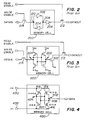
- Fig. 2 shows a typical FPGA memory cell 200 along with connections of the memory cell 200 to pass gates 212 and 214 utilized to enable reading and writing.
- the memory cell 200 is a static random access memory (SRAM) including a latch formed by inverters 202 and 204.
- a data path for signals (DATAOUT) is provided to a first end of the latch through a data path connection 208.
- a programming, or write path for signals (DATAIN) is provided to a second end of the latch through a write path connection 210.
- a CMOS Buffer 206 is provided in the data path to drive a large capacitive load without affecting the contents stored by the cell as well as to prevent cross over. Cross over occurs when two cells with data paths connected together are turned on at the same time, a condition which might affect the contents stored by a cell.
- a read enable signal is applied to pass gate 212 provided in the data path. With the read enable signal high, data can be read from the latch 202, 204.
- a write enable signal is applied to a pass gate 214 provided in the write path.
- the write enable signal high, data can be written to set or clear the latch 202, 204.
- the write enable signal high data can also be read from the write path to verify proper programming, as long as write is performed again to assure the verify operation does not disturb memory cell contents.
- Fig. 3 shows alternative to the memory cell of Fig. 2.
- the inverters 202 and 204 of Fig. 2 are provided using CMOS devices, each including a PMOS pull up transistor and an NMOS pull down transistor connected as shown.
- the CMOS buffer 206 of Fig. 2 is provided by a transistor 302 in Fig. 3 with its gate connected to the output of inverter 202, its source connected to V SS and its drain connected to pass gate 212.
- the present invention enables a reduction in the number of transistors utilized in an SRAM memory cell of an FPGA.
- the present invention further enables a reduction in the number of decoders typically utilized to control reading and writing to memory cells in an FPGA.
- the number of transistors required per memory cell may be reduced. For instance, with write performed through the data path. pass gates utilizes in a separate write path, such as pass gate 214 of Fig. 2, are not required. Further, buffers provided between the data path connection and pass gates, such as buffer 206 of Fig. 2, must be removed.
- the number of decoders previously utilized is reduced. For instance, a decoder previously utilized for controlling pass gates in the write path, such as pass gate 214, is not required. Only a decoder utilized for controlling pass gates in the data path, such as pass gate 212, will be utilized.
- transistors in the inverter of the memory cell latch driving the data path connection are made much larger than the transistors in the data path to prevent crossover and to prevent the driving of a capacitive load from disturbing latched data.
- NOR gates used to drive transistors in the data path have PMOS and NMOS transistors appropriately sized to prevent crossover.
- the present invention further includes a modified power supply.
- the modified power supply provides voltages ranging from V DD to V SS to the memory cell latch transistors during read, while providing a reduced voltage range during write to enable memory cell states to more easily be altered.
- a memory cell according to the preamble portion of Claim 1 is known from US 3 813 653 A.
- Fig. 4 shows a memory cell 400 for use with an FPGA of the present invention.
- memory cell 400 includes two inverters 402 and 404 forming a latch.
- access to memory cell 400 for both writing and reading is available only through a data path connection 408.
- the design of memory cell 400 of Fig. 4 reduces the transistor count of each memory cell from at least five in the design of Fig. 3 to four, significantly reducing overall circuitry for an FPGA.
- pass gates such as 214 of Fig. 2, previously used in a separate write path, are not required, further reducing overall circuitry for an FPGA.
- the memory cell 400 includes an inverter 402 having a PMOS pull up transistor 414 and an NMOS pull down transistor 416.
- the PMOS pull up transistor 414 has a source connected to a first power supply node 430 (V+) and a drain connected to the data path connection 408.
- the NMOS pull down transistor 416 has a source connected to a second power supply node 432 (V-), a drain connected to the data path connection 408 and a gate connected to the gate of transistor 414.
- Inverter 404 includes a PMOS pull up transistor 418 and an NMOS pull down transistor 420.
- the PMOS pull up transistor 418 has a source connected to the V+ power supply node 430 and a gate connected to the data path connection 408.
- the NMOS pull down transistor 420 has a source connected to the V- power supply node 432, a gate connected to the data path connection 408 and a drain connected to the drain of transistor 418 and to the gates of transistors 414 and 416.
- transistor sizes are adjusted to enable memory cell 400 to drive a large capacitive load, as well as to prevent cross over disturbance.
- the transistor sizes are adjusted so that the transistors of inverter 402 which drives the data path connection 408 are significantly larger than pass transistors provided in the data path. Suggested transistor sizes are shown for memory cell 400, with transistor channel width followed by channel length in microns placed next to each transistor. Transistor sizes are only suggested and may be changed to meet particular design requirements.
- Fig. 5 shows a look up table (LUT) of the present invention utilizing memory cells 500, each configured as shown in Fig. 4.
- the LUT further includes a modified power supply 502, decoder 504 and pass gates 506.
- the modified power supply 502 is utilized in the present invention to prevent a large programming voltage necessary to overcome the inverter in each memory cell which drives the data path, such as 402 of Fig. 4, from adversely affecting the pass gates 506 provided in the data path.
- the modified power supply 502 is configured to reduce the supply voltage range provided to the V+ and V- power supply nodes of each memory cell during write and increase the supply voltage range to the V+ and V-nodes during read.
- the modified power supply 502 includes first and second PMOS transistors 510 and 512, first and second NMOS transistors 514 and 516, and an inverter 518.
- the first PMOS transistor 510 has a source to drain path connecting a voltage V DD to the V+ nodes of the memory cells 500.
- the second PMOS transistor 512 has a source to drain path connecting a voltage V DD -, which has a value less than V DD , to the V+ nodes. With V DD being 5V, a suggested value for V DD - is 3.5V, although other values may be used.
- the first NMOS transistor 514 has a source to drain path connecting V SS to the V-nodes of the memory cells 500.
- the second NMOS transistor 516 has a source to drain path connecting a voltage V SS +, which has a value less than V SS , to the V- nodes. With V SS being 0V, a suggested value for V SS + is 1.5V, although other values may be used.
- the gates of transistors 510 and 516 and the input of inverter 518 receive a write/read select signal which indicates a write mode when high, and a read mode when low.
- the gates of transistors 512 and 514 receive the output of inverter 518 which provides the inverse of the write/read select signal.
- transistor 510 turns on to provide V DD to the V+ node of memory cells 500, while transistor 514 turns on to provide V SS to the V- node of memory cells 500.
- transistors 512 and 516 remain off.
- the write/read select signal is high, indicating a write mode, transistor 512 turns on to provide V DD - to the V+ node of memory cells 500, while transistor 516 turns on to provide V SS + to the V+ node of memory cells 500.
- transistors 510 and 514 remain off.
- the modified power supply 502 of the present invention pulls up V SS when V DD is reduced, an alternative configuration would only reduce V DD .
- V DD when V DD is later increased, the trip point, or thresholds of inverters of a selected memory cell, such as 402 and 404 of Fig. 4, change to possibly cause the value stored by the selected memory cell to be disturbed.
- the trip point does not deviate.
- the decoder 504 of Fig. 5 includes inverters and NOR gates, with the outputs of the NOR gates being connected to the gates of pass gates 506.
- the decoder 504 operates to decode address A0-A3 to control the gates of the pass gates 506 in the data path to enable only one of memory cells 500 at a time.
- the pass gates 506 include a first set of pass gates 520 and a second set of pass gates 522.
- Pass gates in the first set of pass gates 520 each have a source to drain path connected on a first end to a respective one of memory cells 500.
- Pass gates in the second set of pass gates 522 have a source to drain paths connected together on a first end, and a second end connected to second ends of a respective group of pass gates 520.
- Each group of pass gates in pass gates 520 is defined by including no more than one pass gate connected to a single NOR gate. Note that as defined, the first pass gates 520 include four groups as shown, each group being connected to one of pass gates in the second set of pass gates 522.
- the pass gates 506 are appropriately sized smaller than the size of transistors in the inverter of each memory cell connected to the data path to help prevent crossover disturbance during read operations.
- the NOR gates of the decoder are appropriately sized to help prevent crossover disturbance.
- the PMOS transistors are made significantly smaller than corresponding NMOS transistors to eliminate crossover and minimize downstream capacitance.
- no two pass transistors in a group of the first pass transistors 520 will be on at the same time.
- no pass transistors in the second pass transistors 522 will be on at the same time. Since a group of pass gates in 520 includes no more than one pass gate connected to a NOR gate, two of memory cells 500 transitioning states will not be connected together to create cross over.
- the NOR gates are shown with suggested channel type and transistor dimensions for their p and n channel transistors, with a p or n indicating channel type followed by channel width and length in microns.
- transistor sizes for inverter 518 are shown with a p or n indicating channel type followed by channel width and length in microns.
- transistor sizes for pass gates 506 are shown with a suggested channel width followed by channel length in microns. In Fig. 5, transistor sizes and types are only suggested and may be changed to meet particular design requirements.
- both read and write can be provided through the data path enabling the number of decoders previously utilized to be reduced. For instance, a decoder previously utilized for controlling pass gates in the write path, such as pass gate 214, is not required. Only the decoder 504 utilized for controlling pass gates in the data path is needed.
- Fig. 5 the second ends of pass gates 506 are connected together to form the input of a buffer 530 which provides read data (DATAOUT) to subsequent circuitry.
- the buffer 530 is necessary to reduce the capacitance of subsequent circuitry.
- the second ends of pass gates 506 are also connected through a pass gate 540 which receives the write signal (DATAIN).
- the write/read select signal provided to the modified power supply 502 is then provided to the gate of a pass gate 520 to enable the write signal to only be provided when the write/read select signal is high, indicating a write mode.
Landscapes
- Physics & Mathematics (AREA)
- Mathematical Physics (AREA)
- Engineering & Computer Science (AREA)
- Computer Hardware Design (AREA)
- Computing Systems (AREA)
- General Engineering & Computer Science (AREA)
- Static Random-Access Memory (AREA)
Claims (7)
- Circuit prédiffusé programmable, comprenant :des cellules de mémoire (400), chacune des cellules de mémoire comprenant une connexion d'acheminement de données (408) et une seconde connexion, chacune des cellules de mémoire comprenant :un premier inverseur (402) comprenant :un transistor de croissance de charge (414) comportant un parcours source-drain connectant une première connexion d'alimentation électrique (V+) à la connexion d'acheminement de données, et une grille connectée à la seconde connexion ; etun transistor de décroissance de charge (416) comportant un parcours source-drain connectant une seconde connexion d'alimentation électrique (V-) à la connexion d'acheminement de données , et une grille connectée à la seconde connexion ; etun second inverseur comprenant :un transistor de croissance de charge (418) comportant un parcours source-drain connectant la première connexion d'alimentation à la seconde connexion, et une grille connectée à la connexion d'acheminement de données; etun transistor de décroissance de charge (420) comportant un parcours source-drain connectant la seconde connexion d'alimentation électrique à la seconde connexion, et une grille connectée à la seconde connexion, caractérisé en ce que sont fournis en plus :
une alimentation électrique recevant un signal de sélection d'écriture et de lecture, un potentiel de tension VDD, un potentiel de tension VSS, un potentiel de tension VDD- ayant une valeur de tension inférieure au potentiel de tension VDD et un potentiel de tension VSS+ ayant une valeur de tension supérieure au potentiel de tension VSS, l'alimentation électrique comprenant :des moyens (510,512) pour fournir le potentiel de tension VDD à la première connexion d'alimentation électrique lorsque le signal de sélection de lecture/écriture indique un mode de lecture et pour fournir le potentiel de tension VDD- à la première connexion d'alimentation lorsque le signal de sélection de lecture/écriture indique un mode d'écriture ; etdes moyens (514, 516) pour fournir le potentiel de tension VSS à la première connexion d'alimentation lorsque le signal de sélection de lecture/écriture indique un mode de lecture et pour fournir le potentiel de tension VSS+ à la première connexion d'alimentation lorsque le signal de sélection de lecture/écriture indique un mode de lecture. - Circuit prédiffusé programmable selon la revendication 1 dans lequel chacune des cellules de mémoire comprend, de plus :
un circuit de passage (520) connecté à la connexion d'acheminement de données sans tampon afin de permettre aux signaux de lecture et d'écriture d'être fournis sélectivement à la connexion d'acheminement de données. - Circuit prédiffusé programmable selon la revendication 1 ou 2,dans lequel les moyens pour fournir le potentiel de tension VDD comprennent :un premier transistor PMOS (510) comportant un parcours source-drain connectant le potentiel de tension VDD à la première connexion d'alimentation électrique , et une grille connectée pour recevoir le signal de sélection de lecture/écriture ; etun second transistor PMOS (512) comportant un parcours source-drain connectant le potentiel de tension VDD- à la première connexion d'alimentation électrique, et une grille connectée pour recevoir une inversion du signal de sélection de lecture/écriture ; etdans lequel les moyens pour fournir le potentiel de tension VSS comprennent :un premier transistor NMOS (514) comportant un parcours source-drain connectant le potentiel de tension VSS à la seconde connexion d'alimentation, et une grille connectée pour recevoir le signal de sélection de lecture/écriture ; etun second transistor NMOS (516) comportant un parcours source-drain connectant le potentiel de tension VSS+ à la seconde connexion d'alimentation, et une grille connectée pour recevoir une inversion du signal de sélection de lecture/écriture.
- Circuit prédiffusé programmable selon l'une quelconque des revendications 1 à 3, comprenant, de plus :des circuits de passage (520), chaque circuit de passage comportant un parcours source-drain connectant la connexion d'acheminement de données d'au moins l'une des cellules de mémoire à un acheminement de données dans lequel les signaux de lecture et d'écriture sont fournis sélectivement ; etun décodeur (504) ayant des sorties connectées à au moins l'un des circuits de passage pour fournir sélectivement les signaux de lecture et d'écriture aux grilles des circuits de passage,dans lequel les transistors du premier inverseur présentent des dimensions supérieures à celles de transistors formant les circuits de passage.
- Circuit prédiffusé programmable selon l'une quelconque des revendications 1 à 3, comprenant, de plus :des circuits de passage, chaque circuit de passage comportant un parcours source-drain connectant la connexion d'acheminement de données d'au moins une des cellules de mémoire à un acheminement de données dans lequel les signaux de lecture et d'écriture sont fournis sélectivement ; etun décodeur ayant des sorties connectées à au moins un des circuits de passage pour fournir sélectivement les signaux de lecture et d'écriture aux grilles des circuits de passage, dans lequel le décodeur comprend des circuits ayant des dimensions de transistor établies pour éviter un croisement.
- Circuit prédiffusé programmable selon la revendication 5,dans lequel les circuits de passage comprennent :des premiers circuits de passage (520), comportant chacun un parcours source-drain connecté sur une extrémité à une cellule respective des cellules de mémoire ; etdes seconds circuits de passage (522) comportant des parcours source-drain connectés ensemble sur une première extrémité, chacun des seconds circuits de passage comportant une seconde extrémité de leur parcours source-darin connectée à une seconde extrémité des parcours source-drain d'un groupe respectif des premiers circuits de passage , etdans lequel le décodeur comprend :des premières portes NON-OU, chacune comportant une sortie connectée à un circuit de passage de chaque groupe respectif des premiers circuits passage ; etdes secondes portes NON-OU , chacune comportant une sortie connectée à l'un respectif des seconds circuits de passage, dans lequel les transistors PMOS des premières et secondes portes NON-OU présentent des dimensions inférieures à celles des transistors NMOS correspondants dans les premières et secondes portes NON-OU.
- Circuit prédiffusé programmable selon la revendication 4, comprenant, de plus :
un circuit de passage de commande d'écriture (540) comportant un parcours source-drain connectant le signal d'écriture à l'un ou à plusieurs des circuits de passage, le circuit de passage d'écriture ayant une grille connectée pour recevoir le signal de sélection de lecture/ écriture de sorte que le circuit de passage d'écriture laisse passer le signal d'écriture lorsque le signal de lecture/écriture indique un mode d'écriture.
Applications Claiming Priority (5)
| Application Number | Priority Date | Filing Date | Title |
|---|---|---|---|
| US10495P | 1995-06-09 | 1995-06-09 | |
| US104 | 1995-06-09 | ||
| US08/659,941 US5808942A (en) | 1995-06-09 | 1996-06-07 | Field programmable gate array (FPGA) having an improved configuration memory and look up table |
| PCT/US1996/009994 WO1996042141A1 (fr) | 1995-06-09 | 1996-06-07 | Circuit prediffuse programmable (fpga) dote d'une memoire de configuration perfectionnee et d'une table de consultation |
| US659941 | 1996-06-07 |
Publications (2)
| Publication Number | Publication Date |
|---|---|
| EP0830736A1 EP0830736A1 (fr) | 1998-03-25 |
| EP0830736B1 true EP0830736B1 (fr) | 2001-10-24 |
Family
ID=26667225
Family Applications (1)
| Application Number | Title | Priority Date | Filing Date |
|---|---|---|---|
| EP96918446A Expired - Lifetime EP0830736B1 (fr) | 1995-06-09 | 1996-06-07 | Circuit prediffuse programmable (fpga) dote d'une memoire de configuration perfectionnee et d'une table de consultation |
Country Status (3)
| Country | Link |
|---|---|
| US (1) | US5808942A (fr) |
| EP (1) | EP0830736B1 (fr) |
| WO (1) | WO1996042141A1 (fr) |
Families Citing this family (19)
| Publication number | Priority date | Publication date | Assignee | Title |
|---|---|---|---|---|
| US6049222A (en) * | 1997-12-30 | 2000-04-11 | Xilinx, Inc | Configuring an FPGA using embedded memory |
| US6028445A (en) * | 1997-12-30 | 2000-02-22 | Xilinx, Inc. | Decoder structure and method for FPGA configuration |
| US6172520B1 (en) * | 1997-12-30 | 2001-01-09 | Xilinx, Inc. | FPGA system with user-programmable configuration ports and method for reconfiguring the FPGA |
| JP2000223591A (ja) * | 1999-01-27 | 2000-08-11 | Sony Corp | 半導体記憶装置 |
| US6438737B1 (en) * | 2000-02-15 | 2002-08-20 | Intel Corporation | Reconfigurable logic for a computer |
| US7219325B1 (en) * | 2003-11-21 | 2007-05-15 | Xilinx, Inc. | Exploiting unused configuration memory cells |
| US7026840B1 (en) * | 2004-03-02 | 2006-04-11 | Altera Corporation | Programmable logic device |
| US7167022B1 (en) | 2004-03-25 | 2007-01-23 | Altera Corporation | Omnibus logic element including look up table based logic elements |
| US7183801B2 (en) * | 2004-09-08 | 2007-02-27 | Atmel Corporation | Programmable logic auto write-back |
| US7391236B2 (en) * | 2005-12-27 | 2008-06-24 | Altera Corporation | Distributed memory in field-programmable gate array integrated circuit devices |
| US7630228B2 (en) * | 2007-08-30 | 2009-12-08 | Intel Corporation | Methods and apparatuses for operating memory |
| US8321823B2 (en) * | 2007-10-04 | 2012-11-27 | Carnegie Mellon University | System and method for designing architecture for specified permutation and datapath circuits for permutation |
| TW201110935A (en) * | 2009-09-18 | 2011-04-01 | Univ Nat Yang Ming | Remote patient monitoring system and method thereof |
| WO2011156038A2 (fr) * | 2010-03-17 | 2011-12-15 | University Of Virginia Patent Foundation | Fpga fonctionnant sous la tension de seuil et circuits apparentés et leurs procédés |
| JP6377317B2 (ja) | 2012-05-30 | 2018-08-22 | 株式会社半導体エネルギー研究所 | プログラマブルロジックデバイス |
| TWI611419B (zh) | 2012-12-24 | 2018-01-11 | 半導體能源研究所股份有限公司 | 可程式邏輯裝置及半導體裝置 |
| JP6541376B2 (ja) | 2014-03-13 | 2019-07-10 | 株式会社半導体エネルギー研究所 | プログラマブルロジックデバイスの動作方法 |
| TWI643457B (zh) | 2014-04-25 | 2018-12-01 | 日商半導體能源研究所股份有限公司 | 半導體裝置 |
| US9286952B2 (en) | 2014-06-30 | 2016-03-15 | Lattice Semiconductor Corporation | SRAM with two-level voltage regulator |
Family Cites Families (5)
| Publication number | Priority date | Publication date | Assignee | Title |
|---|---|---|---|---|
| US3813653A (en) * | 1972-12-18 | 1974-05-28 | Rolm Corp | Memory cell with reduced voltage supply while writing |
| US4750155A (en) * | 1985-09-19 | 1988-06-07 | Xilinx, Incorporated | 5-Transistor memory cell which can be reliably read and written |
| US4796227A (en) * | 1987-03-17 | 1989-01-03 | Schlumberger Systems And Services, Inc. | Computer memory system |
| US4872141A (en) * | 1988-09-12 | 1989-10-03 | General Electric Company | Radiation hard memory cell having monocrystalline and non-monocrystalline inverters |
| JPH0654873B2 (ja) * | 1989-09-04 | 1994-07-20 | 株式会社東芝 | プログラマブル型論理装置 |
-
1996
- 1996-06-07 WO PCT/US1996/009994 patent/WO1996042141A1/fr not_active Ceased
- 1996-06-07 US US08/659,941 patent/US5808942A/en not_active Expired - Fee Related
- 1996-06-07 EP EP96918446A patent/EP0830736B1/fr not_active Expired - Lifetime
Also Published As
| Publication number | Publication date |
|---|---|
| US5808942A (en) | 1998-09-15 |
| WO1996042141A1 (fr) | 1996-12-27 |
| EP0830736A1 (fr) | 1998-03-25 |
Similar Documents
| Publication | Publication Date | Title |
|---|---|---|
| EP0830736B1 (fr) | Circuit prediffuse programmable (fpga) dote d'une memoire de configuration perfectionnee et d'une table de consultation | |
| US5986923A (en) | Method and apparatus for improving read/write stability of a single-port SRAM cell | |
| US5144582A (en) | Sram based cell for programmable logic devices | |
| US20070008804A1 (en) | High voltage wordline driver with a three stage level shifter | |
| US6664807B1 (en) | Repeater for buffering a signal on a long data line of a programmable logic device | |
| US5170373A (en) | Three transistor eeprom cell | |
| US6838924B1 (en) | Dual stage level shifter for low voltage operation | |
| US20010000653A1 (en) | Gate circuit and semiconductor circuit to process low amplitude signals, memory, processor and information processing system manufactured by use of them | |
| US20060120141A1 (en) | Configuration memory structure | |
| US8873278B1 (en) | Volatile memory elements with soft error upset immunity | |
| US5212663A (en) | Method to implement a large resettable static RAM without the large surge current | |
| US5349243A (en) | Latch controlled output driver | |
| US5764564A (en) | Write-assisted memory cell and method of operating same | |
| US7463056B1 (en) | Writeable shift register lookup table in FPGA with SRAM memory cells in lookup table reprogrammed by writing after initial configuration | |
| JPH06132747A (ja) | 半導体装置 | |
| US4800300A (en) | High-performance, CMOS latch for improved reliability | |
| US5517186A (en) | EPROM-based crossbar switch with zero standby power | |
| US4858182A (en) | High speed zero power reset circuit for CMOS memory cells | |
| US5054001A (en) | Transistor breakdown protection circuit | |
| US5315545A (en) | High-voltage five-transistor static random access memory cell | |
| KR100311973B1 (ko) | 로직 인터페이스 회로 및 이를 이용한 반도체 메모리 장치 | |
| US7142442B1 (en) | Segmented dataline scheme in a memory with enhanced full fault coverage memory cell testability | |
| US6301186B1 (en) | RAM cell with column clear | |
| US5513141A (en) | Single port register | |
| JP3550168B2 (ja) | 半導体記憶装置 |
Legal Events
| Date | Code | Title | Description |
|---|---|---|---|
| PUAI | Public reference made under article 153(3) epc to a published international application that has entered the european phase |
Free format text: ORIGINAL CODE: 0009012 |
|
| 17P | Request for examination filed |
Effective date: 19971024 |
|
| AK | Designated contracting states |
Kind code of ref document: A1 Designated state(s): GB |
|
| GRAG | Despatch of communication of intention to grant |
Free format text: ORIGINAL CODE: EPIDOS AGRA |
|
| GRAG | Despatch of communication of intention to grant |
Free format text: ORIGINAL CODE: EPIDOS AGRA |
|
| GRAH | Despatch of communication of intention to grant a patent |
Free format text: ORIGINAL CODE: EPIDOS IGRA |
|
| 17Q | First examination report despatched |
Effective date: 20000703 |
|
| GRAH | Despatch of communication of intention to grant a patent |
Free format text: ORIGINAL CODE: EPIDOS IGRA |
|
| RAP1 | Party data changed (applicant data changed or rights of an application transferred) |
Owner name: VANTIS CORPORATION |
|
| GRAA | (expected) grant |
Free format text: ORIGINAL CODE: 0009210 |
|
| AK | Designated contracting states |
Kind code of ref document: B1 Designated state(s): GB |
|
| REG | Reference to a national code |
Ref country code: GB Ref legal event code: IF02 |
|
| PG25 | Lapsed in a contracting state [announced via postgrant information from national office to epo] |
Ref country code: GB Free format text: LAPSE BECAUSE OF NON-PAYMENT OF DUE FEES Effective date: 20020607 |
|
| PLBE | No opposition filed within time limit |
Free format text: ORIGINAL CODE: 0009261 |
|
| STAA | Information on the status of an ep patent application or granted ep patent |
Free format text: STATUS: NO OPPOSITION FILED WITHIN TIME LIMIT |
|
| 26N | No opposition filed | ||
| GBPC | Gb: european patent ceased through non-payment of renewal fee |
Effective date: 20020607 |