EP0831344B1 - Arrangement de deux guides d'ondes en optique integré à la surface d'un substrat - Google Patents
Arrangement de deux guides d'ondes en optique integré à la surface d'un substrat Download PDFInfo
- Publication number
- EP0831344B1 EP0831344B1 EP97114075A EP97114075A EP0831344B1 EP 0831344 B1 EP0831344 B1 EP 0831344B1 EP 97114075 A EP97114075 A EP 97114075A EP 97114075 A EP97114075 A EP 97114075A EP 0831344 B1 EP0831344 B1 EP 0831344B1
- Authority
- EP
- European Patent Office
- Prior art keywords
- waveguide
- guiding
- waveguides
- axis
- weakly
- Prior art date
- Legal status (The legal status is an assumption and is not a legal conclusion. Google has not performed a legal analysis and makes no representation as to the accuracy of the status listed.)
- Expired - Lifetime
Links
- 239000000758 substrate Substances 0.000 title claims description 14
- 230000003287 optical effect Effects 0.000 claims description 17
- 230000008878 coupling Effects 0.000 claims description 7
- 238000010168 coupling process Methods 0.000 claims description 7
- 238000005859 coupling reaction Methods 0.000 claims description 7
- 239000010410 layer Substances 0.000 description 37
- 238000005253 cladding Methods 0.000 description 17
- 239000012792 core layer Substances 0.000 description 9
- 238000005516 engineering process Methods 0.000 description 2
- 230000005855 radiation Effects 0.000 description 2
- 239000002356 single layer Substances 0.000 description 2
- 230000015572 biosynthetic process Effects 0.000 description 1
- 230000001419 dependent effect Effects 0.000 description 1
- 238000010586 diagram Methods 0.000 description 1
- 238000004519 manufacturing process Methods 0.000 description 1
- 230000010287 polarization Effects 0.000 description 1
Images
Classifications
-
- G—PHYSICS
- G02—OPTICS
- G02B—OPTICAL ELEMENTS, SYSTEMS OR APPARATUS
- G02B6/00—Light guides; Structural details of arrangements comprising light guides and other optical elements, e.g. couplings
- G02B6/24—Coupling light guides
- G02B6/26—Optical coupling means
-
- G—PHYSICS
- G02—OPTICS
- G02B—OPTICAL ELEMENTS, SYSTEMS OR APPARATUS
- G02B6/00—Light guides; Structural details of arrangements comprising light guides and other optical elements, e.g. couplings
- G02B6/10—Light guides; Structural details of arrangements comprising light guides and other optical elements, e.g. couplings of the optical waveguide type
- G02B6/12—Light guides; Structural details of arrangements comprising light guides and other optical elements, e.g. couplings of the optical waveguide type of the integrated circuit kind
- G02B6/122—Basic optical elements, e.g. light-guiding paths
- G02B6/1228—Tapered waveguides, e.g. integrated spot-size transformers
Definitions
- the invention relates to an arrangement of two on the surface of a substrate integrated optical waveguides according to the preamble of claim 1.
- Waveguides used to achieve compact dimensions require weak shaft guidance.
- curved optical Link waveguide is narrower for implementation Radii of curvature are strong due to the radiation that occurs Shaft guidance necessary.
- EP-A-0 285 351 an arrangement of one on the Surface of a substrate integrated, straight in places and in sections curved optical waveguide known, by the curved on the outside of a Trenches arranged in the waveguide Waveguide can be reduced.
- JP-A-03200904 describes an optical waveguide that of a straight and a curved segment is composed.
- the waveguide is a rib waveguide formed, the rib height in the curved Segment is larger than in the straight segment.
- EP-A2-0645649 a strip-shaped optical is integrated Waveguide with between the ends of the waveguide described curved longitudinal axis.
- both types of waveguide are strong and the weak leader, on a common substrate as well their low-loss coupling is realized, with the The advantage of compact dimensions of the arrangement is given.
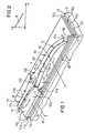
- a substrate 1 is on the surface 10 a waveguide 11 with an axis A1 and a waveguide 12 formed with an axis A2.
- the two waveguides 11 and 12 arranged coaxially one behind the other and optically coupled to each other, so that in a waveguide 11 or 12 guided wave in the other waveguide 12 or 11th can couple over.
- the axis A1 of the weakly guiding waveguide 11 is in the essentially straight and the axis A2 of the stronger leading Waveguide 12 has a curvature C with one along this axis A2 changing radius of curvature r.
- the two waveguides 11 and 12 are generally strip-like Waveguide, i.e. Waveguide, one to the surface of the substrate defined parallel and perpendicular to the axis Have width within which an optical wave in the waveguide is guided along the axis.
- An example of one strip-like waveguide is a rib waveguide.
- a ribbed waveguide (see DE 40 30 756 A1 (GR 90 P 1727 DE)) from a large area Layer waveguide, on one along an axis guided rib of predetermined width is formed.
- One in Area of the rib coupled into the layer waveguide optical wave runs along the axis of the rib and remains essentially to one defined by the width of the rib limited narrow area below the rib.
- the Axis of the rib defines the axis of the rib waveguide, along which the optical wave guided in it propagates, and the width of the fin is the width of the fin waveguide.
- both are especially weaker leading waveguide 11 as well as the stronger leading waveguide 12 each formed as a rib waveguide.
- the layer waveguide 11 0 of the weakly guiding rib waveguide 11 arranged on the flat surface 10 of the substrate 1 consists of the layers 11 1 , 11 2 and 11 3 .
- the rib 11 4 of this waveguide 11 is formed on the top layer 11 3 of the layer waveguide 11 0 and extends along the straight axis A1.
- the layer waveguide 12 0 of the stronger leading rib waveguide 12 arranged on the surface 10 of the substrate 1 consists of the layers 12 1 , 12 2 and 12 3 .
- the rib 12 4 of this waveguide 12 is formed on the uppermost layer 12 3 of the layer waveguide 12 0 and extends along the axis A2.
- the layers 11 1 and 11 3 of the layer waveguide 11 0 are cladding layers, the layer 11 2 of the layer waveguide 11 0 arranged between these cladding layers 11 1 , 11 3 is a core layer which has a higher refractive index than the cladding layers 11 1 and 11 3 and in which the optical wave guided in the rib waveguide 11 along the axis A1 of the rib 11 4 is essentially guided.
- the layers 12 1 and 12 3 of the layer waveguide 12 0 are cladding layers
- the layer 12 2 of the layer waveguide 12 0 arranged between these cladding layers 12 1 , 12 3 is a core layer which has a higher refractive index than the cladding layers 12 1 and 12 3 and in which an optical wave guided in the rib waveguide 12 along the axis A2 of the rib 11 4 is essentially guided.
- the two layer waveguides 11 0 and 12 0 of the two waveguides 11 and 12 differ from one another only in the cladding layer 11 3 and 12 3 arranged on the respective core layer 11 2 and 12 2 , respectively differ in such a way that the thickness t2 of the cladding layer 12 3 is smaller than the thickness t1 of the cladding layer 11 3 and the height h2 of the rib 12 4 of the waveguide 12 is greater by the thickness difference t1-t2 than the height h1 of the rib 11 4 of the waveguide 11 is.
- the widths of the waveguides 11 and 12, which in the example according to FIG. 1 are specifically determined by the widths b1 and b2 of the ribs 11 4 and 12 4 , can advantageously be optimally selected independently of one another for their respective function and are therefore generally different.
- the radius of curvature r of the axis A2 of the stronger leading waveguide 12 changes so that it is in a from the weaker leading waveguide 11 pointing direction a has a continuous decrease B which is linear, so as shown in Figure 2.
- Figure 2 is the Radius of curvature r as a function of the distance from a point 0 on axis A2 pointing away from waveguide 11 Plotted in direction a.
- the two waveguides 11 and 12 are preferably optically coupled to one another by butt coupling, ie the two waveguides have directly opposite end faces 11 5 and 12 5 , which are arranged centrally to one another because of the coaxial arrangement of the two waveguides 11 and 12.
- This central arrangement has the advantage that production-related fluctuations in the width of the waveguides 11 and 12 hardly impair the coupling of a guided wave from one waveguide into the other.
- the butt coupling is advantageously realized in that the layer waveguides 11 0 and 12 0 of the two ribbed waveguides 11 and 12 are adjoining sections of a single layer waveguide assigned to both waveguides 11 and 12, the core layer of which extends over both waveguides 11 and 12 ,
- the point at which the two portions 11 0 and 12 0 adjoin each other is given by a step at which the thicker cladding layer passes over 11 3 in the thinner cladding layer 12 3, and that the opposed end faces 11 5 and 12 5 of these sections 11 0 and mark 12 0 . Because of the single layer waveguide, the end faces 11 5 and 12 5 are not really imaginary end faces.
- the butt coupling enables low-loss and polarization-independent Coupling of the optical wave from one in the other waveguide.
- the relatively stronger leader Waveguide 12 is a relatively weaker leading waveguide 11 opposite tapered end portion 120 has, which leads in the direction -a to the weaker Waveguide 11 expanded and / or if the relatively weaker leading waveguide 11 a the relatively stronger leading Waveguide 12 opposite tapered end portion 110, which in the direction a to the stronger leading Waveguide 12 expanded.
- the tapered end section preferably widens 120 of the relatively more leading waveguide 12 parallel to surface 10 of substrate 1. Also widened preferably the tapered end section 110 of the weakly guiding waveguide 11 parallel to the surface 10 of the substrate 1.
- both waveguides 11 and 12 each have a taper-shaped end section 110 or 120, which widens parallel to the surface 10 of the substrate 1 and is defined by a widening of the rib 11 4 or 12 4 of this waveguide 11 or 12 is.
Landscapes
- Physics & Mathematics (AREA)
- Engineering & Computer Science (AREA)
- General Physics & Mathematics (AREA)
- Optics & Photonics (AREA)
- Power Engineering (AREA)
- Microelectronics & Electronic Packaging (AREA)
- Optical Integrated Circuits (AREA)
Claims (7)
- Arrangement de deux guides d'ondes optiques (11, 12) intégrés à la surface (10) d'un substrat (1) et destinés à guider chacun une onde optique le long d'un axe (A1, A2) respectif, dans lequelcaractérisé en ce que le rayon de courbure (r) présente dans la direction (a) s'éloignant du guide d'ondes (11) guidant plus faiblement, une diminution (B) linéaire, continuelle.les deux guides d'ondes optiques (11, 12) sont disposés coaxialement l'un à la suite de l'autre et sont couplés mutuellement sur le plan optique, de sorte que l'onde guidée dans un guide d'ondes (11, 12) transite dans l'autre guide d'ondes (12, 11),l'un (11) des deux guides d'ondes (11, 12) guide l'onde optique de manière relativement plus faible, et l'autre (12) de manière relativement plus forte,l'axe (A1) du guide d'ondes (11) guidant plus faiblement est sensiblement rectiligne, etl'axe (A2) du guide d'ondes (12) guidant plus fortement présente une courbure (C) avec un rayon de courbure (r) variant le long de cet axe (A2),
- Arrangement selon la revendication 1, caractérisé en ce que les deux guides d'ondes (11, 12) sont couplés l'un à l'autre par un couplage jointif bout à bout (112).
- Arrangement selon la revendication 1 ou 2, caractérisé en ce que le guide d'ondes (12) guidant plus fortement présente en regard du guide d'ondes (11) guidant plus faiblement, un tronçon d'extrémité (120) de forme effilée, qui s'élargit dans la direction (-a) vers le guide d'ondes (11) guidant plus faiblement.
- Arrangement selon l'une des revendications précédentes, notamment la revendication 3, caractérisé en ce que le guide d'ondes (11) guidant plus faiblement présente en regard du guide d'ondes (12) guidant plus fortement, un tronçon d'extrémité de forme effilée, qui s'élargit dans la direction (a) vers le guide d'ondes guidant plus fortement.
- Arrangement selon la revendication 3, caractérisé en ce que le tronçon d'extrémité (120) de forme effilée du guide d'ondes (12) guidant plus fortement, s'élargit parallèlement à la surface (10) du substrat (1).
- Arrangement selon la revendication 4 ou 5, caractérisé en ce que le tronçon d'extrémité (110) de forme effilée du guide d'ondes (11) guidant plus faiblement, s'élargit parallèlement à la surface (10) du substrat (1).
- Arrangement selon l'une des revendications précédentes, caractérisé en ce que le guide d'ondes guidant plus fortement et/ou guidant plus faiblement (12, 11), est un guide d'ondes à nervure.
Applications Claiming Priority (2)
| Application Number | Priority Date | Filing Date | Title |
|---|---|---|---|
| DE19638649 | 1996-09-20 | ||
| DE19638649 | 1996-09-20 |
Publications (3)
| Publication Number | Publication Date |
|---|---|
| EP0831344A2 EP0831344A2 (fr) | 1998-03-25 |
| EP0831344A3 EP0831344A3 (fr) | 2000-12-27 |
| EP0831344B1 true EP0831344B1 (fr) | 2003-02-26 |
Family
ID=7806387
Family Applications (1)
| Application Number | Title | Priority Date | Filing Date |
|---|---|---|---|
| EP97114075A Expired - Lifetime EP0831344B1 (fr) | 1996-09-20 | 1997-08-14 | Arrangement de deux guides d'ondes en optique integré à la surface d'un substrat |
Country Status (3)
| Country | Link |
|---|---|
| US (1) | US6028973A (fr) |
| EP (1) | EP0831344B1 (fr) |
| DE (1) | DE59709377D1 (fr) |
Families Citing this family (23)
| Publication number | Priority date | Publication date | Assignee | Title |
|---|---|---|---|---|
| KR100265795B1 (ko) * | 1997-11-18 | 2000-09-15 | 윤종용 | 광도파로칩 |
| US6122299A (en) * | 1997-12-31 | 2000-09-19 | Sdl, Inc. | Angled distributed reflector optical device with enhanced light confinement |
| EP0996005A1 (fr) * | 1998-09-22 | 2000-04-26 | Akzo Nobel N.V. | Branchement de puissance amélioré |
| US6293688B1 (en) * | 1999-11-12 | 2001-09-25 | Sparkolor Corporation | Tapered optical waveguide coupler |
| US6438280B1 (en) * | 1999-12-23 | 2002-08-20 | Litton Systems, Inc. | Integrated optics chip having reduced surface wave propagation |
| AU2001231441B2 (en) * | 2000-02-15 | 2004-02-05 | Memjet Technology Limited | Consumable authentication protocol and system |
| US6782149B2 (en) * | 2001-07-26 | 2004-08-24 | Battelle Memorial Institute | Contoured electric fields and poling in polarization-independent waveguides |
| US6687425B2 (en) | 2001-07-26 | 2004-02-03 | Battelle Memorial Institute | Waveguides and devices incorporating optically functional cladding regions |
| US6795597B2 (en) * | 2002-03-15 | 2004-09-21 | Optimer Photonics, Inc. | Electrode and core arrangements for polarization-independent waveguides |
| AU2003291823A1 (en) * | 2002-11-21 | 2004-06-18 | Optimer Photonics, Inc. | Embedded electrode integrated optical devices and methods of fabrication |
| GB2395570A (en) * | 2002-11-25 | 2004-05-26 | Tsunami Photonics Ltd | Tapered waveguide element with slot for optical element |
| TWI220810B (en) * | 2003-04-30 | 2004-09-01 | Univ Nat Taiwan | High power semiconductor laser structure |
| WO2009098829A1 (fr) * | 2008-02-06 | 2009-08-13 | Nec Corporation | Guide d'ondes optique et procédé de fabrication correspondant |
| KR100927664B1 (ko) * | 2008-04-04 | 2009-11-20 | 한국전자통신연구원 | 도파로 구조체 및 배열 도파로 격자 구조체 |
| KR101204335B1 (ko) * | 2008-12-17 | 2012-11-26 | 한국전자통신연구원 | 배열 도파로 격자 구조체들을 구비하는 광 소자 칩 |
| JP5513358B2 (ja) * | 2010-02-05 | 2014-06-04 | 日東電工株式会社 | 回路付サスペンション基板 |
| WO2019108833A1 (fr) | 2017-11-30 | 2019-06-06 | The Regents Of The University Of California | Système de commutation optique à base d'éléments photoniques au silicium intégrés sur tranche et procédé de formation |
| US10391867B1 (en) | 2018-06-09 | 2019-08-27 | Nxp Aeronautics Research, Llc | Apparatus having electric-field actuated generator for powering electrical load within vicinity of powerlines |
| US11011922B2 (en) | 2018-06-09 | 2021-05-18 | Nxp Aeronautics Research, Llc | Monitoring tower with device powered using differentials in electric field strengths within vicinity of powerlines |
| WO2021101608A1 (fr) | 2019-08-26 | 2021-05-27 | Nxp Aeronautics Research, Llc | Systèmes et appareil de voies aériennes d'uav |
| KR20240031228A (ko) | 2021-05-10 | 2024-03-07 | 엔이와이이 시스템즈 아이엔씨. | 2차원 실리콘 포토닉 MEMS 스위치 어레이를 갖는 유사 모노스태틱 LiDAR |
| CN117597603A (zh) | 2021-05-19 | 2024-02-23 | 尼亚系统有限公司 | 具有微透镜阵列及集成光子开关阵列的lidar |
| WO2024201876A1 (fr) * | 2023-03-30 | 2024-10-03 | 住友大阪セメント株式会社 | Élément de guide d'ondes optique et dispositif de modulation optique l'utilisant, et dispositif de transmission optique |
Family Cites Families (9)
| Publication number | Priority date | Publication date | Assignee | Title |
|---|---|---|---|---|
| US4810049A (en) * | 1987-04-02 | 1989-03-07 | American Telephone And Telegraph Company, At&T Bell Laboratories | Reducing bend and coupling losses in integrated optical waveguides |
| GB8814366D0 (en) * | 1988-06-16 | 1988-07-20 | Marconi Gec Ltd | Integrated optic devices |
| JP2827376B2 (ja) * | 1989-12-28 | 1998-11-25 | 日本電気株式会社 | 半導体光導波路の製造方法 |
| DE4030756A1 (de) * | 1990-09-28 | 1992-04-02 | Siemens Ag | Passiver integriert optischer richtkoppler |
| US5078516A (en) * | 1990-11-06 | 1992-01-07 | Bell Communications Research, Inc. | Tapered rib waveguides |
| CA2120792C (fr) * | 1993-07-16 | 2006-05-09 | Eisuke Sasaoka | Guide de lumiere |
| EP0645649A3 (fr) * | 1993-09-23 | 1995-05-17 | Siemens Ag | Guide d'ondes courbé en optique intégré en forme de bande. |
| US5878070A (en) * | 1995-05-25 | 1999-03-02 | Northwestern University | Photonic wire microcavity light emitting devices |
| US5799119A (en) * | 1996-07-03 | 1998-08-25 | Northern Telecom Limited | Coupling of strongly and weakly guiding waveguides for compact integrated mach zehnder modulators |
-
1997
- 1997-08-14 EP EP97114075A patent/EP0831344B1/fr not_active Expired - Lifetime
- 1997-08-14 DE DE59709377T patent/DE59709377D1/de not_active Expired - Fee Related
- 1997-09-19 US US08/934,447 patent/US6028973A/en not_active Expired - Lifetime
Also Published As
| Publication number | Publication date |
|---|---|
| EP0831344A3 (fr) | 2000-12-27 |
| EP0831344A2 (fr) | 1998-03-25 |
| DE59709377D1 (de) | 2003-04-03 |
| US6028973A (en) | 2000-02-22 |
Similar Documents
| Publication | Publication Date | Title |
|---|---|---|
| EP0831344B1 (fr) | Arrangement de deux guides d'ondes en optique integré à la surface d'un substrat | |
| EP0498170B1 (fr) | Composant optique intégré pour accoupler des guides d'ondes de dimensions différentes | |
| DE69312369T2 (de) | Planarlinse und lineares Multiplexer niederer Modenanordnung | |
| DE3751124T2 (de) | Faseroptischer Modekonverter. | |
| DE69617294T2 (de) | Zweidimensionale Segmentierung eines integrierten Wellenleiters zur Modenanpassung an einer Faser | |
| DE19613701A1 (de) | Integriert optischer Feldweitentransformator | |
| DE69128866T2 (de) | Optische Schaltung mit Y-Verzweigung | |
| EP0583679B1 (fr) | Dispositif d'optique intégrée pour transformer une onde optique avec une coupe transversale relativement petite en une onde optique avec une coupe transversale plus large | |
| DE19711507A1 (de) | Optische Verzweigungs-/Kreuzungs-Wellenleiterschaltung | |
| DE3787598T2 (de) | Optischer Multi/Demultiplexer. | |
| EP0476384A1 (fr) | Réseau optique avec plusieurs bouts arrangés côte à côte pour sortie de guides d'ondes optiques | |
| DE69831765T2 (de) | Integriertes optisches Bauelement mit Polarisationseffekt | |
| DE60124195T2 (de) | Optisches Übertragungsmodul und seine Verwendung in einem optischen Übertragungssystem | |
| EP0495202B1 (fr) | Dispositif pour changer une onde optique avec un petit diamètre du mode en une onde avec un diamètre plus grand | |
| DE2905916A1 (de) | Faseroptische uebertragungsvorrichtung | |
| EP0308602A2 (fr) | Guide d'ondes optiques enterré biréfringent ou structure de tels guides d'ondes et méthode pour la fabrication d'un tel guide d'ondes ou d'une telle structure | |
| DE60307610T2 (de) | Optischer koppler | |
| EP0819264B1 (fr) | Commutateur optique numerique | |
| EP0786677B1 (fr) | Méthode d'opération d'un réseau de phase | |
| DE60218325T2 (de) | Optischer filter | |
| EP0498320B1 (fr) | Transition de guides d'ondes lumineuses | |
| DE10054370A1 (de) | Optisches Verteilerelement | |
| DE69828369T2 (de) | Geteiltes optisches Bauelement sowie kostengünstiges Verfahren zu dessen Herstellung | |
| DE60308889T2 (de) | Optischer 2 x n leistungsteiler in integrierter optik | |
| DE10253438B4 (de) | Wellenleiterkreuzung |
Legal Events
| Date | Code | Title | Description |
|---|---|---|---|
| PUAI | Public reference made under article 153(3) epc to a published international application that has entered the european phase |
Free format text: ORIGINAL CODE: 0009012 |
|
| AK | Designated contracting states |
Kind code of ref document: A2 Designated state(s): DE FR GB |
|
| PUAL | Search report despatched |
Free format text: ORIGINAL CODE: 0009013 |
|
| AK | Designated contracting states |
Kind code of ref document: A3 Designated state(s): AT BE CH DE DK ES FI FR GB GR IE IT LI LU MC NL PT SE |
|
| 17P | Request for examination filed |
Effective date: 20010620 |
|
| RAP1 | Party data changed (applicant data changed or rights of an application transferred) |
Owner name: INFINEON TECHNOLOGIES AG |
|
| 17Q | First examination report despatched |
Effective date: 20010723 |
|
| AKX | Designation fees paid |
Free format text: DE FR GB |
|
| GRAG | Despatch of communication of intention to grant |
Free format text: ORIGINAL CODE: EPIDOS AGRA |
|
| GRAG | Despatch of communication of intention to grant |
Free format text: ORIGINAL CODE: EPIDOS AGRA |
|
| GRAH | Despatch of communication of intention to grant a patent |
Free format text: ORIGINAL CODE: EPIDOS IGRA |
|
| GRAH | Despatch of communication of intention to grant a patent |
Free format text: ORIGINAL CODE: EPIDOS IGRA |
|
| GRAA | (expected) grant |
Free format text: ORIGINAL CODE: 0009210 |
|
| AK | Designated contracting states |
Designated state(s): DE FR GB |
|
| REG | Reference to a national code |
Ref country code: GB Ref legal event code: FG4D Free format text: NOT ENGLISH |
|
| REF | Corresponds to: |
Ref document number: 59709377 Country of ref document: DE Date of ref document: 20030403 Kind code of ref document: P |
|
| GBT | Gb: translation of ep patent filed (gb section 77(6)(a)/1977) |
Effective date: 20030516 |
|
| ET | Fr: translation filed | ||
| PLBE | No opposition filed within time limit |
Free format text: ORIGINAL CODE: 0009261 |
|
| STAA | Information on the status of an ep patent application or granted ep patent |
Free format text: STATUS: NO OPPOSITION FILED WITHIN TIME LIMIT |
|
| 26N | No opposition filed |
Effective date: 20031127 |
|
| PGFP | Annual fee paid to national office [announced via postgrant information from national office to epo] |
Ref country code: GB Payment date: 20050801 Year of fee payment: 9 |
|
| PGFP | Annual fee paid to national office [announced via postgrant information from national office to epo] |
Ref country code: FR Payment date: 20050812 Year of fee payment: 9 |
|
| PGFP | Annual fee paid to national office [announced via postgrant information from national office to epo] |
Ref country code: DE Payment date: 20051011 Year of fee payment: 9 |
|
| PG25 | Lapsed in a contracting state [announced via postgrant information from national office to epo] |
Ref country code: DE Free format text: LAPSE BECAUSE OF NON-PAYMENT OF DUE FEES Effective date: 20070301 |
|
| GBPC | Gb: european patent ceased through non-payment of renewal fee |
Effective date: 20060814 |
|
| REG | Reference to a national code |
Ref country code: FR Ref legal event code: ST Effective date: 20070430 |
|
| PG25 | Lapsed in a contracting state [announced via postgrant information from national office to epo] |
Ref country code: GB Free format text: LAPSE BECAUSE OF NON-PAYMENT OF DUE FEES Effective date: 20060814 |
|
| PG25 | Lapsed in a contracting state [announced via postgrant information from national office to epo] |
Ref country code: FR Free format text: LAPSE BECAUSE OF NON-PAYMENT OF DUE FEES Effective date: 20060831 |