EP0833245A1 - Schaltungsanordnung mit zwischen Registern angeordneten kombinatorischen Blöcken - Google Patents
Schaltungsanordnung mit zwischen Registern angeordneten kombinatorischen Blöcken Download PDFInfo
- Publication number
- EP0833245A1 EP0833245A1 EP97116648A EP97116648A EP0833245A1 EP 0833245 A1 EP0833245 A1 EP 0833245A1 EP 97116648 A EP97116648 A EP 97116648A EP 97116648 A EP97116648 A EP 97116648A EP 0833245 A1 EP0833245 A1 EP 0833245A1
- Authority
- EP
- European Patent Office
- Prior art keywords
- output
- kbl
- logic blocks
- register
- value
- Prior art date
- Legal status (The legal status is an assumption and is not a legal conclusion. Google has not performed a legal analysis and makes no representation as to the accuracy of the status listed.)
- Granted
Links
Images



Classifications
-
- G—PHYSICS
- G11—INFORMATION STORAGE
- G11C—STATIC STORES
- G11C11/00—Digital stores characterised by the use of particular electric or magnetic storage elements; Storage elements therefor
- G11C11/21—Digital stores characterised by the use of particular electric or magnetic storage elements; Storage elements therefor using electric elements
- G11C11/34—Digital stores characterised by the use of particular electric or magnetic storage elements; Storage elements therefor using electric elements using semiconductor devices
- G11C11/40—Digital stores characterised by the use of particular electric or magnetic storage elements; Storage elements therefor using electric elements using semiconductor devices using transistors
- G11C11/401—Digital stores characterised by the use of particular electric or magnetic storage elements; Storage elements therefor using electric elements using semiconductor devices using transistors forming cells needing refreshing or charge regeneration, i.e. dynamic cells
- G11C11/403—Digital stores characterised by the use of particular electric or magnetic storage elements; Storage elements therefor using electric elements using semiconductor devices using transistors forming cells needing refreshing or charge regeneration, i.e. dynamic cells with charge regeneration common to a multiplicity of memory cells, i.e. external refresh
-
- G—PHYSICS
- G06—COMPUTING OR CALCULATING; COUNTING
- G06F—ELECTRIC DIGITAL DATA PROCESSING
- G06F7/00—Methods or arrangements for processing data by operating upon the order or content of the data handled
- G06F7/38—Methods or arrangements for performing computations using exclusively denominational number representation, e.g. using binary, ternary, decimal representation
- G06F7/48—Methods or arrangements for performing computations using exclusively denominational number representation, e.g. using binary, ternary, decimal representation using non-contact-making devices, e.g. tube, solid state device; using unspecified devices
- G06F7/52—Multiplying; Dividing
- G06F7/523—Multiplying only
- G06F7/53—Multiplying only in parallel-parallel fashion, i.e. both operands being entered in parallel
-
- G—PHYSICS
- G06—COMPUTING OR CALCULATING; COUNTING
- G06F—ELECTRIC DIGITAL DATA PROCESSING
- G06F7/00—Methods or arrangements for processing data by operating upon the order or content of the data handled
- G06F7/38—Methods or arrangements for performing computations using exclusively denominational number representation, e.g. using binary, ternary, decimal representation
- G06F7/48—Methods or arrangements for performing computations using exclusively denominational number representation, e.g. using binary, ternary, decimal representation using non-contact-making devices, e.g. tube, solid state device; using unspecified devices
-
- G—PHYSICS
- G06—COMPUTING OR CALCULATING; COUNTING
- G06F—ELECTRIC DIGITAL DATA PROCESSING
- G06F9/00—Arrangements for program control, e.g. control units
- G06F9/06—Arrangements for program control, e.g. control units using stored programs, i.e. using an internal store of processing equipment to receive or retain programs
- G06F9/30—Arrangements for executing machine instructions, e.g. instruction decode
- G06F9/38—Concurrent instruction execution, e.g. pipeline or look ahead
- G06F9/3867—Concurrent instruction execution, e.g. pipeline or look ahead using instruction pipelines
- G06F9/3869—Implementation aspects, e.g. pipeline latches; pipeline synchronisation and clocking
Definitions
- German patent DE 36 06 406 C2 is one Circuit arrangement known in the combinatorial blocks are provided, whose output signals to behind these blocks switched output registers are given.
- the problem underlying the invention is to change the above circuit arrangement so that the Timing is better. This problem is according to the characteristics of claim 1 solved.
- Register RG is always a clocked memory element denotes regardless of whether it is only an execution that only stores one bit (this is also called flip-flop) or can store several bits.
- a register not only denotes a storage element, take an input value but also additionally or alternatively set a value, reset (for example JK flip-flop) or save conditionally (this is called a flip-flop / Register labeled Enable).
- reset for example JK flip-flop
- register an additional asynchronous set or reset input exhibit.
- Figure 3 illustrates the circuit arrangement with which the Time behavior can be improved.
- An analysis unit ANA the values EW of the output of the input register RG1 examined whether there is a combination of values that allows the result AW to be tapped earlier at the exit from KBL, is inserted.
- the analysis unit ANA also sets the enable signal EN at the output register RG2 is value-dependent, which means that Result rather clocked into the output register.
- the circuit arrangement can be supplemented by the Spike Filter FI unit, which is a value for these signals that can be easily and quickly can be determined from the values EW.
- the circuit arrangement can be designed such that all or only part of the inputs analyzed by the ANA unit and that all or only some of the outputs of KBL with be provided with a spike filter FI.
- FIG. 4 shows an application example of the above Invention.
- a multiplier MLT for multiplication is shown two multiplicants MULT1 and MULT2 with each two four-byte inputs and two two-byte outputs Inputs (one byte each) are with MSB, the least significant Inputs (one byte each) labeled LSB; accordingly, the higher-value outputs (two each Byte) with A-MSB and the low-order outputs (two each Byte) with A-LSB.
- the result of the multiplication is with ERG named.
- the multiplier MLT is purely combinatorial.
Landscapes
- Engineering & Computer Science (AREA)
- General Physics & Mathematics (AREA)
- Physics & Mathematics (AREA)
- Theoretical Computer Science (AREA)
- Mathematical Optimization (AREA)
- Mathematical Analysis (AREA)
- Pure & Applied Mathematics (AREA)
- Computational Mathematics (AREA)
- General Engineering & Computer Science (AREA)
- Computing Systems (AREA)
- Software Systems (AREA)
- Microelectronics & Electronic Packaging (AREA)
- Computer Hardware Design (AREA)
- Logic Circuits (AREA)
- Complex Calculations (AREA)
Abstract
Description
- Die Laufzeit/Verzögerungszeit KBL-VZ von Wertänderungen durch die kombinatorischen Blöcke KBL ist kleiner als die Taktperiode minus der Setup-Zeit Setup/Hold-VZ und minus der Signallaufzeit RG-VZ durch ein Register RG. Dies ist in Figur 1 dargestellt. Zwischen ein Eingangsregister RG1 und Ausgangsregister RG2 ist ein kombinatorischer Block KBL geschaltet. Die Register RG1 und RG2 werden mit einem Taktsignal T angesteuert.
- Die Laufzeit von Wertänderungen durch die kombinatorischen Blöcke KBL ist um einen Faktor N größer als eine Taktperiode des Taktsignales T. Das Ergebnis wird aber erst N Taktsignale später am Ausgang des Ausgangsregisters RG2 nach den kombinatorischen Blöcken KBL abgegriffen.
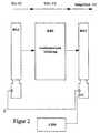
- Die Laufzeit von Wertänderungen durch die kombinatorischen Blöcke KBL ist um einen Faktor N größer als eine Taktperiode des Taktsignales T. Das Ergebnis wird aber erst N Taktsignale später in das Ausgangsregister RG2 nach den kombinatorischen Blöcken KBL eingespeichert. Dazu wird eine Enable-Anschluß EN an dem Ausgangsregister RG2 mit einem um N-Taktsignale verzögerten Impuls, erzeugt durch eine Steuerschaltung CON, angesteuert. Dies ist in Figur 2 zu sehen.
Claims (3)
- Schaltungsanordnung mit zwischen Registern (RG) angeordneten kombinatorischen Blöcken (KBL),
bei der der Ausgang des vor die kombinatorischen Blöcke (KBL) geschalteten Eingangsregisters (RG1) mit einer Analyseeinheit (ANA) verbunden ist, die den Wert (EW) des Ausgangs des Eingangsregisters (RG1) untersucht und ein Übernahmesignal(EN) für das hinter die kombinatorischen Blöcke geschaltete Ausgangsregister (RG2) abgibt, wenn der Ausgangswert (AW) der kombinatorischen Blöcke (KBL) entsprechend dem Wert (EW) des Ausgangs des Eingangsregisters (RG1) vorliegen muß. - Schaltungsanordnung nach Anspruch 1,
bei der zwischen kombinatorischen Blöcken (KBL)und Ausgangsregister (RG2) ein Spike Filter (FI) geschaltet ist. - Schaltungsanordnung nach Anspruch 1 oder 2,
bei der der kombinatorische Block (KBL) ein Multiplizierer (MLT) ist,
bei der die Analyseeinheit (ANA) dann ein Übernahmesignal (EN) abgibt, wenn die höherwertigen Stellen (MSB) der Multiplikanten (MULT1, MULT2) null sind,
bei der hinter dem Multiplizierer eine logische Schaltung angeordnet ist, der die höherwertigen Stellen (A-MSB) des Ausgangswertes des Multiplizierers für diesen Fall auf null setzt.
Applications Claiming Priority (2)
| Application Number | Priority Date | Filing Date | Title |
|---|---|---|---|
| DE19639935 | 1996-09-27 | ||
| DE19639935A DE19639935C1 (de) | 1996-09-27 | 1996-09-27 | Schaltungsanordnung mit zwischen Registern angeordneten kombinatorischen Blöcken |
Publications (2)
| Publication Number | Publication Date |
|---|---|
| EP0833245A1 true EP0833245A1 (de) | 1998-04-01 |
| EP0833245B1 EP0833245B1 (de) | 2003-02-26 |
Family
ID=7807189
Family Applications (1)
| Application Number | Title | Priority Date | Filing Date |
|---|---|---|---|
| EP97116648A Expired - Lifetime EP0833245B1 (de) | 1996-09-27 | 1997-09-24 | Schaltungsanordnung mit zwischen Registern angeordneten kombinatorischen Blöcken |
Country Status (6)
| Country | Link |
|---|---|
| US (1) | US6516334B1 (de) |
| EP (1) | EP0833245B1 (de) |
| JP (1) | JPH10149228A (de) |
| KR (1) | KR19980024848A (de) |
| DE (2) | DE19639935C1 (de) |
| TW (1) | TW419890B (de) |
Citations (3)
| Publication number | Priority date | Publication date | Assignee | Title |
|---|---|---|---|---|
| US3947671A (en) * | 1974-07-06 | 1976-03-30 | International Business Machines Corporation | Binary parallel computing arrangement for additions or subtractions |
| US4276607A (en) * | 1979-04-09 | 1981-06-30 | Sperry Rand Corporation | Multiplier circuit which detects and skips over trailing zeros |
| JPS6014325A (ja) * | 1983-07-05 | 1985-01-24 | Fuji Xerox Co Ltd | 演算回路 |
Family Cites Families (9)
| Publication number | Priority date | Publication date | Assignee | Title |
|---|---|---|---|---|
| US4460970A (en) * | 1981-05-22 | 1984-07-17 | Data General Corporation | Digital data processing system using unique techniques for handling the leading digits and the signs of operands in arithmetic operations |
| US4615016A (en) * | 1983-09-30 | 1986-09-30 | Honeywell Information Systems Inc. | Apparatus for performing simplified decimal multiplication by stripping leading zeroes |
| US4706216A (en) | 1985-02-27 | 1987-11-10 | Xilinx, Inc. | Configurable logic element |
| JPH0760990B2 (ja) * | 1989-02-23 | 1995-06-28 | エルエスアイ・ロジック株式会社 | ディジタルフィルタ |
| US5055718A (en) * | 1990-05-11 | 1991-10-08 | Actel Corporation | Logic module with configurable combinational and sequential blocks |
| DE4206082C1 (de) * | 1992-02-27 | 1993-04-08 | Siemens Ag, 8000 Muenchen, De | |
| US5262973A (en) * | 1992-03-13 | 1993-11-16 | Sun Microsystems, Inc. | Method and apparatus for optimizing complex arithmetic units for trivial operands |
| US5642306A (en) * | 1994-07-27 | 1997-06-24 | Intel Corporation | Method and apparatus for a single instruction multiple data early-out zero-skip multiplier |
| US5748516A (en) * | 1995-09-26 | 1998-05-05 | Advanced Micro Devices, Inc. | Floating point processing unit with forced arithmetic results |
-
1996
- 1996-09-27 DE DE19639935A patent/DE19639935C1/de not_active Expired - Fee Related
-
1997
- 1997-09-15 TW TW086113375A patent/TW419890B/zh not_active IP Right Cessation
- 1997-09-19 US US08/933,880 patent/US6516334B1/en not_active Expired - Fee Related
- 1997-09-23 KR KR1019970048113A patent/KR19980024848A/ko not_active Abandoned
- 1997-09-24 EP EP97116648A patent/EP0833245B1/de not_active Expired - Lifetime
- 1997-09-24 DE DE59709378T patent/DE59709378D1/de not_active Expired - Fee Related
- 1997-09-26 JP JP9261848A patent/JPH10149228A/ja active Pending
Patent Citations (3)
| Publication number | Priority date | Publication date | Assignee | Title |
|---|---|---|---|---|
| US3947671A (en) * | 1974-07-06 | 1976-03-30 | International Business Machines Corporation | Binary parallel computing arrangement for additions or subtractions |
| US4276607A (en) * | 1979-04-09 | 1981-06-30 | Sperry Rand Corporation | Multiplier circuit which detects and skips over trailing zeros |
| JPS6014325A (ja) * | 1983-07-05 | 1985-01-24 | Fuji Xerox Co Ltd | 演算回路 |
Non-Patent Citations (1)
| Title |
|---|
| PATENT ABSTRACTS OF JAPAN vol. 009, no. 129 (P - 361) 5 June 1985 (1985-06-05) * |
Also Published As
| Publication number | Publication date |
|---|---|
| JPH10149228A (ja) | 1998-06-02 |
| DE19639935C1 (de) | 1998-04-23 |
| TW419890B (en) | 2001-01-21 |
| US6516334B1 (en) | 2003-02-04 |
| KR19980024848A (ko) | 1998-07-06 |
| EP0833245B1 (de) | 2003-02-26 |
| DE59709378D1 (de) | 2003-04-03 |
Similar Documents
| Publication | Publication Date | Title |
|---|---|---|
| DE19639937C1 (de) | Schaltungsanordnung mit zwischen Registern angeordneten kombinatorischen Blöcken | |
| DE69229324T2 (de) | Arithmetik-Logik-Einheit | |
| WO1998035299A2 (de) | Verfahren zur selbstsynchronisation von konfigurierbaren elementen eines programmierbaren bausteines | |
| DE69710515T2 (de) | Verfahren und Vorrichtung zur Bestimmung von Wartezuständen auf einer Zyklusbasis in einem Datenverarbeitungssystem | |
| DE4207148A1 (de) | Superscalar-prozessor | |
| DE4434895A1 (de) | Verfahren und Vorrichtung zur Erholung von Ablaufunterbrechungen in einem Computersystem | |
| DE4403917C2 (de) | Vorrichtung zum Berechnen einer Bit-Besetzungszählung | |
| DE3700323C2 (de) | ||
| WO2009062496A1 (de) | Rekonfiguri erbare fliesskomma- und bit- ebenen datenverarbeitungseinheit | |
| DE69229840T2 (de) | Ein-Chip-Digitalprozessor und Verfahren zu seinem Betrieb | |
| DE69114328T2 (de) | Überwachung von Mikroprozessoren. | |
| DE1935944B2 (de) | Steuereinrichtung in einer elektronischen Datenverarbeitungsanlage | |
| DE69428953T2 (de) | Prioritätskodierer | |
| DE3307194C2 (de) | ||
| DE69626609T2 (de) | Pipeline-datenverarbeitungsschaltung | |
| DE2702722C2 (de) | Einrichtung zur Verarbeitung nicht direkt ausführbarer Instruktionen | |
| EP1917589B1 (de) | Verfahren und vorrichtung zum vergleich von daten bei einem rechnersystem mit wenigstens zwei ausführungseinheiten | |
| EP0833245A1 (de) | Schaltungsanordnung mit zwischen Registern angeordneten kombinatorischen Blöcken | |
| CH632349A5 (de) | Einrichtung zur mikrobefehlssteuerung. | |
| DE60201511T2 (de) | Verfahren, system und computerprogrammprodukt zum manipulieren eines anweisungsflusses in einer pipeline eines prozessors | |
| EP0305709A2 (de) | Matrix-Matrix-Multiplizierer | |
| DE69938017T2 (de) | Datenprozessor mit robuster Unterbrechungsverzweigung und Betriebsverfahren dazu | |
| DE19637369C2 (de) | Digitaler Signalprozessor mit Multipliziereinrichtung und -Verfahren | |
| DE3853256T2 (de) | Parallele Pipelinerechner. | |
| DE3851460T2 (de) | Mikrorechner. |
Legal Events
| Date | Code | Title | Description |
|---|---|---|---|
| PUAI | Public reference made under article 153(3) epc to a published international application that has entered the european phase |
Free format text: ORIGINAL CODE: 0009012 |
|
| AK | Designated contracting states |
Kind code of ref document: A1 Designated state(s): DE FR GB IT |
|
| 17P | Request for examination filed |
Effective date: 19980505 |
|
| AKX | Designation fees paid |
Free format text: DE FR GB IT |
|
| RBV | Designated contracting states (corrected) |
Designated state(s): DE FR GB IT |
|
| RAP1 | Party data changed (applicant data changed or rights of an application transferred) |
Owner name: INFINEON TECHNOLOGIES AG |
|
| 17Q | First examination report despatched |
Effective date: 20011010 |
|
| GRAG | Despatch of communication of intention to grant |
Free format text: ORIGINAL CODE: EPIDOS AGRA |
|
| GRAG | Despatch of communication of intention to grant |
Free format text: ORIGINAL CODE: EPIDOS AGRA |
|
| GRAH | Despatch of communication of intention to grant a patent |
Free format text: ORIGINAL CODE: EPIDOS IGRA |
|
| GRAH | Despatch of communication of intention to grant a patent |
Free format text: ORIGINAL CODE: EPIDOS IGRA |
|
| GRAA | (expected) grant |
Free format text: ORIGINAL CODE: 0009210 |
|
| AK | Designated contracting states |
Designated state(s): DE FR GB IT |
|
| PG25 | Lapsed in a contracting state [announced via postgrant information from national office to epo] |
Ref country code: IT Free format text: LAPSE BECAUSE OF FAILURE TO SUBMIT A TRANSLATION OF THE DESCRIPTION OR TO PAY THE FEE WITHIN THE PRE;WARNING: LAPSES OF ITALIAN PATENTS WITH EFFECTIVE DATE BEFORE 2007 MAY HAVE OCCURRED AT ANY TIME BEFORE 2007. THE CORRECT EFFECTIVE DATE MAY BE DIFFERENT FROM THE ONE RECORDED.SCRIBED TIME-LIMIT Effective date: 20030226 Ref country code: GB Free format text: LAPSE BECAUSE OF FAILURE TO SUBMIT A TRANSLATION OF THE DESCRIPTION OR TO PAY THE FEE WITHIN THE PRESCRIBED TIME-LIMIT Effective date: 20030226 Ref country code: FR Free format text: LAPSE BECAUSE OF NON-PAYMENT OF DUE FEES Effective date: 20030226 |
|
| REG | Reference to a national code |
Ref country code: GB Ref legal event code: FG4D Free format text: NOT ENGLISH |
|
| REF | Corresponds to: |
Ref document number: 59709378 Country of ref document: DE Date of ref document: 20030403 Kind code of ref document: P |
|
| GBV | Gb: ep patent (uk) treated as always having been void in accordance with gb section 77(7)/1977 [no translation filed] |
Effective date: 20030226 |
|
| PLBE | No opposition filed within time limit |
Free format text: ORIGINAL CODE: 0009261 |
|
| STAA | Information on the status of an ep patent application or granted ep patent |
Free format text: STATUS: NO OPPOSITION FILED WITHIN TIME LIMIT |
|
| EN | Fr: translation not filed | ||
| 26N | No opposition filed |
Effective date: 20031127 |
|
| PGFP | Annual fee paid to national office [announced via postgrant information from national office to epo] |
Ref country code: DE Payment date: 20061114 Year of fee payment: 10 |
|
| PG25 | Lapsed in a contracting state [announced via postgrant information from national office to epo] |
Ref country code: DE Free format text: LAPSE BECAUSE OF NON-PAYMENT OF DUE FEES Effective date: 20080401 |