EP0833342A2 - Système de mémoire et méthode de transfert de données - Google Patents
Système de mémoire et méthode de transfert de données Download PDFInfo
- Publication number
- EP0833342A2 EP0833342A2 EP97307182A EP97307182A EP0833342A2 EP 0833342 A2 EP0833342 A2 EP 0833342A2 EP 97307182 A EP97307182 A EP 97307182A EP 97307182 A EP97307182 A EP 97307182A EP 0833342 A2 EP0833342 A2 EP 0833342A2
- Authority
- EP
- European Patent Office
- Prior art keywords
- data
- memory array
- output
- bit storage
- burst
- Prior art date
- Legal status (The legal status is an assumption and is not a legal conclusion. Google has not performed a legal analysis and makes no representation as to the accuracy of the status listed.)
- Withdrawn
Links
Images


Classifications
-
- G—PHYSICS
- G06—COMPUTING OR CALCULATING; COUNTING
- G06F—ELECTRIC DIGITAL DATA PROCESSING
- G06F12/00—Accessing, addressing or allocating within memory systems or architectures
-
- G—PHYSICS
- G11—INFORMATION STORAGE
- G11C—STATIC STORES
- G11C7/00—Arrangements for writing information into, or reading information out from, a digital store
- G11C7/10—Input/output [I/O] data interface arrangements, e.g. I/O data control circuits, I/O data buffers
- G11C7/1015—Read-write modes for single port memories, i.e. having either a random port or a serial port
- G11C7/1018—Serial bit line access mode, e.g. using bit line address shift registers, bit line address counters, bit line burst counters
- G11C7/1021—Page serial bit line access mode, i.e. using an enabled row address stroke pulse with its associated word line address and a sequence of enabled column address stroke pulses each with its associated bit line address
-
- G—PHYSICS
- G11—INFORMATION STORAGE
- G11C—STATIC STORES
- G11C11/00—Digital stores characterised by the use of particular electric or magnetic storage elements; Storage elements therefor
- G11C11/21—Digital stores characterised by the use of particular electric or magnetic storage elements; Storage elements therefor using electric elements
- G11C11/34—Digital stores characterised by the use of particular electric or magnetic storage elements; Storage elements therefor using electric elements using semiconductor devices
- G11C11/40—Digital stores characterised by the use of particular electric or magnetic storage elements; Storage elements therefor using electric elements using semiconductor devices using transistors
- G11C11/401—Digital stores characterised by the use of particular electric or magnetic storage elements; Storage elements therefor using electric elements using semiconductor devices using transistors forming cells needing refreshing or charge regeneration, i.e. dynamic cells
- G11C11/4063—Auxiliary circuits, e.g. for addressing, decoding, driving, writing, sensing or timing
- G11C11/407—Auxiliary circuits, e.g. for addressing, decoding, driving, writing, sensing or timing for memory cells of the field-effect type
- G11C11/409—Read-write [R-W] circuits
- G11C11/4096—Input/output [I/O] data management or control circuits, e.g. reading or writing circuits, I/O drivers or bit-line switches
-
- G—PHYSICS
- G11—INFORMATION STORAGE
- G11C—STATIC STORES
- G11C7/00—Arrangements for writing information into, or reading information out from, a digital store
-
- G—PHYSICS
- G11—INFORMATION STORAGE
- G11C—STATIC STORES
- G11C7/00—Arrangements for writing information into, or reading information out from, a digital store
- G11C7/10—Input/output [I/O] data interface arrangements, e.g. I/O data control circuits, I/O data buffers
- G11C7/1015—Read-write modes for single port memories, i.e. having either a random port or a serial port
- G11C7/1018—Serial bit line access mode, e.g. using bit line address shift registers, bit line address counters, bit line burst counters
-
- G—PHYSICS
- G11—INFORMATION STORAGE
- G11C—STATIC STORES
- G11C7/00—Arrangements for writing information into, or reading information out from, a digital store
- G11C7/10—Input/output [I/O] data interface arrangements, e.g. I/O data control circuits, I/O data buffers
- G11C7/1051—Data output circuits, e.g. read-out amplifiers, data output buffers, data output registers, data output level conversion circuits
-
- G—PHYSICS
- G11—INFORMATION STORAGE
- G11C—STATIC STORES
- G11C7/00—Arrangements for writing information into, or reading information out from, a digital store
- G11C7/10—Input/output [I/O] data interface arrangements, e.g. I/O data control circuits, I/O data buffers
- G11C7/1075—Input/output [I/O] data interface arrangements, e.g. I/O data control circuits, I/O data buffers for multiport memories each having random access ports and serial ports, e.g. video RAM
-
- G—PHYSICS
- G11—INFORMATION STORAGE
- G11C—STATIC STORES
- G11C7/00—Arrangements for writing information into, or reading information out from, a digital store
- G11C7/10—Input/output [I/O] data interface arrangements, e.g. I/O data control circuits, I/O data buffers
- G11C7/1078—Data input circuits, e.g. write amplifiers, data input buffers, data input registers, data input level conversion circuits
- G11C7/1087—Data input latches
-
- G—PHYSICS
- G11—INFORMATION STORAGE
- G11C—STATIC STORES
- G11C7/00—Arrangements for writing information into, or reading information out from, a digital store
- G11C7/10—Input/output [I/O] data interface arrangements, e.g. I/O data control circuits, I/O data buffers
- G11C7/1078—Data input circuits, e.g. write amplifiers, data input buffers, data input registers, data input level conversion circuits
- G11C7/1093—Input synchronization
Definitions
- the present invention relates to an innovative operation and architecture for a DRAM system (a memory array system constituted by DRAMS). More specifically, the present invention relates to an innovative operation and architecture for a DRAM system that fully utilises the high-bandwidth capability and enables high speed processing.
- DRAMS are, therefore, the optimal selection for a memory device to be used in a computer system.
- the transfer speed of DRAMS (called the bandwidth, generally represented as a product of a data width and a clock rate) is slower than that of SRAMS, another memory device.
- the bandwidth of DRAMS cannot keep up with the recent enhancement of the speed of MPUs, and becomes one of the barriers to improving the performance of a computer system.
- various ideas have been provided to improve the bandwidth of DRAMS.
- Examples are synchronous DRAMS (SDRAM) and rambus DRAMS (RDRAM), which adopt a system for reading/writing consecutive address data in synchronisation with a high speed clock.
- SDRAM synchronous DRAMS
- RDRAM rambus DRAMS
- its input/output section can be operated at 100 to 250 MHz (SDRAM) or at 500 to 600 MHz (RDRAM), which is the operational speed of the clock.
- SDRAM synchronous DRAMS
- RDRAM rambus DRAMS
- an activation and precharge operation for a memory array is required for a memory array that is connected to the input/output section.
- the bandwidth of the entire memory system including the input/output section and the memory array, is drastically reduced.
- a specific value for the bandwidth can be 400 MB/s (400 MB per second).
- the bandwidth is reduced to about one third, 146 MB/s. This is due to the fact that two array activation and precharge operations are required to read/write 4-bit consecutive data, and a period equivalent to 22 clock cycles is spent for these operations.
- a high speed clock cycle of 500 MHz can not be employed effectively, and the actual operating speed is reduced to 25% to 40%.
- an extremely long time e.g., 140 ns
- the main factor related to the reduction of the bandwidth in a system is the time required for the activation and precharge operation of the memory array.
- multiple banks memory array blocks
- the activation and precharge operation for one bank is being performed while another bank is being accessed, so that the period required for the activation and precharge operation is hidden and the bandwidth is improved.
- a specific example of such a system is the SyncLink system (NIKKEI MICRODEVICES, August 1995, p.152).
- This system independently performs data reading and writing for a memory array that is divided into multiple banks. With this system, however, while a seamless operation is ensured when different banks are sequentially accessed, a seamless operation cannot be provided when the same bank is accessed continuously. This being taken into account, the average data rate is considerably reduced.
- the present inventors disclosed, in "A Full Bit Prefetch DRAMS Sensing Circuit" (IEEE JSSC, Vol. SC-31, No. 6, September 1996, pp. 762-772), a configuration whereby a full burst of read data is latched by an I/O sense amplifier by a single CAS access.
- the precharging can start two clocks before the data burst cycle begins. Since the precharging can be performed early, during the burst reading of preceding data, the subsequent RAS and CAS accesses can be performed. When eight bits are employed as a burst length, seamless reading can be performed even though the same bank is accessed. With this method, however, the seamless writing cannot be ensured.
- a prefetch mechanism is applied for writing data to separate memory array at an early stage, so that the activation and precharge operation, which must be done before reading the next set of data from the memory array, does not affect nor cause any deterioration of access speed.
- An amount of data is prefetched that is twice as much as that fetched in the period represented by an array time constant, so that in a single bank structure a seamless operation can be achieved both for reading and for writing, even when accesses to any row addresses are involved.
- a memory system comprises: a memory array consisting of multiple memory devices, an input data path for inputting external data, an output data path for externally outputting data, an input data bit storage mechanism located between the memory array and the input data path, and an output data bit storage mechanism located between the memory array and the output data path and is characterised in that data bits read from the memory array are held in the output data bit storage mechanism for external output across the output data path and an activation and prefetch operation is effected, which is required for a following data reading from the memory array.
- data bits are transferred in advance from a memory array to an output data bit storage mechanism and a first burst output is performed.
- the condition for implementing a seamless operation is the condition that exists when a sum of a RAS-CAS delay (t RCD ) and a RAS precharge time (t RP ) is smaller than a burst length (LB), i.e., t RCD + t RP ⁇ L B
- the memory array and the data input/output circuits are connected together by a latch, etc., and their operations can be separated. Further, the input circuit and the output circuit are provided separately to ensure independent operations, and reduction of the bandwidth does not occur while reading and writing are repeated alternately.
- Fig. 1 is a specific diagram illustrating one embodiment of the present invention.
- Memory arrays 1 and 2 are connected to an input circuit 20 and an output circuit 30 via a read/write latch 10.
- the input circuit 20 and the output circuit 30 are connected to external devices via a receiver and an input pin 21, and via an output buffer and an output pin 31 respectively.
- Four input latches 26, 27, 28 and 29 are provided for data input and four output latches 46, 47, 48 and 49 are provided for data output.
- These input latches are constituted by multiple input data paths 22, 23, 24 and 25, and the output latches are constituted by multiple output data paths 32, 33, 34 and 35.
- Fig. 2 is a detailed diagram illustrating the circuit shown in Fig. 1.
- the read/write latch 10 is actually separated into read latches 12 and write latches 11.
- Each set of four latches is connected to one of the data paths 22 to 25, and the data paths 32 to 35.
- sixteen write latches and sixteen read latches are distributed among 256 bit lines. In other words, one latch is provided for every 16 bit lines.
- the number of latches to be allocated for each bit line set of the 256 bit lines is determined by the time array constant and the clock frequency.
- the array time constant is 32 ns.
- the data clock frequency is 250 MHz (4ns)
- 16 latches must be provided for each bit line set of the 256 bit lines, and must prefetch to prepare for a 16-bit burst transfer.
- the arrangement in Fig. 2 is only an example acquired by employing a specific array time constant and a specific clock frequency. The present invention is not limited to the arrangement in Fig. 2.
- an activation and precharge operation for a memory array is performed while data are being latched.
- 16 bits are latched during an array time constant period of 32 ns. Every 16 ns the latches output one bit set having a 4-bit width to each of the four output data paths via read buffers 36, 37, 38 and 39, which are connected to the respective output data paths 32 to 35. And every 4 ns (250 MHz) the data are output to the exterior across the output data paths by using the output latches and the output buffers. In this manner, the 16-bit burst output can be completed within a total of 64 ns, and expression (2) can be satisfied.
- the 4-bit latches 26, 27, 28 and 29 shown in Fig. 1 are provided for input.
- the 4-bit latches drive the input data paths every 16 ns to store bit sets having a 4-bit width in the write latch 11. When all 16 bits have been stored, data writing to the memory array is performed.
- a switch RG(U) 61 or a switch RG(L) 62 goes high.
- the memory array 1 is selected.
- the switch RG(L) 62 goes high, the memory array 2 is selected.
- Fig. 3 is a timing chart in a read mode when the switch RG(U) 61 goes high. Since the switch RG(U) 61 goes high, the TRUE (T)/COMPLEMENT (C) line of a sense amplifier connected to the memory array 1 is connected to the read latch 42 across the switch RG(U) 61.
- a read latch 42 is provided for every 16 bits of the sense amplifier, and a total of sixteen bits are provided for a memory array (256 bit width).
- one of the read buffers 36, 37, 38 and 39 for external output are provided for every 64 bits, and is connected to the read latches via switch RG1, RG2, RG3 and RG4 (not shown except for the latch 42).
- a sense amplifier unit of 64-bit lines is called a block for convenience sake.
- the sense amplifier having a 256 bit width is constituted by four blocks having 64 bit widths.
- the buffers 36, 37, 38 and 39 are respectively connected to the four blocks for outputting. These buffers can increase the driving force for the output, but for them to perform the latch bit function is not inevitable.
- Each block has four read latches 42.
- the four read latches 42 are connected to one data path (e.g., the data path 32) across a connected buffer to each block and to the switches RG1, RG2, RG3 and RG4.
- the switches RG1, RG2, RG3 and RG4 go high sequentially at intervals one quarter the length of the cycle time required for the switch RG(U) to go high, as is shown by the timing chart in Fig. 3.
- the switch RG1 goes high, for example, bits stored in the read latch 42 (D1) are output externally from the buffer 36.
- the switch RG 2 goes high, and bits stored in the connecting read latch 42 (D2) are output externally from the buffer 36.
- This process is repeated for the switches RG3 and RG4, and data D3 and D4 are output externally via the buffer 36. This operation is performed for each block.
- the write mode will now be described.
- data are input in advance to the input latches 26, 27, 28 and 29 at a timing four times as fast.
- switches WG1, WG2, WG3 and WG4 go high sequentially, as is shown in Fig. 4, four bits of data are stored in the write latch 41 and in corresponding write latches (not shown) in the other blocks. More specifically, there are four blocks in the memory array and they are connected to the data paths 22, 23, 24 and 25 respectively.
- the four switches WG1, WG2, WG3 and WG4 are connected to each data path. Therefore, when the switch WG1 goes high relative to the data paths 22, 23, 24 and 25, as is shown in Fig. 4, 4 bits of data (D1) are stored in each of the four write latches.
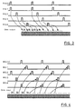
- Fig. 6 is a timing chart for explaining the operation of a DRAMS system according to the present invention, compared with a conventional SDRAM system (Fig. 5).
- the burst length for the conventional SDRAM system is four and the burst length for the DRAMS system of the present invention is sixteen, at a clock frequency for both of them is 125 MHz.
- row address R1 and column address C1 are determined by the leading edges (activation) of RAS and CAS. Based on these addresses, four data bits are output continuously in a burst mode. But when a 4-bit burst has been completed, as the activation and precharge operation for a memory array takes much time, the designation of the next row address R2 and column address C2 is delayed. Therefore, a succeeding 4-bit burst cannot be performed following a preceding 4-bit burst. That is, when the same bank is accessed, a seamless operation cannot be performed.
- the row address and the column address are designated by the leading edges of the RAS and CAS.
- Data reading begin in a 16-bit burst mode based on the first address (R1, C1).
- the 16-bit burst is performed by a read latch group that operates separately from the memory array.
- operations required for the next burst transfer such as an activation and precharge operation for a memory array, can be performed.
- These memory operations are completed when the address (R3, C3) for a following data reading is designated, because the period required for the 16-bit burst satisfies the above expression (1).
- the reading operation will not be halted. This is because the burst length that satisfies the expression (2) is employed, and because the mechanism for independently performing the reading and writing is employed.
- the read latch 11 and the write latch 12 are designed to be operated independently in order to separately perform the reading and writing operations.
- a DRAMS system that can prevent a substantial reduction in bandwidth with respect to a clock pulse frequency even when banks are accessed in no specific order.
- a memory system constituted by DRAMS whereby a seamless operation is assured not only for reading but also for writing.
Landscapes
- Engineering & Computer Science (AREA)
- Multimedia (AREA)
- Databases & Information Systems (AREA)
- Microelectronics & Electronic Packaging (AREA)
- Computer Hardware Design (AREA)
- Theoretical Computer Science (AREA)
- Physics & Mathematics (AREA)
- General Engineering & Computer Science (AREA)
- General Physics & Mathematics (AREA)
- Dram (AREA)
- Memory System (AREA)
Applications Claiming Priority (3)
| Application Number | Priority Date | Filing Date | Title |
|---|---|---|---|
| JP25712796 | 1996-09-27 | ||
| JP8257127A JPH10111828A (ja) | 1996-09-27 | 1996-09-27 | メモリシステム、データ転送方法 |
| JP257127/96 | 1996-09-27 |
Publications (2)
| Publication Number | Publication Date |
|---|---|
| EP0833342A2 true EP0833342A2 (fr) | 1998-04-01 |
| EP0833342A3 EP0833342A3 (fr) | 2005-10-26 |
Family
ID=17302110
Family Applications (1)
| Application Number | Title | Priority Date | Filing Date |
|---|---|---|---|
| EP97307182A Withdrawn EP0833342A3 (fr) | 1996-09-27 | 1997-09-16 | Système de mémoire et méthode de transfert de données |
Country Status (6)
| Country | Link |
|---|---|
| US (1) | US6085300A (fr) |
| EP (1) | EP0833342A3 (fr) |
| JP (1) | JPH10111828A (fr) |
| KR (1) | KR100268566B1 (fr) |
| SG (1) | SG77144A1 (fr) |
| TW (1) | TW325535B (fr) |
Cited By (4)
| Publication number | Priority date | Publication date | Assignee | Title |
|---|---|---|---|---|
| EP0918333A3 (fr) * | 1997-11-19 | 1999-09-15 | Fujitsu Limited | Système de transmission de signal utilisant la méthode PRD, circuit de réception pour être utilisé dans ce système de transmission de signal, et dispositif de mémoire à semiconducteurs à laquelle ce système de transmission de signal est appliquée |
| US7369444B2 (en) | 2002-06-28 | 2008-05-06 | Rambus Inc. | Early read after write operation memory device, system and method |
| US7380092B2 (en) | 2002-06-28 | 2008-05-27 | Rambus Inc. | Memory device and system having a variable depth write buffer and preload method |
| EP1532632B1 (fr) * | 2002-06-28 | 2008-10-08 | Rambus Inc. | Dispositif a memoire et systeme et procede associes permettant d'effectuer une operation de lecture rapide apres ecriture |
Families Citing this family (40)
| Publication number | Priority date | Publication date | Assignee | Title |
|---|---|---|---|---|
| US6381684B1 (en) * | 1999-04-26 | 2002-04-30 | Integrated Device Technology, Inc. | Quad data rate RAM |
| KR100372247B1 (ko) * | 2000-05-22 | 2003-02-17 | 삼성전자주식회사 | 프리페치 동작모드를 가지는 반도체 메모리 장치 및 메인데이터 라인수를 줄이기 위한 데이터 전송방법 |
| US6662319B1 (en) | 2000-08-31 | 2003-12-09 | Hewlett-Packard Development Company, L.P. | Special encoding of known bad data |
| US6671822B1 (en) * | 2000-08-31 | 2003-12-30 | Hewlett-Packard Development Company, L.P. | Method and system for absorbing defects in high performance microprocessor with a large n-way set associative cache |
| US6622225B1 (en) | 2000-08-31 | 2003-09-16 | Hewlett-Packard Development Company, L.P. | System for minimizing memory bank conflicts in a computer system |
| US6715057B1 (en) | 2000-08-31 | 2004-03-30 | Hewlett-Packard Development Company, L.P. | Efficient translation lookaside buffer miss processing in computer systems with a large range of page sizes |
| US6662265B1 (en) | 2000-08-31 | 2003-12-09 | Hewlett-Packard Development Company, L.P. | Mechanism to track all open pages in a DRAM memory system |
| US6751721B1 (en) * | 2000-08-31 | 2004-06-15 | Hewlett-Packard Development Company, L.P. | Broadcast invalidate scheme |
| US6961781B1 (en) | 2000-08-31 | 2005-11-01 | Hewlett-Packard Development Company, L.P. | Priority rules for reducing network message routing latency |
| US7213087B1 (en) | 2000-08-31 | 2007-05-01 | Hewlett-Packard Development Company, L.P. | Mechanism to control the allocation of an N-source shared buffer |
| US6567900B1 (en) | 2000-08-31 | 2003-05-20 | Hewlett-Packard Development Company, L.P. | Efficient address interleaving with simultaneous multiple locality options |
| US6633960B1 (en) * | 2000-08-31 | 2003-10-14 | Hewlett-Packard Development Company, L.P. | Scalable directory based cache coherence protocol |
| US6681295B1 (en) | 2000-08-31 | 2004-01-20 | Hewlett-Packard Development Company, L.P. | Fast lane prefetching |
| US6738836B1 (en) | 2000-08-31 | 2004-05-18 | Hewlett-Packard Development Company, L.P. | Scalable efficient I/O port protocol |
| US6654858B1 (en) | 2000-08-31 | 2003-11-25 | Hewlett-Packard Development Company, L.P. | Method for reducing directory writes and latency in a high performance, directory-based, coherency protocol |
| US6779142B1 (en) | 2000-08-31 | 2004-08-17 | Hewlett-Packard Development Company, L.P. | Apparatus and method for interfacing a high speed scan-path with slow-speed test equipment |
| US6546453B1 (en) | 2000-08-31 | 2003-04-08 | Compaq Information Technologies Group, L.P. | Proprammable DRAM address mapping mechanism |
| US6668335B1 (en) | 2000-08-31 | 2003-12-23 | Hewlett-Packard Company, L.P. | System for recovering data in a multiprocessor system comprising a conduction path for each bit between processors where the paths are grouped into separate bundles and routed along different paths |
| US6754739B1 (en) | 2000-08-31 | 2004-06-22 | Hewlett-Packard Development Company | Computer resource management and allocation system |
| US6678840B1 (en) | 2000-08-31 | 2004-01-13 | Hewlett-Packard Development Company, Lp. | Fault containment and error recovery in a scalable multiprocessor |
| US6546465B1 (en) | 2000-08-31 | 2003-04-08 | Hewlett-Packard Development Company, L.P. | Chaining directory reads and writes to reduce DRAM bandwidth in a directory based CC-NUMA protocol |
| US7099913B1 (en) | 2000-08-31 | 2006-08-29 | Hewlett-Packard Development Company, L.P. | Speculative directory writes in a directory based cache coherent nonuniform memory access protocol |
| US6636955B1 (en) | 2000-08-31 | 2003-10-21 | Hewlett-Packard Development Company, L.P. | Mechanism for synchronizing multiple skewed source-synchronous data channels with automatic initialization feature |
| US6704817B1 (en) * | 2000-08-31 | 2004-03-09 | Hewlett-Packard Development Company, L.P. | Computer architecture and system for efficient management of bi-directional bus |
| US6829682B2 (en) | 2001-04-26 | 2004-12-07 | International Business Machines Corporation | Destructive read architecture for dynamic random access memories |
| US6587388B2 (en) | 2001-04-27 | 2003-07-01 | International Business Machines Corporation | Method and apparatus for reducing write operation time in dynamic random access memories |
| US6400629B1 (en) | 2001-06-29 | 2002-06-04 | International Business Machines Corporation | System and method for early write to memory by holding bitline at fixed potential |
| US6504766B1 (en) | 2001-06-29 | 2003-01-07 | International Business Machines Corporation | System and method for early write to memory by injecting small voltage signal |
| US20030214867A1 (en) * | 2002-05-17 | 2003-11-20 | Matthew Goldman | Serially sensing the output of multilevel cell arrays |
| US6785168B2 (en) * | 2002-12-27 | 2004-08-31 | Hynix Semiconductor Inc. | Semiconductor memory device having advanced prefetch block |
| WO2005045846A1 (fr) * | 2003-11-06 | 2005-05-19 | International Business Machines Corporation | Dispositif de memoire a semi-conducteurs et procede de fonctionnement par salves de ce dernier |
| JP4370507B2 (ja) * | 2003-11-27 | 2009-11-25 | エルピーダメモリ株式会社 | 半導体集積回路装置 |
| US7748001B2 (en) * | 2004-09-23 | 2010-06-29 | Intel Corporation | Multi-thread processing system for detecting and handling live-lock conditions by arbitrating livelock priority of logical processors based on a predertermined amount of time |
| US9626194B2 (en) | 2004-09-23 | 2017-04-18 | Intel Corporation | Thread livelock unit |
| US20060143330A1 (en) * | 2004-12-23 | 2006-06-29 | Oliver Kiehl | Method for data transmit burst length control |
| TWI410970B (zh) * | 2005-07-29 | 2013-10-01 | Ibm | 控制記憶體的方法及記憶體系統 |
| JP4234126B2 (ja) | 2005-09-28 | 2009-03-04 | インターナショナル・ビジネス・マシーンズ・コーポレーション | メモリ、メモリ・アクセス制御方法 |
| US8797823B2 (en) * | 2012-10-23 | 2014-08-05 | International Business Machines Corporation | Implementing SDRAM having no RAS to CAS delay in write operation |
| US11270762B1 (en) * | 2020-08-31 | 2022-03-08 | Qualcomm Incorporated | SRAM with advanced burst mode address comparator |
| KR102918060B1 (ko) * | 2023-03-20 | 2026-01-26 | 리벨리온 주식회사 | 태스크 병렬 처리 방법 및 시스템 |
Family Cites Families (4)
| Publication number | Priority date | Publication date | Assignee | Title |
|---|---|---|---|---|
| DE3543911A1 (de) * | 1984-12-14 | 1986-06-26 | Mitsubishi Denki K.K., Tokio/Tokyo | Digitale verzoegerungseinheit |
| US5027326A (en) * | 1988-11-10 | 1991-06-25 | Dallas Semiconductor Corporation | Self-timed sequential access multiport memory |
| JP3319637B2 (ja) * | 1993-11-10 | 2002-09-03 | 松下電器産業株式会社 | 半導体記憶装置及びその制御方法 |
| WO1996020482A1 (fr) * | 1994-12-23 | 1996-07-04 | Micron Technology, Inc. | Dispositif de memoire fonctionnant en mode etendu de sortie de donnees, a acces en rafales |
-
1996
- 1996-09-27 JP JP8257127A patent/JPH10111828A/ja active Pending
-
1997
- 1997-05-29 TW TW086107341A patent/TW325535B/zh active
- 1997-07-28 KR KR1019970035511A patent/KR100268566B1/ko not_active Expired - Fee Related
- 1997-08-15 SG SG1997002951A patent/SG77144A1/en unknown
- 1997-09-16 EP EP97307182A patent/EP0833342A3/fr not_active Withdrawn
- 1997-09-19 US US08/934,034 patent/US6085300A/en not_active Expired - Lifetime
Cited By (11)
| Publication number | Priority date | Publication date | Assignee | Title |
|---|---|---|---|---|
| EP0918333A3 (fr) * | 1997-11-19 | 1999-09-15 | Fujitsu Limited | Système de transmission de signal utilisant la méthode PRD, circuit de réception pour être utilisé dans ce système de transmission de signal, et dispositif de mémoire à semiconducteurs à laquelle ce système de transmission de signal est appliquée |
| US6185256B1 (en) | 1997-11-19 | 2001-02-06 | Fujitsu Limited | Signal transmission system using PRD method, receiver circuit for use in the signal transmission system, and semiconductor memory device to which the signal transmission system is applied |
| EP1450374A1 (fr) * | 1997-11-19 | 2004-08-25 | Fujitsu Limited | Système de transmission de signal utilisant la méthode PRD, circuit de réception pour utilisation dans ce système de transmission de signal, et dispositif de mémoire à semiconducteurs auquel ce système de transmission de signal est appliqué |
| US7154797B1 (en) | 1997-11-19 | 2006-12-26 | Fujitsu Limited | Signal transmission system using PRD method, receiver circuit for use in the signal transmission system, and semiconductor memory device to which the signal transmission system is applied |
| US7505532B2 (en) | 1997-11-19 | 2009-03-17 | Fujitsu Limited | Signal transmission system using PRD method, receiver circuit for use in the signal transmission system, and semiconductor memory device to which the signal transmission system is applied |
| US7369444B2 (en) | 2002-06-28 | 2008-05-06 | Rambus Inc. | Early read after write operation memory device, system and method |
| US7380092B2 (en) | 2002-06-28 | 2008-05-27 | Rambus Inc. | Memory device and system having a variable depth write buffer and preload method |
| EP1532632B1 (fr) * | 2002-06-28 | 2008-10-08 | Rambus Inc. | Dispositif a memoire et systeme et procede associes permettant d'effectuer une operation de lecture rapide apres ecriture |
| US7848156B2 (en) | 2002-06-28 | 2010-12-07 | Rambus Inc. | Early read after write operation memory device, system and method |
| US8351281B2 (en) | 2002-06-28 | 2013-01-08 | Rambus Inc. | Early read after write operation memory device, system and method |
| US8665662B2 (en) | 2002-06-28 | 2014-03-04 | Rambus Inc. | Early read after write operation memory device, system and method |
Also Published As
| Publication number | Publication date |
|---|---|
| US6085300A (en) | 2000-07-04 |
| KR19980024110A (ko) | 1998-07-06 |
| EP0833342A3 (fr) | 2005-10-26 |
| SG77144A1 (en) | 2000-12-19 |
| JPH10111828A (ja) | 1998-04-28 |
| TW325535B (en) | 1998-01-21 |
| KR100268566B1 (ko) | 2000-10-16 |
Similar Documents
| Publication | Publication Date | Title |
|---|---|---|
| US6085300A (en) | DRAM system with simultaneous burst read and write | |
| EP0978842B1 (fr) | Dispositif de mémoire à semiconducteurs synchrone à accès à rafale | |
| US6646955B2 (en) | Synchronous dynamic random access memory | |
| US5892730A (en) | Synchronous semiconductor memory device operable in a plurality of data write operation modes | |
| JP4077874B2 (ja) | ダイナミック・ランダム・アクセス・メモリ・システム | |
| US6510492B2 (en) | Apparatus for controlling data transfer between a bus and memory array and method for operating same | |
| US6381684B1 (en) | Quad data rate RAM | |
| KR100945968B1 (ko) | 반도체기억장치 | |
| JPH09507948A (ja) | 同期式nand型dramアーキテクチャ | |
| US6252794B1 (en) | DRAM and data access method for DRAM | |
| KR0141665B1 (ko) | 비디오램 및 시리얼데이타 출력방법 | |
| US7069406B2 (en) | Double data rate synchronous SRAM with 100% bus utilization | |
| KR100652295B1 (ko) | 반도체 메모리장치 | |
| EP0520425B1 (fr) | Mémoire à semi-conducteur | |
| JP4828037B2 (ja) | 半導体メモリ装置及びデータ伝送方法 | |
| KR100326939B1 (ko) | 고속 열 사이클이 가능한 메모리의 파이프라인 구조 | |
| US6138214A (en) | Synchronous dynamic random access memory architecture for sequential burst mode | |
| US6154414A (en) | Semiconductor memory device having a plurality of memory blocks | |
| JP5028710B2 (ja) | 半導体記憶装置 | |
| JP2002237184A (ja) | 半導体記憶装置 | |
| US7230858B2 (en) | Dual frequency first-in-first-out structure | |
| EP0733259B1 (fr) | Memoire de champ amelioree | |
| JPH03238690A (ja) | 半導体メモリ回路 | |
| HK1018341A (en) | Synchronous dynamic random access memory architecture for sequential burst mode |
Legal Events
| Date | Code | Title | Description |
|---|---|---|---|
| PUAI | Public reference made under article 153(3) epc to a published international application that has entered the european phase |
Free format text: ORIGINAL CODE: 0009012 |
|
| AK | Designated contracting states |
Kind code of ref document: A2 Designated state(s): AT BE CH DE DK ES FI FR GB GR IE IT LI LU MC NL PT SE |
|
| PUAL | Search report despatched |
Free format text: ORIGINAL CODE: 0009013 |
|
| AK | Designated contracting states |
Kind code of ref document: A3 Designated state(s): AT BE CH DE DK ES FI FR GB GR IE IT LI LU MC NL PT SE |
|
| 17P | Request for examination filed |
Effective date: 20060306 |
|
| AKX | Designation fees paid |
Designated state(s): DE FR GB |
|
| 17Q | First examination report despatched |
Effective date: 20090219 |
|
| STAA | Information on the status of an ep patent application or granted ep patent |
Free format text: STATUS: THE APPLICATION IS DEEMED TO BE WITHDRAWN |
|
| 18D | Application deemed to be withdrawn |
Effective date: 20090701 |