EP0833386B1 - Dispositif semiconducteur vertical contrôlable par effet de champ - Google Patents
Dispositif semiconducteur vertical contrôlable par effet de champ Download PDFInfo
- Publication number
- EP0833386B1 EP0833386B1 EP97113580A EP97113580A EP0833386B1 EP 0833386 B1 EP0833386 B1 EP 0833386B1 EP 97113580 A EP97113580 A EP 97113580A EP 97113580 A EP97113580 A EP 97113580A EP 0833386 B1 EP0833386 B1 EP 0833386B1
- Authority
- EP
- European Patent Office
- Prior art keywords
- zones
- field effect
- source
- zone
- drain
- Prior art date
- Legal status (The legal status is an assumption and is not a legal conclusion. Google has not performed a legal analysis and makes no representation as to the accuracy of the status listed.)
- Expired - Lifetime
Links
Images
Classifications
-
- H—ELECTRICITY
- H10—SEMICONDUCTOR DEVICES; ELECTRIC SOLID-STATE DEVICES NOT OTHERWISE PROVIDED FOR
- H10D—INORGANIC ELECTRIC SEMICONDUCTOR DEVICES
- H10D48/00—Individual devices not covered by groups H10D1/00 - H10D44/00
- H10D48/30—Devices controlled by electric currents or voltages
- H10D48/32—Devices controlled by only the electric current supplied, or only the electric potential applied, to an electrode which does not carry the current to be rectified, amplified or switched
- H10D48/36—Unipolar devices
-
- H—ELECTRICITY
- H10—SEMICONDUCTOR DEVICES; ELECTRIC SOLID-STATE DEVICES NOT OTHERWISE PROVIDED FOR
- H10D—INORGANIC ELECTRIC SEMICONDUCTOR DEVICES
- H10D30/00—Field-effect transistors [FET]
- H10D30/60—Insulated-gate field-effect transistors [IGFET]
- H10D30/601—Insulated-gate field-effect transistors [IGFET] having lightly-doped drain or source extensions, e.g. LDD IGFETs or DDD IGFETs
- H10D30/608—Insulated-gate field-effect transistors [IGFET] having lightly-doped drain or source extensions, e.g. LDD IGFETs or DDD IGFETs having non-planar bodies, e.g. having recessed gate electrodes
-
- H—ELECTRICITY
- H10—SEMICONDUCTOR DEVICES; ELECTRIC SOLID-STATE DEVICES NOT OTHERWISE PROVIDED FOR
- H10D—INORGANIC ELECTRIC SEMICONDUCTOR DEVICES
- H10D30/00—Field-effect transistors [FET]
- H10D30/60—Insulated-gate field-effect transistors [IGFET]
- H10D30/64—Double-diffused metal-oxide semiconductor [DMOS] FETs
- H10D30/66—Vertical DMOS [VDMOS] FETs
- H10D30/664—Inverted VDMOS transistors, i.e. source-down VDMOS transistors
-
- H—ELECTRICITY
- H10—SEMICONDUCTOR DEVICES; ELECTRIC SOLID-STATE DEVICES NOT OTHERWISE PROVIDED FOR
- H10D—INORGANIC ELECTRIC SEMICONDUCTOR DEVICES
- H10D64/00—Electrodes of devices having potential barriers
- H10D64/20—Electrodes characterised by their shapes, relative sizes or dispositions
- H10D64/23—Electrodes carrying the current to be rectified, amplified, oscillated or switched, e.g. sources, drains, anodes or cathodes
- H10D64/251—Source or drain electrodes for field-effect devices
- H10D64/254—Source or drain electrodes for field-effect devices for lateral devices wherein the source or drain electrodes extend entirely through the semiconductor bodies, e.g. via-holes for back side contacts
-
- H—ELECTRICITY
- H10—SEMICONDUCTOR DEVICES; ELECTRIC SOLID-STATE DEVICES NOT OTHERWISE PROVIDED FOR
- H10D—INORGANIC ELECTRIC SEMICONDUCTOR DEVICES
- H10D64/00—Electrodes of devices having potential barriers
- H10D64/20—Electrodes characterised by their shapes, relative sizes or dispositions
- H10D64/27—Electrodes not carrying the current to be rectified, amplified, oscillated or switched, e.g. gates
- H10D64/311—Gate electrodes for field-effect devices
- H10D64/411—Gate electrodes for field-effect devices for FETs
- H10D64/511—Gate electrodes for field-effect devices for FETs for IGFETs
- H10D64/514—Gate electrodes for field-effect devices for FETs for IGFETs characterised by the insulating layers
- H10D64/516—Gate electrodes for field-effect devices for FETs for IGFETs characterised by the insulating layers the thicknesses being non-uniform
Definitions
- Such field-controllable semiconductor components are, for example, MOS field-effect transistors (MOS-FETs). These MOS-FETs have been known for a long time and are described, for example, in the Siemens data book 1993/94 SIPMOS semiconductors, power transistors and diodes, pages 29ff. Figure 4 on page 30 of this data book shows the basic structure of such a power transistor.
- the transistor shown there represents a vertical n-channel SIPMOS transistor.
- the n + substrate serves as a carrier with the drain metallization underneath.
- an n - epitaxial layer which is of different thickness and appropriately doped depending on the reverse voltage.
- the overlying gate made of n + polysilicon is embedded in insulating silicon dioxide and serves as an implantation mask for the p-well and for the n + source zone.
- the source metallization covers the entire structure and switches the individual transistor cells of the chip in parallel. Further details of this vertically constructed power transistor can be found on pages 30ff of the above data book.
- the forward resistance R on of the drain-source load path increases with increasing dielectric strength of the semiconductor component, since the thickness of the epitaxial layer must increase.
- the area-related forward resistance R on is approximately 0.20 ⁇ mm 2 and increases at a blocking voltage of 1000 V, for example, to a value of approximately 10 ⁇ mm 2 .
- vertical MOSFETs In contrast to lateral MOSFETs, vertical MOSFETs have an essentially vertical direction of current flow. That means, the current flows from the front of the pane to Wafer backside. In generic vertical MOSFETs the source and gate connections on the front of the window, while the drain connection via the rear of the pane is contacted. This has vertical MOSFETs the advantage over lateral MOSFETs that they save space integrated on the semiconductor chip, whereby the components can be manufactured more cost-effectively.
- DE 39 32 621 A1 discloses a MOSFET whose source zone and drain zone in the area of a front of a Semiconductor body are arranged, wherein between the Drain zone and the source zone one compared to the semiconductor body insulated gate electrode in a trench in the semiconductor body extends into it and an implanted channel layer is arranged below the gate electrode.
- a MOSFET is known, the source zone and drain zone in the region of the front side of a semiconductor body are arranged. There is a gate electrode insulated from the semiconductor body above the front of the semiconductor body. A drift distance between the The source zone and the drain zone run along one in extending vertically into the semiconductor body Graben, which is filled with an insulation material is.
- the object of the present invention is a field effect specify controllable, vertical semiconductor component, which does not have the disadvantages shown.
- Claims 4 to 6 show configurations of the vertical MOS-FETs.
- a conductive material preferably titanium nitride, highly doped polysilicon, Metal silicide or metal because of their good conductivity used.
- the current becomes low-impedance from the front of the pane for the source connection on the rear of the pane directed. It is essential that the bulk area is sufficient is highly doped to create a low-resistance connection between To ensure the front and rear of the window.
- vertical intermediate cell zones are provided, in which the gate electrodes and the gate oxide are located.
- the gate electrode is displaced into the semiconductor body, which advantageously allows MOSFETs with high breakdown voltages to be implemented with a low on-resistance R ON .
- the claim 9 is on the contact regions in the Drained zones directed.
- the contact regions for the drain connections must have a sufficiently high doping concentration have, so that an ohmic contact between semiconductor and Metallization is guaranteed.
- a precisely determinable doping dose can be introduced and thus the desired doping concentration in the desired ranges.
- the design of the gate electrode is the subject of the claim 10.
- Polysilicon is used here as gate material, because it is easy to process and a has good conductivity.
- Claim 11 is on a preferred manufacturing process directed of the semiconductor device according to the invention.
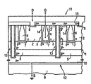
- Figure 1 shows an embodiment of the MOS-FETs according to the invention with the source connection on the back of the pane.
- a semiconductor body for example a silicon wafer, is n + -doped.
- the untreated semiconductor body 1 simultaneously forms the bulk zone 10.
- a p + -doped and a p - -doped layer are epitaxially applied to the front of the wafer 11 on the bulk zone 10. These layers are referred to below as inner zone 5.
- inner zone 5 Above the inner zone 5 are the drain zones 2 and source zones 3, which are also applied epitaxially.
- the drain zones 2 and the source zones 3 have the same doping, in the present case n-doping.
- the doping concentrations in the drain zones 2 and the source zones 3 should, but need not necessarily, be the same.
- the drain zones 2 and the source zones 3 are spaced apart from one another, where the distance between a drain zone 2 and a source zone 3 defines an intermediate cell zone 6.
- the intermediate cell zones 6 have the shape of vertical in the Semiconductor body 1 extending trenches. These trenches extend itself from the front face 11 of the semiconductor body 1 vertically over the drain zone 2 and the source zone 3 out into the inner zone 5 of the semiconductor body 1.
- the intermediate cell zones 6 should, but need not necessarily, extend into the inner zone 5. Rather, it is Freely selectable depth course.
- the intermediate cell zones 6 contain the gate electrodes 4.
- the gate electrodes 4 are connected to the gate terminal G.
- a gate material is because of its process engineering simple Manageability and its good conductivity prefer highly doped Polysilicon used.
- a gate oxide also titanium nitride or a metal silicide because of their good conductivity can be used.
- the gate electrodes 4 are through a gate oxide 14 from the adjacent drain zones 2 and source zones 3 and the inner zone 5 isolated.
- the gate electrodes 4 can be designed differently depending on the requirement his. In the present case, the gate electrodes 4 the shape of a tapering towards the top Bottle.
- the gate oxide 14 is preferably thermally grown Silicon dioxide used. Can be of particular advantage be the apex or reversal point of the Intermediate cell trenches 6 to be more U-shaped.
- the drain regions have embedded n + -doped regions and form the contact regions 8.
- the contact regions 8 are electrically contacted via a conventional metallization.
- the entirety of the drain contacts is short-circuited and forms the drain connection D.
- the drain contacts are isolated from the gate connections G by an intermediate oxide 15.
- the source zones 3 likewise have embedded n + -doped regions 3 '.
- vertical trenches 13 are etched into the source zones 3 '. These vertical trenches 13 contain conductive material that consists at least partially of doped polysilicon, titanium nitride, or metal. The vertical trenches 13 form a short circuit between the n + -doped source regions 3 ′ and the bulk zone 10.
- the bulk zone 10 has a large area on the rear side 12 of the pane contacted via a conventional metallization. This metallization forms the source connection S.
- p + -doped regions 7 are introduced directly under the intermediate cell zones 6 in the inner zone 5. These areas are referred to below as channel zones 7.
- the underlying technology step is commonly referred to as channel doping.
- the threshold voltage for the MOS-FETs can be precisely determined by introducing an exactly determinable doping concentration.
- the etched intermediate cell zones 6, in which the gate electrode 4 and the gate oxide 14 have not yet been introduced can advantageously be used as an implantation mask. It is also conceivable that the channel zone 7 is formed by a thin, p + -doped epitaxial layer between the inner zone 5 and drain / source zones 2, 3.
- the current flows from the source connection S on the rear side of the pane 12 via the bulk zone 10 and the vertical trenches 13 to the n + -doped source regions 3 '. From there, the current flows via the channel formed under the intermediate cell zones 6 to the drain region 2 and thus to the drain connection D.
- the source connection S is without Insulating layer attached to a heat sink or device housing 9.
- the ground potential of the source zone is therefore the same the potential of the device mass.
- heat sink 9 is preferred a copper block used. Due to the very high thermal conductivity This makes copper quick heat dissipation guaranteed by the semiconductor body 1.
- the MOS-FETs shown in Figure 1 are called normally-off called n-channel MOS-FETs.
- the line types from Drain / source zone 2, 3 and channel zone 7 are different.
- the MOS-FETs according to the invention also realize as self-conducting transistors.
- the conduction type of channel zone 7 is the same as the conduction type of Drain / source zones 2, 3.
- channel zone 7 must have drain and source zones 2, 3 touch.
- p-channel MOSFETs can also be used accordingly realize.
- the p + and p - -doped layers of the inner zone 5 and the drain / source zones 2, 3 are epitaxially applied to the semiconductor body 1, which simultaneously forms the bulk zone 10.
- the pane front side 11 is structured and the contact regions 8 of the drain zones 2 and the highly doped source regions 3 'are introduced by ion implantation.
- the front side of the pane 11 is structured again and the intermediate cell zones 6 are etched anisotropically.
- the p + -doped regions 7 are introduced into the inner zone 5 by ion implantation.
- a thin thermal silicon dioxide layer is then applied as gate oxide 14 in the intermediate cell zones 6.
- the intermediate cell zones 6 are filled with doped polysilicon as the material for the gate electrodes 4.
- Excess polysilicon is etched out of the intermediate cell zones 6 and the intermediate cell zones 6 are filled up with silicon dioxide.
- the front of the pane 11 is structured again and the trenches 13 are anisotropically etched to the depth of the bulk zone 10. A thin oxide is applied to the walls of the further trenches 13 and the trenches 13 are doped with titanium nitride or. Padded polysilicon.
- the source connection S on the rear side of the pane 12 is metallized over a large area.
- the pane front side 11 is structured and the drain connections D and gate connections G are metallized on the corresponding contacts and insulated from one another by an intermediate oxide 15.
- the source connection S is fastened to a heat sink 9 via a conductive solder.
Landscapes
- Electrodes Of Semiconductors (AREA)
- Insulated Gate Type Field-Effect Transistor (AREA)
- Metal-Oxide And Bipolar Metal-Oxide Semiconductor Integrated Circuits (AREA)
Claims (11)
- Dispositif à semi-conducteur contrôlable par effet de champ et intégré dans un corps semi-conducteur (1) en forme de disque, comportant une face avant (11) et une face arrière (12) de disque,avec au moins une zone de drain (2, 8) appartenant au premier type de conducteur ;avec au moins une zone de source (3, 3'), appartenant au premier type de conducteur, au voisinage de la face avant du disque (11) ;avec au moins une électrode de grille (4), isolée vis-à-vis de l'ensemble du corps semi-conducteur (1) par un oxyde de grille (14), alors qu'un raccordement de drain (D) et un raccordement de grille (G) se trouvent sur la face avant du disque (11) ;avec une zone de charge (10) appartenant au premier type de conducteur et qui est en contact, dans la zone de la face arrière du disque (12), avec un raccordement de source (S) ;avec des tranchées verticales (13) remplies de matériau conducteur et qui court-circuitent les zones de source (3, 3') en place sur la face avant (11) du disque, ainsi que la zone de charge (10) du corps semi-conducteur (1).
- Dispositif à semi-conducteur contrôlable par effet de champ selon la revendication 1,
caractérisé en ce que
le raccordement de source (S) est fixé sur un dissipateur thermique (9). - Dispositif à semi-conducteur contrôlable par effet de champ selon la revendication 2,
caractérisé en ce que
le dissipateur thermique (9) est un bloc de cuivre. - Dispositif à semi-conducteur contrôlable par effet de champ selon l'une des revendications 1-3,
caractérisé en ce que
la zone de charge (10) du corps semi-conducteur (1) présente une concentration de dopage très élevée. - Dispositif à semi-conducteur contrôlable par effet de champ selon la revendication 1,
caractérisé en ce que
le matériau conducteur des tranchées (13) contient du nitrure de titane ou du polysilicium dopé ou encore du métal. - Dispositif à semi-conducteur contrôlable par effet de champ selon l'une des revendications 4-5,
caractérisé en ce que
la zone de charge (10) présente une concentration de dopage supérieure à 1018 cm-3. - Dispositif à semi-conducteur contrôlable par effet de champ selon l'une des revendications 1-6,
caractérisé en ce que
il est prévu de mettre en place des zones de cellules intermédiaires (6) qui créent une distance entre les zones de drain (2, 8) et les zones de source (3, 3') et dans lesquelles sont placés à chaque fois une électrode de grille (4) et l'oxyde de grille (14). - Dispositif à semi-conducteur contrôlable par effet de champ selon la revendication 7,
caractérisé en ce que
l'on a mis en place directement en dessous des zones de cellules intermédiaires (6), de préférence par implantation d'ions, à chaque fois une zone de canal (7) appartenant au premier ou au second type de conducteur. - Dispositif à semi-conducteur contrôlable par effet de champ selon l'une des revendications 1-8,
caractérisé en ce que
dans les zones de drain (2), on a prévu, des régions de contact (8) qui présentent une très haute concentration de dopage et qui ont été mises en place dans le corps semi-conducteur (1) de préférence par implantation d'ions. - Dispositif à semi-conducteur contrôlable par effet de champ selon l'une des revendications 1-9,
caractérisé en ce que
le matériau des électrodes de grilles (4) est du polysilicium hautement dopé. - Procédé de fabrication d'un dispositifs à semi-conducteur contrôlable par effet de champ selon l'une des revendications 1-10, qui consiste à effectuer les opérations suivantes :on met au point un corps semi-conducteur en forme de disque, présentant une face avant (11) et une face arrière (12) de disque ;dans la zone de charge d'un corps semi-conducteur (1), on sépare les diverses couches épitaxiales de la zone intérieure (5) ;dans la zone intérieure (5), on sépare par épitaxie la zone de drain 2 et de source 3 ;on structure la face avant (11) du disque et l'on met en place, par l'implantation d'ions, la région de contact (8) et les zones de source hautement dopées (3');on structure à nouveau la face avant (11) du disque et l'on décape les zones de cellules intermédiaires (6) de manière anisotrope ;en utilisant le masque de décapage, on met en place les zones de canal (7) par implantation d'ions ;en utilisant le masque de décapage, on met en place par voie thermique une couche mince de dioxyde de silicium, en tant qu'oxyde de grille (14), sur les parois de tranchée des zones de cellules intermédiaires (6) ; on remplit celles-ci de polysilicium comme matériau de grille, on enlève par décapage le polysilicium en excédent se trouvant dans les zones de cellules intermédiaires (6) et on achève de remplir les cellules (6) avec du dioxyde de silicium comme matériau de grille ;on structure à nouveau la face avant (11) du disque et l'on met en place par décapage de manière anisotrope, au voisinage des zones de source (3, 3'), les tranchées (13) jusque dans la profondeur de la zone de charge (3) ;on métallise sur une grande surface, sur la face arrière (12) du disque, le raccordement de source (S) ;on métallise le raccordement de drain (D) et le raccordement de grille (G) sur la face avant du disque (11) auprès des contacts correspondants et on les isole l'un vis-à-vis de l'autre par un oxyde intermédiaire (15) ;on fixe le raccordement de source (S) de manière conductrice sur le dissipateur thermique (9).
Applications Claiming Priority (2)
| Application Number | Priority Date | Filing Date | Title |
|---|---|---|---|
| DE19638438A DE19638438A1 (de) | 1996-09-19 | 1996-09-19 | Durch Feldeffekt steuerbares, vertikales Halbleiterbauelement |
| DE19638438 | 1996-09-19 |
Publications (2)
| Publication Number | Publication Date |
|---|---|
| EP0833386A1 EP0833386A1 (fr) | 1998-04-01 |
| EP0833386B1 true EP0833386B1 (fr) | 2004-02-04 |
Family
ID=7806244
Family Applications (1)
| Application Number | Title | Priority Date | Filing Date |
|---|---|---|---|
| EP97113580A Expired - Lifetime EP0833386B1 (fr) | 1996-09-19 | 1997-08-05 | Dispositif semiconducteur vertical contrôlable par effet de champ |
Country Status (5)
| Country | Link |
|---|---|
| US (2) | US5945708A (fr) |
| EP (1) | EP0833386B1 (fr) |
| JP (1) | JP3728073B2 (fr) |
| KR (1) | KR100446583B1 (fr) |
| DE (2) | DE19638438A1 (fr) |
Families Citing this family (45)
| Publication number | Priority date | Publication date | Assignee | Title |
|---|---|---|---|---|
| AU705177B1 (en) * | 1997-11-26 | 1999-05-20 | Kabushiki Kaisha Toshiba | Semiconductor device |
| US6124612A (en) * | 1998-01-15 | 2000-09-26 | Siemens Aktiengesellschaft | FET with source-substrate connection and method for producing the FET |
| US6118147A (en) * | 1998-07-07 | 2000-09-12 | Advanced Micro Devices, Inc. | Double density non-volatile memory cells |
| DE19923522A1 (de) * | 1999-05-21 | 2000-11-30 | Siemens Ag | Source-Down-Leistungstransistor |
| DE10004984A1 (de) * | 2000-02-04 | 2001-08-16 | Infineon Technologies Ag | Vertikales Halbleiterbauelement mit Source-Down-Design und entsprechendes Herstellungsverfahren |
| US6586833B2 (en) * | 2000-11-16 | 2003-07-01 | Silicon Semiconductor Corporation | Packaged power devices having vertical power mosfets therein that are flip-chip mounted to slotted gate electrode strip lines |
| DE10061529A1 (de) * | 2000-12-11 | 2002-06-27 | Infineon Technologies Ag | Feldeffekt gesteuertes Halbleiterbauelement und Verfahren |
| US7132712B2 (en) | 2002-11-05 | 2006-11-07 | Fairchild Semiconductor Corporation | Trench structure having one or more diodes embedded therein adjacent a PN junction |
| JP4171268B2 (ja) * | 2001-09-25 | 2008-10-22 | 三洋電機株式会社 | 半導体装置およびその製造方法 |
| US7061066B2 (en) | 2001-10-17 | 2006-06-13 | Fairchild Semiconductor Corporation | Schottky diode using charge balance structure |
| US6795337B2 (en) * | 2002-06-28 | 2004-09-21 | Progressant Technologies, Inc. | Negative differential resistance (NDR) elements and memory device using the same |
| KR100593445B1 (ko) * | 2004-02-13 | 2006-06-28 | 삼성전자주식회사 | 채널부 홀들 사이에 채널 영역을 갖는 트랜지스터들 및 그제조방법들 |
| US7352036B2 (en) | 2004-08-03 | 2008-04-01 | Fairchild Semiconductor Corporation | Semiconductor power device having a top-side drain using a sinker trench |
| CN100416854C (zh) * | 2004-09-02 | 2008-09-03 | 国际整流器公司 | 顶部漏极型金属氧化物半导体栅控器件 |
| DE102004045966B4 (de) * | 2004-09-22 | 2006-08-31 | Infineon Technologies Austria Ag | Vertikal-Feldeffekttransistor in Source-Down-Struktur |
| DE102005013533B4 (de) * | 2005-03-23 | 2010-04-29 | Infineon Technologies Austria Ag | Halbbrücken-/Vollbrücken-Schaltungsanordnung sowie dafür geeigneter p-Kanal-MOS-Feldeffekttransistor |
| AT504998A2 (de) | 2005-04-06 | 2008-09-15 | Fairchild Semiconductor | Trenched-gate-feldeffekttransistoren und verfahren zum bilden derselben |
| JP2006324488A (ja) * | 2005-05-19 | 2006-11-30 | Nec Electronics Corp | 半導体装置及びその製造方法 |
| JP2007184553A (ja) | 2005-12-06 | 2007-07-19 | Sanyo Electric Co Ltd | 半導体装置及びその製造方法 |
| US7446374B2 (en) | 2006-03-24 | 2008-11-04 | Fairchild Semiconductor Corporation | High density trench FET with integrated Schottky diode and method of manufacture |
| US7319256B1 (en) | 2006-06-19 | 2008-01-15 | Fairchild Semiconductor Corporation | Shielded gate trench FET with the shield and gate electrodes being connected together |
| US7960781B2 (en) * | 2008-09-08 | 2011-06-14 | Semiconductor Components Industries, Llc | Semiconductor device having vertical charge-compensated structure and sub-surface connecting layer and method |
| US10205017B2 (en) * | 2009-06-17 | 2019-02-12 | Alpha And Omega Semiconductor Incorporated | Bottom source NMOS triggered Zener clamp for configuring an ultra-low voltage transient voltage suppressor (TVS) |
| US8372714B2 (en) * | 2010-06-28 | 2013-02-12 | Macronix International Co., Ltd. | Semiconductor device and method of manufacturing a semiconductor device |
| TWI396230B (zh) * | 2010-06-30 | 2013-05-11 | Macronix Int Co Ltd | 半導體裝置及其製造方法 |
| US8519473B2 (en) | 2010-07-14 | 2013-08-27 | Infineon Technologies Ag | Vertical transistor component |
| US8373449B2 (en) | 2010-12-30 | 2013-02-12 | Infineon Technologies Ag | Circuit arrangement including a common source sense-FET |
| US20120168819A1 (en) * | 2011-01-03 | 2012-07-05 | Fabio Alessio Marino | Semiconductor pillar power MOS |
| US8487371B2 (en) | 2011-03-29 | 2013-07-16 | Fairchild Semiconductor Corporation | Vertical MOSFET transistor having source/drain contacts disposed on the same side and method for manufacturing the same |
| US8471331B2 (en) | 2011-08-15 | 2013-06-25 | Semiconductor Components Industries, Llc | Method of making an insulated gate semiconductor device with source-substrate connection and structure |
| US8816503B2 (en) * | 2011-08-29 | 2014-08-26 | Infineon Technologies Austria Ag | Semiconductor device with buried electrode |
| US10032878B2 (en) | 2011-09-23 | 2018-07-24 | Infineon Technologies Ag | Semiconductor device with a semiconductor via and laterally connected electrode |
| US9324829B2 (en) | 2011-09-23 | 2016-04-26 | Infineon Technologies Ag | Method of forming a trench electrode device with wider and narrower regions |
| CN103137655B (zh) * | 2011-11-29 | 2016-04-20 | 万国半导体股份有限公司 | 具有底部源极的功率mosfet器件及其制作方法 |
| JP2013131512A (ja) * | 2011-12-20 | 2013-07-04 | Sumitomo Electric Ind Ltd | 半導体装置およびその製造方法 |
| JP2013145770A (ja) | 2012-01-13 | 2013-07-25 | Sumitomo Electric Ind Ltd | 半導体装置およびその製造方法 |
| US8546875B1 (en) * | 2012-03-14 | 2013-10-01 | Infineon Technologies Austria Ag | Vertical transistor having edge termination structure |
| US9123559B2 (en) | 2013-05-31 | 2015-09-01 | Infineon Technologies Ag | Method for producing a semiconductor component |
| US9559198B2 (en) | 2013-08-27 | 2017-01-31 | Nxp Usa, Inc. | Semiconductor device and method of manufacture therefor |
| US9837526B2 (en) | 2014-12-08 | 2017-12-05 | Nxp Usa, Inc. | Semiconductor device wtih an interconnecting semiconductor electrode between first and second semiconductor electrodes and method of manufacture therefor |
| US9443845B1 (en) | 2015-02-23 | 2016-09-13 | Freescale Semiconductor, Inc. | Transistor body control circuit and an integrated circuit |
| US9472662B2 (en) * | 2015-02-23 | 2016-10-18 | Freescale Semiconductor, Inc. | Bidirectional power transistor with shallow body trench |
| US10348295B2 (en) | 2015-11-19 | 2019-07-09 | Nxp Usa, Inc. | Packaged unidirectional power transistor and control circuit therefore |
| TWI601295B (zh) * | 2016-08-25 | 2017-10-01 | 綠星電子股份有限公司 | 斷閘極金氧半場效電晶體 |
| US11404370B2 (en) * | 2019-11-27 | 2022-08-02 | Infineon Technologies Ag | Failure structure in semiconductor device |
Family Cites Families (11)
| Publication number | Priority date | Publication date | Assignee | Title |
|---|---|---|---|---|
| NL157456B (nl) * | 1968-07-30 | 1978-07-17 | Philips Nv | Halfgeleiderinrichting in een isolerende kunststofomhulling. |
| US4446476A (en) * | 1981-06-30 | 1984-05-01 | International Business Machines Corporation | Integrated circuit having a sublayer electrical contact and fabrication thereof |
| JPS6252969A (ja) * | 1985-08-30 | 1987-03-07 | Nippon Texas Instr Kk | 絶縁ゲ−ト型電界効果半導体装置 |
| US4791462A (en) * | 1987-09-10 | 1988-12-13 | Siliconix Incorporated | Dense vertical j-MOS transistor |
| US4835586A (en) * | 1987-09-21 | 1989-05-30 | Siliconix Incorporated | Dual-gate high density fet |
| JPH0294477A (ja) * | 1988-09-30 | 1990-04-05 | Toshiba Corp | 半導体装置及びその製造方法 |
| US5023196A (en) * | 1990-01-29 | 1991-06-11 | Motorola Inc. | Method for forming a MOSFET with substrate source contact |
| US5539238A (en) * | 1992-09-02 | 1996-07-23 | Texas Instruments Incorporated | Area efficient high voltage Mosfets with vertical resurf drift regions |
| JPH07249770A (ja) * | 1994-03-10 | 1995-09-26 | Toshiba Corp | 半導体装置及びその製造方法 |
| US5488236A (en) * | 1994-05-26 | 1996-01-30 | North Carolina State University | Latch-up resistant bipolar transistor with trench IGFET and buried collector |
| JP3325736B2 (ja) * | 1995-02-09 | 2002-09-17 | 三菱電機株式会社 | 絶縁ゲート型半導体装置 |
-
1996
- 1996-09-19 DE DE19638438A patent/DE19638438A1/de not_active Withdrawn
-
1997
- 1997-08-05 EP EP97113580A patent/EP0833386B1/fr not_active Expired - Lifetime
- 1997-08-05 DE DE59711273T patent/DE59711273D1/de not_active Expired - Lifetime
- 1997-09-10 KR KR1019970046462A patent/KR100446583B1/ko not_active Expired - Fee Related
- 1997-09-17 JP JP27043597A patent/JP3728073B2/ja not_active Expired - Lifetime
- 1997-09-19 US US08/933,537 patent/US5945708A/en not_active Expired - Lifetime
-
1999
- 1999-05-19 US US09/314,192 patent/US6284604B1/en not_active Expired - Lifetime
Also Published As
| Publication number | Publication date |
|---|---|
| JP3728073B2 (ja) | 2005-12-21 |
| US5945708A (en) | 1999-08-31 |
| DE59711273D1 (de) | 2004-03-11 |
| EP0833386A1 (fr) | 1998-04-01 |
| KR100446583B1 (ko) | 2004-10-14 |
| KR19980024482A (ko) | 1998-07-06 |
| DE19638438A1 (de) | 1998-04-02 |
| US6284604B1 (en) | 2001-09-04 |
| JPH10107285A (ja) | 1998-04-24 |
Similar Documents
| Publication | Publication Date | Title |
|---|---|---|
| EP0833386B1 (fr) | Dispositif semiconducteur vertical contrôlable par effet de champ | |
| DE19638439C2 (de) | Durch Feldeffekt steuerbares, vertikales Halbleiterbauelement und Herstellungsverfahren | |
| DE19539541B4 (de) | Lateraler Trench-MISFET und Verfahren zu seiner Herstellung | |
| DE112015004515B4 (de) | Halbleitervorrichtungen | |
| DE69621200T2 (de) | Durchgriff-feldeffekttransistor | |
| DE69616013T2 (de) | Halbleiteranordnung vom hochspannungs-ldmos-typ | |
| DE102016104256B3 (de) | Transistorzellen und Kompensationsstruktur aufweisende Halbleitervorrichtung mit breitem Bandabstand | |
| DE69316256T2 (de) | Hochspannungstruktur mit oxydisolierter Source und RESURF-Drift-Zone in Massivsilizium | |
| DE102016102493B3 (de) | Halbleitervorrichtung mit einem temperatursensor, temperatursensor und verfahren zum herstellen einer halbleitervorrichtung mit einem temperatursensor | |
| DE102016101676B3 (de) | Elektrische schaltung, die eine halbleitervorrichtung mit einem ersten transistor und einem zweiten transistor und eine steuerschaltung enthält | |
| DE102015108440B3 (de) | Streifenförmige elektrodenstruktur einschliesslich eines hauptteiles mit einer feldelektrode und eines die elektrodenstruktur abschliessenden endteiles | |
| WO2000042665A1 (fr) | Composant de puissance mos et procede de fabrication dudit composant | |
| EP0888639A1 (fr) | Composant a semi-conducteur commande par effet de champ | |
| DE3537004A1 (de) | Vdmos-baustein | |
| WO2000002250A1 (fr) | Composant semi-conducteur vertical a champ superficiel electrique reduit | |
| DE102016101679A1 (de) | Halbleitervorrichtung mit einem lateralen Transistor | |
| DE102015119771A1 (de) | Halbleitervorrichtung mit einem ersten Transistor und einem zweiten Transistor | |
| DE102009011349B4 (de) | Halbleiterbauelemente und Verfahren zur Herstellung von Halbleiterchips | |
| EP1245050B1 (fr) | Element de commutation a semi-conducteur commandable a blocage bidirectionnel | |
| DE4122712A1 (de) | Halbleitervorrichtung | |
| DE4104588A1 (de) | Halbleiterbauelement mit einem leitfaehigkeitsmodulations-misfet | |
| DE19638437C2 (de) | Durch Feldeffekt steuerbares Halbleiterbauelement und Verfahren zu dessen Herstellung | |
| EP0586716B1 (fr) | MOSFET de puissance à stabilité d'avalanche améliorée | |
| DE102023107534B4 (de) | Halbleitervorrichtung mit breiter bandlücke | |
| WO2000044031A2 (fr) | Ensemble transistor de puissance a grande resistance dielectrique |
Legal Events
| Date | Code | Title | Description |
|---|---|---|---|
| PUAI | Public reference made under article 153(3) epc to a published international application that has entered the european phase |
Free format text: ORIGINAL CODE: 0009012 |
|
| AK | Designated contracting states |
Kind code of ref document: A1 Designated state(s): DE FR GB IE IT |
|
| AX | Request for extension of the european patent |
Free format text: AL;LT;LV;RO;SI |
|
| 17P | Request for examination filed |
Effective date: 19980903 |
|
| AKX | Designation fees paid |
Free format text: DE FR GB IE IT |
|
| RBV | Designated contracting states (corrected) |
Designated state(s): DE FR GB IE IT |
|
| RAP1 | Party data changed (applicant data changed or rights of an application transferred) |
Owner name: INFINEON TECHNOLOGIES AG |
|
| 17Q | First examination report despatched |
Effective date: 20020703 |
|
| GRAP | Despatch of communication of intention to grant a patent |
Free format text: ORIGINAL CODE: EPIDOSNIGR1 |
|
| GRAS | Grant fee paid |
Free format text: ORIGINAL CODE: EPIDOSNIGR3 |
|
| GRAA | (expected) grant |
Free format text: ORIGINAL CODE: 0009210 |
|
| AK | Designated contracting states |
Kind code of ref document: B1 Designated state(s): DE FR GB IE IT |
|
| PG25 | Lapsed in a contracting state [announced via postgrant information from national office to epo] |
Ref country code: IE Free format text: LAPSE BECAUSE OF FAILURE TO SUBMIT A TRANSLATION OF THE DESCRIPTION OR TO PAY THE FEE WITHIN THE PRESCRIBED TIME-LIMIT Effective date: 20040204 Ref country code: GB Free format text: LAPSE BECAUSE OF FAILURE TO SUBMIT A TRANSLATION OF THE DESCRIPTION OR TO PAY THE FEE WITHIN THE PRESCRIBED TIME-LIMIT Effective date: 20040204 |
|
| REG | Reference to a national code |
Ref country code: GB Ref legal event code: FG4D Free format text: NOT ENGLISH |
|
| REG | Reference to a national code |
Ref country code: IE Ref legal event code: FG4D Free format text: GERMAN |
|
| REF | Corresponds to: |
Ref document number: 59711273 Country of ref document: DE Date of ref document: 20040311 Kind code of ref document: P |
|
| GBV | Gb: ep patent (uk) treated as always having been void in accordance with gb section 77(7)/1977 [no translation filed] |
Effective date: 20040204 |
|
| REG | Reference to a national code |
Ref country code: IE Ref legal event code: FD4D |
|
| ET | Fr: translation filed | ||
| PLBE | No opposition filed within time limit |
Free format text: ORIGINAL CODE: 0009261 |
|
| 26N | No opposition filed |
Effective date: 20041105 |
|
| PGFP | Annual fee paid to national office [announced via postgrant information from national office to epo] |
Ref country code: DE Payment date: 20151020 Year of fee payment: 19 |
|
| REG | Reference to a national code |
Ref country code: FR Ref legal event code: PLFP Year of fee payment: 20 |
|
| PGFP | Annual fee paid to national office [announced via postgrant information from national office to epo] |
Ref country code: IT Payment date: 20160825 Year of fee payment: 20 |
|
| PGFP | Annual fee paid to national office [announced via postgrant information from national office to epo] |
Ref country code: FR Payment date: 20160822 Year of fee payment: 20 |
|
| REG | Reference to a national code |
Ref country code: DE Ref legal event code: R119 Ref document number: 59711273 Country of ref document: DE |
|
| PG25 | Lapsed in a contracting state [announced via postgrant information from national office to epo] |
Ref country code: DE Free format text: LAPSE BECAUSE OF NON-PAYMENT OF DUE FEES Effective date: 20170301 |