EP0833477A2 - Verfahren zum Bestimmen einer Abtastphase - Google Patents
Verfahren zum Bestimmen einer Abtastphase Download PDFInfo
- Publication number
- EP0833477A2 EP0833477A2 EP97116088A EP97116088A EP0833477A2 EP 0833477 A2 EP0833477 A2 EP 0833477A2 EP 97116088 A EP97116088 A EP 97116088A EP 97116088 A EP97116088 A EP 97116088A EP 0833477 A2 EP0833477 A2 EP 0833477A2
- Authority
- EP
- European Patent Office
- Prior art keywords
- bit
- sampling phase
- data
- binary values
- aph
- Prior art date
- Legal status (The legal status is an assumption and is not a legal conclusion. Google has not performed a legal analysis and makes no representation as to the accuracy of the status listed.)
- Withdrawn
Links
Images
Classifications
-
- H—ELECTRICITY
- H04—ELECTRIC COMMUNICATION TECHNIQUE
- H04L—TRANSMISSION OF DIGITAL INFORMATION, e.g. TELEGRAPHIC COMMUNICATION
- H04L7/00—Arrangements for synchronising receiver with transmitter
- H04L7/04—Speed or phase control by synchronisation signals
- H04L7/041—Speed or phase control by synchronisation signals using special codes as synchronising signal
- H04L7/042—Detectors therefor, e.g. correlators, state machines
-
- H—ELECTRICITY
- H04—ELECTRIC COMMUNICATION TECHNIQUE
- H04L—TRANSMISSION OF DIGITAL INFORMATION, e.g. TELEGRAPHIC COMMUNICATION
- H04L7/00—Arrangements for synchronising receiver with transmitter
- H04L7/04—Speed or phase control by synchronisation signals
- H04L7/041—Speed or phase control by synchronisation signals using special codes as synchronising signal
- H04L7/046—Speed or phase control by synchronisation signals using special codes as synchronising signal using a dotting sequence
-
- H—ELECTRICITY
- H04—ELECTRIC COMMUNICATION TECHNIQUE
- H04L—TRANSMISSION OF DIGITAL INFORMATION, e.g. TELEGRAPHIC COMMUNICATION
- H04L7/00—Arrangements for synchronising receiver with transmitter
- H04L7/04—Speed or phase control by synchronisation signals
- H04L7/041—Speed or phase control by synchronisation signals using special codes as synchronising signal
- H04L7/044—Speed or phase control by synchronisation signals using special codes as synchronising signal using a single bit, e.g. start stop bit
Definitions
- the invention relates to a method for determining a sampling phase, by means of digital data from a digital Data stream can be obtained.
- the invention further relates to a device for performing the method.
- Such a method is e.g. for cordless telecommunication devices for wire-free transmission of data and Voice information used.
- cordless telecommunications in the home area there is often a transmission after DECT standard (Digital Enhanced Cordless Telecommunication) used.
- DECT standard Digital Enhanced Cordless Telecommunication
- TDMA Time Division Multiple Access is a time division multiplex frame of 10 ms.
- Such a time division frame is shown in Figure 1.
- 24 time channels are defined (channels 0 to 23 in FIG. 1), which provides a framework.
- This framework scheme is used so that for each frequency band twelve mobile end stations, so-called mobile stations MS, with a base station BS can work in duplex mode at the same time, i.e. Transfers are possible from the stations MS to BS and from BS to MS or from BS to MS and from MS to BS.
- the 24th Time channels are assigned a time slot of 417 ⁇ s each, within which the data is transmitted.
- a time frame also called "burst"
- burst 365 ⁇ s transmitted
- a data throughput 42 kbit / s.
- GS Guard Space GS
- time-division multiplex frame corresponds to a PH channel, the so-called "physical channel", which is based on the layer model for data transfers of the physical layer (physical layer) is assigned.
- the transmitted data packet of 420 bits is called a PH packet and contains a D field.
- H-L bit values corresponds to (H (High) - high level value; L (Low) - low level value) become 32 bits for synchronization and 388 bit for the transmission of user data NI (Net Information) used.
- NI Network Information
- a synchronization introductory word SY-EW which is also called the preamble.
- SY-EW becomes the synchronization initiated.
- this synchronization initiation word exists after base station BS Ideally, SY-EW from an L-H-L-H bit sequence corresponding to a 0101 bit sequence.
- the synchronization introduction word SY-EW from a periodic H-L-H-L bit sequence or a 1010 bit sequence.
- the bit sequence with the second 16 H-L bit values, the second Data bit sequence is a synchronization confirmation word SY-BW, with those with the synchronization introductory word SY-EW initiated synchronization must be confirmed. For such confirmation must be the synchronization confirmation word SY-BW at least for the most part of the data bits be recognized. Only then are those following the sync field Data accepted. The synchronization is then initiated, if it is assumed with a certain probability may have the sync initiation word SY-EW an L-H-L-H bit sequence or an H-L-H-L bit sequence.
- a communication system includes in the simplest form a base station and at least one mobile station. More complex systems, e.g. networked systems several base stations, each with several mobile stations. Due to the 24 time channels defined in the DECT standard can be assigned up to twelve mobile stations to each base station with the respective base station in duplex mode communicate. For the one defined in the DECT standard Time multiplex frame of 10 ms has the consequence that in Duplex operation every 5 ms of data from the base station to one Mobile station or vice versa.
- Figure 3 shows one for communication systems according to the DECT standard typical communication arrangement KA with non-wired Data transmission, the mobile station MS as Transmitting device SG and the base station BS as receiving device EG serves.
- the communication arrangement KA can also do this be modified that the base station BS as a transmitter SG and the mobile station MS serves as a receiving device EG.
- the transmitter SG has a transmitting antenna SA, through which one of the Transmitting device SG generates radio signal FS to receiving device EG is sent.
- the receiving device EG also has a receiving antenna EA.
- the communication system works according to the DECT standard with a high frequency carrier signal with a carrier frequency between 1.8 and 1.9 GHz, which with a in the Transmitter SG present digital broadcast data stream SDS modulated a transmitter-specific clock (also called phase) becomes.
- the digital present in the transmitter SG Data stream contains the necessary for wireless transmission Information.
- This information also includes the synchronization and user information already mentioned, which are contained in the PH packet of 420 bit data length are.
- this PH data packet is now in the sending device SG generates the modulated radio signal FS (carrier signal) and according to the DECT standard for data transmission in regular, time intervals specified by the time division multiplex frame ZMR for a period of time predetermined by the time slot transfer.
- Voice information to be able to decrypt the radio signal FS, i.e. the modulated carrier signal, in the receiving device EG can be demodulated.
- a digital receive data stream EDS which at a interference-free transmission of the radio signal FS the same bit pattern has, like the transmission data stream SDS.
- This trouble-free Receive data stream EDS is shown in block EG on the right.
- Bit pattern which is shown on the left in block EG.
- DE 42 36 775 C2 describes a method for determining the Known sampling phase, using the digital data from a digital data stream can be obtained.
- the incoming data are oversampled 9 times per digital value, so that for each Digital value a bit group with nine bit positions is generated.
- the optimal sampling phase i.e. the sampling time in the middle of a digital value
- the bit string at the beginning of each time frame (burst) i.e. the Preamble, evaluated.
- burst i.e. the Preamble
- Based on the known bit pattern determines the middle of a digital value and the associated one Sampling phase set for the rest of the time frame is held.
- This sampling phase becomes a clock signal constant frequency generated, with the help of the received data are scanned with bit accuracy and the received data stream is won.
- the 9-fold oversampled Receive data loaded into a register bank.
- the binary values in this register bank are compared with a predetermined pattern and the respective bit center is determined.
- the last digital value determined sampling phase leading to a Bit center heard, recorded and then for the rest of the time frame maintained.
- the ones previously identified within the bit pattern Bit centers and the associated sampling phases are not considered. So it's the bit center of one Digital values or data bits responsible for the determination the sampling phase and thus for the generation of the digital Data from the received digital data stream. If so This data bit is disturbed, you get from the known one Process an inaccurate sampling phase, resulting in increased bit error rates leads within the timeframe concerned.
- a scanning method and a Specify the scanning device which consists of a digital Data stream determined sampling phase with high accuracy in with respect to the center of the incoming data bits.
- a predetermined bit pattern containing digital data stream with a fixed Data rate becomes n times per digital value according to oversampling scanned;
- the sub-data bit sequence created during the scan becomes temporary in a serial register bank stored, with each scan in agreement with a clock pulse a shift of the stored sub-data bits in the register bank by one bit position and the sub data bit generated during the scanning into the first bit position the register bank is written;
- those in the register bank Sub-data bits contained are in bit groups of n-bit positions divided; Binary values of at least one matching one Bit position within at least two bit groups are compared to each other in a match checked; depending on the result of the comparison, the sampling phase fixed.
- matching bit positions are at least two bit groups evaluated, the serial in the register bank are saved.
- the comparison with a given one Bit patterns as target patterns as in DE 42 36 775 C2 are omitted.
- the evaluation of at least two bit groups increases the statistical certainty for the determination of the sampling phase. The greater the number of bit groups evaluated, the greater will this statistical certainty.
- the evaluation of four bit groups and from five bit positions within each bit group to one compared to the prior art increased accuracy of the sampling phase leads. Since there are several digital values or data bits contribute to the sampling phase at a particular point in time fixed and then maintained for the rest of the time frame is the risk of freezing an unfavorable sampling phase significantly reduced.
- the sensitivity of the receiving device is accordingly by the inventive method clearly improved.
- a device to determine a sampling phase with the features of Claim 12 specified According to another aspect of the invention, a device to determine a sampling phase with the features of Claim 12 specified.
- the achievable with this facility Advantages are essentially the same as those adjust themselves when performing the above-mentioned procedure.
- FIG. 4 shows the structure of a by means of a block diagram cordless (line-bound) telecommunication device 1 as e.g. as a base station or mobile station in one, e.g. Cordless communication system defined according to the DECT standard is usable.
- the telecommunication device 1 has in addition to functional units not shown in detail Receiving part 10 for the reception of for information transmission modulated analog RF signals AS, a digital part 13 for evaluation and further processing of one from the respective RF signal AS demodulated digital data stream DS as well a peripheral part 18 for outputting or forwarding the using the RF signal AS and the digital data stream DS transmitted information.
- the receiving part 10 of the telecommunication device 1 is with the output terminal of an antenna 11 connected.
- a radio transmission link 2 can the RF signals emitted by a transmitter 3 AS are received.
- the signals from antenna 11 are one Receiving device 12 fed to a receiving circuit 120 and a demodulation circuit 121 contains.
- the receiving circuit 120 prepares that received by the antenna 11 modulated analog RF signal AS for demodulation in the Demodulation circuit 121 on.
- demodulating the RF signal AS arises at the output of demodulation circuit 121 the digital data stream DS.
- This data stream DS is with a data rate of 1.152 Mbit / s via a data line 4 a control device 14 of the digital part 13 transmitted.
- the demodulation circuit 121 is via a first control line 5 directly connected to the control device 14. Furthermore, the demodulation circuit 121 is via a second Control line 6 and a compensation circuit 19 in the receiving part 10 connected to the control device 14.
- the computer 16 contains a microprocessor 160 and one with this connected digital memory 161.
- the computer 16 is for all control and programming processes in the Telecommunication device 1 responsible. For example the control module 14 indirectly via the bus interface 15 programmed by the microprocessor arrangement 16.
- the computer 16 also controls an ADPCM and CODEC circuit 17, what interface functions between the control device 14 and the peripheral part 18 takes over.
- the circuit receives implementation of its interface function 17 also control signals from the control device 14.
- Das Peripheral part 18 contains devices that are different from the digital part 13 processed digital data stream DS after a D / A conversion e.g. converted into acoustic signals or the Data stream DS to an external analog communication network passes on.
- FIG. 5 shows the basic structure in a block diagram of the digital part 13 according to FIG. 4, in particular the structure of the parts necessary for the synchronization of the receiving part 10 received digital data stream DS are required.
- the control device 14 contains a sampling phase generator 140, the digital data stream used to generate the sampling phase APH DS is fed.
- the sampling phase generator 140 is with an oscillator 141, a registration device 142 and a detection circuit 143 connected to the noisy signals recognizes and signals this.
- the oscillator 141 generates a clock signal TSI whose clock frequency is 9 times the frequency with which the digital Data stream DS is transmitted.
- the clock signal TSI is excluded the sampling phase generator 140 also the registration device 142 fed.
- the registration device 142 also receives one from the computer 16 of the digital part 13 generated status message SM2 and a status message generated by the detection circuit 143 SM3. From the status messages SM0, SM2 and SM3 and the clock signal The registration facility generates the status message TSI SM1, which is fed to the sampling phase generator 140 becomes.
- the status messages SM0 to SM3 their function in context with the structure of the control device shown in Figure 6 14 still to be described are dynamic ones Time-changing status messages in the control device 14 arranged for the generation of the sampling phase APH Assemblies 140, 142, 143.
- the sampling phase generator When the last status message SM1 is received, the sampling phase generator generates 140 from the digital data stream DS and the clock signal TSI the final sampling phase APH, which then in addition to the digital data stream DS for the synchronization of a Synchronization arrangement 144 is supplied.
- the of the sampling phase generated by the sampling phase generator 140 however, not just the synchronization arrangement 144, but also supplied to the registration device 142.
- this registration device 142 Along with the data stream also supplied to the registration device 142 DS, this registration device 142 generates the control signal STS, which via the control line 5 of Figure 4 Demodulation circuit 121 and the control line 6 after 4 of the compensation circuit 19 of the receiving part 10 is fed.
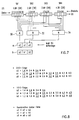
- FIG. 6 schematically shows the structure in a block diagram a device for sampling phase generation, the sampling phase generator 140, the oscillator 141, the registration device 142 and the detection circuit 143 contains (cf. Figure 5).
- the sampling phase generator 140 contains a suppression circuit 1400, a register bank 1401, an over a bus interface device 1402 with the register bank 1401 connected bit sequence detection circuit 1403 and one Selection circuit 1404.
- the sampling phase generator 140 serves to do this, together with the registration device 142 and the Detection circuit 143 from the digital data stream DS within a period of time by the sync word SY-EW (preamble) defined according to Figures 2 and 3 is, the sampling phase APH for synchronization in with respect to the data stream DS.
- the data stream DS first becomes the suppression circuit 1400 fed.
- This suppression circuit 1400 operates according to the shift register principle, i.e. to push the Data stream DS a clock signal must be applied.
- Fall becomes the clock signal generated by the oscillator 141 TSI with an n-fold clock frequency TFn on the suppression circuit Given 1400.
- the digital data stream DS is bit by bit with a sampling rate sampled according to the clock frequency TFn.
- Each one Data bit DB of the digital data stream DS is thus in one Series of sub-data bits SDB disassembled and then examined for errors. Multiple consecutive data bits DB result several series of sub data bits SDB; these series are in hereinafter referred to as sub data bit sequence SDBF.
- the suppression circuit 1400 for each data bit DB Data stream DS nine sub-data bits SDB generated as samples.
- the function of the suppressor circuit 1400 is to ascertained and e.g. inhomogeneous caused by noise H-L-H bitsubsequence or an L-H-L bitsubsequence of Recognize and suppress sub-data bit sequence SDBF.
- the suppression circuit 1400 downstream register bank 1401 only such data bits DB of the digital data stream DS are supplied at which a sub-data bit sequence SDBF without an inhomogeneous "H-L-H" bit sub-sequence or "L-H-L” bit sub-sequence is present.
- Each shift register SR1 to SR4 stores a data bit DB of the data stream DS. It follows that when scanning the Data bits DB a total of 36 sub data bits SDB as a sub data bit sequence SDBF are buffered in the register bank 1401. With each clock of the clock signal TSI changes in the Shift registers SR1 to SR4 cached sub-data bits SDS. After 36 consecutive clocks of the clock signal TSI is that in the zeroth bit position of the shift register SR1 cached sub data bit in the last bit position of the Shift register SR4 pushed through.
- the one in the register bank 1401 Sub-data bit sequence buffered at each clock time SDBF is via the bus interface device 1402 to the bit sequence detection circuit 1403, to the detection circuit 143 and to a bit equality detection circuit 1420 transferred to the registration device 142.
- the Bit sequence detection circuit 1403 has the task of 0101 or the 1010 bit sequence of the preamble of the data stream DS recognize and determine the point in time at which the respective Bit has reached its bit center. This middle bit sets then set the sampling time for the subsequent bits. in the The method used for this is explained in more detail below.
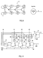
- FIG. 7 shows schematically how the binary values contained in the individual shift registers SR1 to SR4 are linked to one another.
- a first AND gate 30 the binary values of the fourth bit position of the bit groups stored in the shift registers SR1 to SR4 (1st bit to 4th bit) are linked together. It should be noted that the binary values of the different bit groups are negated alternately in order to be able to correctly evaluate the sequence of 1010 values or 0101 values.
- the fourth bit position in the respective shift register SR4 to SR1 is the middle bit position.
- the binary values of the third and fifth bit positions of the four shift registers SR1 to SR4 are linked, ie the bit positions adjacent to the middle bit position.
- the respective coefficients of the data words a and b are ORed further, so that the result is the data word c with the coefficients c2, c1 and c0, the data word c being c2 2 + c1 1 + c0 0 to base 2 is interpreted.
- the highest value of the data word c is thus in binary notation 111 and in decimal notation 7; its lowest value is 000 or decimal 0.
- Data words a, b and c represent a measure of the correspondence of the respective binary values in the shift registers SR1 to SR4.
- the counter Z is shown as a Moore automaton.
- the output signal A is a variable which indicates for how many cycles the value of the data word c has remained constant.
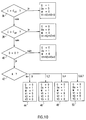
- the input signal G on the basis of which a new state s0 to s7 is established, is generated in accordance with the sequence steps according to FIG. 10.
- Figure 10 shows a flow chart, the processing of which already mentioned variable G is generated, which at the counter 9 is required as an input variable.
- Da and D which ones as an input signal and output signal for an edge triggered Flip-flop according to FIG. 11 are used; the size M, which acts as an input signal to the circuitry 11 is used and indicates that a maximum has been determined; also the binary sizes V1, V2 and V3, which are also in the circuit arrangement according to FIG 11 are used and a shift of one or several cycles cause, as in connection with FIG. 11 is explained.
- step 36 it is determined in the first step 36 whether the current value of the data word c matches the previous value of the data word c alt . If this is the case, the variable G is set to 1, the other variables D, M, V1 to V3 are set to 0. Setting the variable G to 1 causes the counter Z according to FIG. 9 to be counted up by 1, that is to say its output signal A is increased by 1. If no match has been found in step 36, then in subsequent step 38 it is checked whether the current value of the data word c is greater than the previous value c old . If this is the case, the variable G is set to 0, which means that the counter Z according to FIG. 9 is reset and assumes the state s0. The other sizes are set to 0.
- step 38 If a negative result is determined in step 38, ie the current value of the data word c is less than the previous value c alt - the maximum of the value was therefore undershot - then in the following step 40 the value of the variable D is checked. If the variable D has the value 1, the variable G is set to 0, the size Da to 1 and the other sizes to 0.
- test result in step 40 is positive, it is dependent on the different from the current meter reading according to FIG Sizes set.
- Figure 11 shows a circuit arrangement for generating a Recognition signal ESI, which by a predetermined number of clocks, which are defined by the variables V1, V2, V3 against a maximum pulse is shifted by the variable M is defined with value 1.
- the circuit arrangement contains four cascaded flip-flops 52 to 58 which can be controlled by the clock pulse TSI. Furthermore contains the circuit arrangement AND gates 60 to 70, an input AND gate 72 and OR gates 74 to 78.
- the link elements mentioned have inverting inputs that are in the Figure 11 are identified by a dot.
- a flip-flop 51 is shown at the top right of FIG. 11, which serves to delay the variable Da by one clock, i.e. the output variable D takes the after a clock pulse Value of the variable Da an.
- the mode of operation of the circuit arrangement according to FIG. 11 is as follows.
- the set in the sequence control according to Figure 10 Variables M, V1, V2, V3, Da and D are called rectangular pulses interpreted, depending on the switching logic used the value 0 of a variable is an L value and the value 1 is an H value or vice versa.
- the variables according to block 44 in Figure 10 are defined, i.e. for a payer A equal 0.
- the input AND gate 72 generates a logic 1 at its exit.
- the flip-flop 52 is in the next clock generate a logical 1 at its output, whereupon the AND gate 60 has a logic 1 at its output generated and via the OR gate 74, the input of the flip-flop 54 is set to logic 1.
- the next bar will be similar Way the input of flip-flop 56 is set to logic 1, and at the next but one clock, the input of the flip-flop 80.
- the following clock appears at the output of the flip-flop 58 a logical 1, i.e. the detection signal is ESI set to logical 1. It should therefore be noted that the Change of state from logic 0 to 1 of the detection signal ESI by four bars compared to the appearance of a logical 1 where the variable M is shifted. Since the variable indicates M that a maximum has been recognized is the detection signal ESI delayed by four cycles compared to this maximum detection.
- the Variables set according to block 46 In the event that the counter reading A is 1 or 2, i.e. the maximum was for two or three bars, the Variables set according to block 46.
- the variable has V1 accordingly a logical 1, with the result that the input AND gate 72 is blocked. Lie at the input of the AND gate 62 however the variables V1 and M each with logical 1, and the input of flip-flop 64 is set. After expiration of three clocks of the clock signal TSI appears at the output of the Flip-flops 58 as a detection signal ESI a logical 1.
- Das Detection signal ESI is therefore opposite to the setting of the variables M shifted to logical 1 by three measures.
- variable V2 there is a two shift Cycles when the variable V2 is set to logic 1, i.e. the variables are defined according to block 48 in FIG. 9, which is assigned to the meter reading A equal to 3 or 4.
- the variables defined according to block 50 At a counter reading A is 5, 6 or 7 are the variables defined according to block 50, i.e. the variable V3 has the Logical value 1.
- the Appear variable M As logical 1 and the output signal of the flip-flop 58, the detection signal ESI, by one Clock of the clock signal TSI.
- the selection circuit is used to correct the sampling phase APH 1404 used according to Figure 6. For example, it is as Counter formed by the oscillator 141 with clock pulses is controlled and each by the detection signal ESI reset to the bit center of the individual data bits becomes.
- the bit sequence detection circuit 1403 With the delivery of the detection signal ESI, the bit sequence detection circuit 1403 to a counter 1421 of the Registration device 142 from the status message SM0. With this Status message SM0 is communicated to the counter 1421, that the first 0101 or 1010 bit sequence has been recognized is.
- the counter 1421 which is also provided by the oscillator Is clocked, counts the number of transmitted to it Status messages SM0.
- the counter 1421 waits for an additional signal ZS from of bit equality detection circuit 1420 and evaluates the Status messages SM3, SM2 of the detection circuit 143 and the Microprocessor arrangement 16 from. Depending on the status messages SM2, SM3 or the additional signal ZS are the counting device 1421 the status message via an OR gate 1422 SM1 to the selection circuit 1404.
- the counter device 1421 With the status message SM3, the counter device 1421, in the event that a "noisy" actual data stream I-DS or Data stream DS was recognized, reset. With the status message SM2 is informed to counter 1421 whether that Sync actuation word SY-BW was recognized, i.e. a DECT-specific Time slot TS is present.
Landscapes
- Engineering & Computer Science (AREA)
- Computer Networks & Wireless Communication (AREA)
- Signal Processing (AREA)
- Synchronisation In Digital Transmission Systems (AREA)
- Time-Division Multiplex Systems (AREA)
- Stabilization Of Oscillater, Synchronisation, Frequency Synthesizers (AREA)
Abstract
Description
- Figur 1 bis 3
- Festlegungen der Datenübertragung gemäß dem DECT-Standard sowie die leitungsungebundene Datenübertragung zwischen einem Sendegerät und einem Empfangsgerät,
- Figur 4
- ein Blockschaltbild mit den wesentlichen Funktionseinheiten eines schnurlos arbeitenden Telekommunikationsgerätes mit einem Empfangsteil und einem Digitalteil,
- Figur 5
- ein Blockschaltbild mit wichtigen Funktionseinheiten des Digitalteils für die Demodulation eines modulierten Analogsignales und für die Erzeugung einer Abtastphase zur Synchronisation eines digitalen asynchronen Datenstroms auf ein gerätespezifisches Taktsignal,
- Figur 6
- ein Blockschaltbild der Einrichtung zum Erzeugen einer Abtastphase,
- Figur 7
- eine Schaltungsanordnung zum Erzeugen eines Datenwortes, anhand dessen ein Erkennungssignal und damit die Abtastphase festgelegt wird,
- Figur 8
- logische Verknüpfungen in Tabellenform zum Erzeugen des in Figur 7 dargestellten Datenwortes,
- Figur 9
- einen Zähler zur Ermittlung der Anzahl von Taktimpulsen bei denen der Wert des Datenwortes unverändert ist,
- Figur 10
- ein Flußdiagramm, welches Verfahrensschritte zur Erkennung des Maximum des Wertes des Datenwortes zeigt, und
- Figur 11
- eine Schaltungsanordnung zur Festlegung des Erkennungssignals und damit der Abtastphase auf der Grundlage der Anzahl der Taktimpulse für das Maximum.
Claims (19)
- Verfahren zum Bestimmen einer Abtastphase (APH), mittels der digitale Daten aus einem digitalen Datenstrom (DS) gewonnen werden, mit den folgenden Schritten:der ein vorbestimmtes Bitmuster enthaltende digitale Datenstrom (DS) mit einer festgelegten Datenrate wird je Digitalwert (DB) gemäß einer Überabtastung n-fach abgetastet,die bei der Abtastung entstehende Subdaten-Bitfolge (SDBF) wird in einer seriell arbeitenden Registerbank (1401) vorübergehend gespeichert, wobei je Abtastung in Übereinstimmung mit einem Taktimpuls (TSI) eine Verschiebung der gespeicherten Subdatenbits (SDB) in der Registerbank (1401) um eine Bitstelle erfolgt und das bei der Abtastung erzeugte Subdatenbit (SDB) in die erste Bitstelle der Registerbank (1401) geschrieben wird,die in der Registerbank (1401) enthaltenen Subdatenbits (SDB) werden in Bitgruppen (DB) von n-Bitstellen unterteilt,Binärwerte mindestens einer übereinstimmenden Bitstelle innerhalb mindestens zweier Bitgruppen (DB) werden miteinander in einem Vergleich auf Übereinstimmung überprüft,abhängig vom Ergebnis des Vergleichs wird die Abtastphase (APH) festgelegt.
- Verfahren nach Anspruch 1, dadurch gekennzeichnet, daß das Bitmuster eine L-H-L-H-Bitsequenz oder eine H-L-H-L-Bitsequenz ist.
- Verfahren nach Anspruch 1 oder 2, dadurch gekennzeichnet, daß bei der Überabtastung n=9 ist.
- Verfahren nach einem der vorhergehenden Ansprüche, dadurch gekennzeichnet, daß beim Vergleich der Binärwerte übereinstimmende Bitstellen von vier aufeinander folgenden Bitgruppen (DB) verwendet werden.
- Verfahren nach einem der vorhergehenden Ansprüche, dadurch gekennzeichnet, daß zum Vergleich die Binärwerte einer logischen UND-Verknüpfung unterzogen werden, wobei die Binärwerte aufeinander folgender Bitgruppen (DB) abwechseln negiert werden.
- Verfahren nach einem der vorhergehenden Ansprüche, dadurch gekennzeichnet, daß als übereinstimmende Bitstelle die mittlere Bitstelle (4. Bitstelle) einer jeden Bitgruppe (DB) verwendet wird.
- Verfahren nach Anspruch 6, dadurch gekennzeichnet, daß die Binärwerte der der mittleren Bitstelle benachbarten beiden Bitstellen (3. und 5. Bitstelle) der Bitgruppen (DB) einer zweiten UND-Verknüpfung unterzogen werden, und daß die Abtastphase (APH) abhängig vom Ergebnis der ersten UND-Verknüpfung und der zweiten UND-Verknüpfung festgelegt wird.
- Verfahren nach Anspruch 7, dadurch gekennzeichnet, daß die Binärwerte der an die benachbarten Bitstellen angrenzenden Bitstellen (2. und 6. Bitstelle) der Bitgruppen (DB) einer dritten UND-Verknüpfung unterzogen werden, und daß die Abtastphase (APH) abhängig vom Ergebnis der ersten UND-Verknüpfung, der zweiten UND-Verknüpfung und der dritten UND-Verknüpfung festgelegt wird.
- Verfahren nach einem der vorhergehenden Ansprüche, dadurch gekennzeichnet, daß die Zahl übereinstimmender nicht negierter Binärwerte und negierter Binärwerte je Taktimpuls (TSI) festgestellt wird, daß die Anzahl der Taktimpulse (TSI) ermittelt wird, für die die Zahl gleich bleibt, und daß die Abtastphase (APH) abhängig von dieser Anzahl festgelegt wird.
- Verfahren nach Anspruch 9, dadurch gekennzeichnet, daß die Abtastphase (APH) so festgelegt ist, daß sie im wesentlichen mit dem Taktimpuls übereinstimmt, der durch die halbe Anzahl definiert ist.
- Verfahren nach einem der vorhergehenden Ansprüche, dadurch gekennzeichnet, daß es für schnurlose Telekommunikationsgeräte verwendet wird, die nach dem DECT-Standard arbeiten.
- Einrichtung zum Durchführen des Verfahrens zum Bestimmen einer Abtastphase nach einem der vorhergehenden Ansprüche, mit einer Abtasteinrichtung, die einen ein vorbestimmtes Bitmuster enthaltenden digitalen Datenstrom (DS) mit einer festgelegten Datenrate je Digitalwert gemäß einer Überabtastung n-fach abtastet, einer Registerbank (1401), die die bei der Abtastung entstehende Subdaten-Bitfolge (SDBF) seriell vorübergehend speichert, wobei je Abtastung in Übereinstimmung mit einem Taktimpuls (TSI) eine Verschiebung der gespeicherten Subdatenbits in der Registerbank um eine Bitstelle erfolgt und das bei der Abtastung erzeugte Subdatenbit (SDB) in die erste Bitstelle der Registerbank (1401) geschrieben wird, wobei die in der Registerbank (1401) enthaltenen Subdatenbits (SDB) in Bitgruppen (DB) von n-Bitstellen unterteilt werden, gekennzeichnet durch eine Verknüpfungsschaltung, die Binärwerte mindestens einer übereinstimmenden Bitstelle innerhalb mindestens zweier Bitgruppen (DB) miteinander verknüpft und in einem Vergleich auf Übereinstimmung überprüft, wobei abhängig vom Ergebnis des Vergleichs die Abtastphase (APH) festgelegt wird.
- Einrichtung nach Anspruch 12, dadurch gekennzeichnet, daß das Bitmuster eine L-H-L-H-Bitsequenz oder eine H-L-H-L-Bitsequenz ist.
- Einrichtung nach Anspruch 12 oder 13, dadurch gekennzeichnet, daß zum Vergleich die Binärwerte einer logischen UND-Verknüpfung unterzogen werden, wobei die Binärwerte aufeinander folgender Bitgruppen (DB) abwechselnd negiert werden.
- Einrichtung nach einem der vorhergehenden Ansprüche, dadurch gekennzeichnet, daß als übereinstimmende Bitstelle die mittlere Bitstelle (4. Bitstelle) einer jeden Bitgruppe (DB) verwendet wird.
- Einrichtung nach Anspruch 15, dadurch gekennzeichnet, daß die Binärwerte der der mittleren Bitstelle benachbarten beiden Bitstellen der Bitgruppen (DB) einer zweiten UND-Verknüpfung unterzogen werden, und daß die Abtastphase (APH) abhängig vom Ergebnis der ersten UND-Verknüpfung und der zweiten UND-Verknüpfung festgelegt wird.
- Einrichtung nach Anspruch 16, dadurch gekennzeichnet, daß die Binärwerte der an die benachbarten Bitstellen angrenzenden Bitstellen der Bitgruppen einer dritten UND-Verknüpfung unterzogen werden, und daß die Abtastphase (APH)abhängig vom Ergebnis der ersten UND-Verknüpfung, der zweiten UND-Verknüpfung und der dritten UND-Verknüpfung festgelegt wird.
- Einrichtung nach einem der vorhergehenden Ansprüche, dadurch gekennzeichnet, daß die Zahl übereinstimmender nicht negierter Binärwerte und negierter Binärwerte je Taktimpuls (TSI) festgestellt wird, daß die Anzahl der Taktimpulse ermittelt wird, für die die Zahl gleich bleibt, und daß die Abtastphase (APH) abhängig von dieser Anzahl festgelegt wird.
- Einrichtung nach Anspruch 18, dadurch gekennzeichnet, daß die Abtastphase (APH) so festgelegt ist, daß sie im wesentlichen mit dem Taktimpuls übereinstimmt, der durch die halbe Zahl definiert ist.
Applications Claiming Priority (2)
| Application Number | Priority Date | Filing Date | Title |
|---|---|---|---|
| DE1996138412 DE19638412C2 (de) | 1996-09-19 | 1996-09-19 | Verfahren zum Bestimmen einer Abtastphase |
| DE19638412 | 1996-09-19 |
Publications (2)
| Publication Number | Publication Date |
|---|---|
| EP0833477A2 true EP0833477A2 (de) | 1998-04-01 |
| EP0833477A3 EP0833477A3 (de) | 2001-08-29 |
Family
ID=7806232
Family Applications (1)
| Application Number | Title | Priority Date | Filing Date |
|---|---|---|---|
| EP97116088A Withdrawn EP0833477A3 (de) | 1996-09-19 | 1997-09-16 | Verfahren zum Bestimmen einer Abtastphase |
Country Status (2)
| Country | Link |
|---|---|
| EP (1) | EP0833477A3 (de) |
| DE (1) | DE19638412C2 (de) |
Cited By (1)
| Publication number | Priority date | Publication date | Assignee | Title |
|---|---|---|---|---|
| EP1037420A3 (de) * | 1999-03-16 | 2005-06-01 | Siemens Aktiengesellschaft | Verfahren zur Rahmensynchronisation in einem Zeitmultiplexsystem |
Families Citing this family (3)
| Publication number | Priority date | Publication date | Assignee | Title |
|---|---|---|---|---|
| US6587500B1 (en) * | 1999-12-17 | 2003-07-01 | Telefonaktiebolaget Lm Ericsson (Publ) | Symbol sampling time settlement of a hard decision radio receiver |
| DE10058766A1 (de) * | 2000-11-27 | 2002-06-13 | Trend Network Ag | Verfahren zur unidirektionalen Datenübertragung, insbesondere über die Stromzufuhr eines Fahrzeuges |
| DE102006007200A1 (de) * | 2006-02-15 | 2007-08-16 | Sick Stegmann Gmbh | Verfahren zur Synchronisation der Übertragung einer Bitfolge |
Family Cites Families (4)
| Publication number | Priority date | Publication date | Assignee | Title |
|---|---|---|---|---|
| DE3611959A1 (de) * | 1986-04-09 | 1987-10-22 | Siemens Ag | Synchronisierverfahren |
| DE3677606D1 (de) * | 1986-11-22 | 1991-03-28 | Ant Nachrichtentech | Verfahren zur synchronisation auf im zeitmultiplexbetrieb ausgesendete signale und zur taktgewinnung hieraus. |
| DE4236775C2 (de) * | 1992-10-30 | 1994-08-18 | Siemens Ag | Abtastverfahren und -einrichtung, insbesondere für Schnurlos-Telekommunikationsgeräte |
| EP0626771A3 (de) * | 1993-05-26 | 1998-04-29 | Ascom Tech Ag | Verfahren und Vorrichtung zum Ermitteln einer jeweiligen Abtastphase und zum nachfolgenden Abtasten der Bits eines Datenpakets |
-
1996
- 1996-09-19 DE DE1996138412 patent/DE19638412C2/de not_active Expired - Fee Related
-
1997
- 1997-09-16 EP EP97116088A patent/EP0833477A3/de not_active Withdrawn
Cited By (1)
| Publication number | Priority date | Publication date | Assignee | Title |
|---|---|---|---|---|
| EP1037420A3 (de) * | 1999-03-16 | 2005-06-01 | Siemens Aktiengesellschaft | Verfahren zur Rahmensynchronisation in einem Zeitmultiplexsystem |
Also Published As
| Publication number | Publication date |
|---|---|
| EP0833477A3 (de) | 2001-08-29 |
| DE19638412C2 (de) | 1998-09-17 |
| DE19638412A1 (de) | 1998-04-02 |
Similar Documents
| Publication | Publication Date | Title |
|---|---|---|
| DE69318206T2 (de) | Ethernet-Mediumzugriffssteuereinheit mit externer Adresserkennungsschnittstelle | |
| DE19736434C2 (de) | Verfahren und Vorrichtungen zur Erkennung der Position von in einem seriellen Datenempfangsstrom liegenden Datenpaketen | |
| EP0021290B1 (de) | Verfahren und Schaltungsanordnung zur Synchronisierung bei der Übertragung von digitalen Nachrichtensignalen | |
| EP0345564B1 (de) | Verfahren und Schaltungsanordnung zur Rückgewinnung eines Bittaktes aus einem empfangenen digitalen Nachrichtensignal | |
| DE69330394T2 (de) | Rahmensynchronisierungsanordnung für digitales Übertragungssystem | |
| DE69121952T2 (de) | Stabilisierer für die Rahmensynchronisation von Empfangsdaten | |
| DE102005037263A1 (de) | Verfahren und Vorrichtung zum Decodieren eines Signals | |
| DE2219016C3 (de) | Verfahren zur empfangsseitigen Phasensynchronisation auf die Phasenlage des Bittaktes eines empfangenen Datenblocks | |
| EP0660986B1 (de) | Schnurlos-telekommunikationsgerät | |
| DE3881621T2 (de) | Jitterregelung in digitalen uebertragungsstrecken. | |
| DE19638412C2 (de) | Verfahren zum Bestimmen einer Abtastphase | |
| DE2554025C3 (de) | Einsen-Einfugung in Impulsübertragungsanlagen | |
| DE2217178B2 (de) | Schaltungsanordnung zur Interpolation der Ausgangscodes von PCM-Übertragungssystemen | |
| EP0479268B1 (de) | Schaltungsanordnung und Verfahren zur getakteten Korrelations- und Signalverarbeitung mittels strukturprogrammierbarem Prozessor | |
| EP0738057A2 (de) | Verfahren und Anordnung zur Bitsynchronisation | |
| DE4236775C2 (de) | Abtastverfahren und -einrichtung, insbesondere für Schnurlos-Telekommunikationsgeräte | |
| EP0400398A2 (de) | Verfahren zum Empfang eines binären Digitalsignals | |
| EP1037420B1 (de) | Verfahren zur Rahmensynchronisation in einem Zeitmultiplexsystem | |
| DE4105468C2 (de) | Verfahren und Schaltungsanordnung zum Übertragen von asynchronen Datensignalen über eine 2-Draht-Übertragungsleitung | |
| DE2241089C3 (de) | Schaltungsanordnung zur Übertragung einer Vielzahl von binär codierten Fernschreibnachrichtensignalen, Dauersignalen und Wählsignalen zwischen Signalsendern und Signalempfängern | |
| DE2744942A1 (de) | Nachrichtenuebertragungssystem mit einer sende- und empfangseinrichtung | |
| DE102007059554A1 (de) | Verfahren zur Ermittlung der Taktrate eines von einem Teilnehmer eines Kommunikationssystems empfangenen Datensignals, aktiver Sternkoppler zur Ausführung des Verfahrens und Kommunikationssystem mit einem solchen aktiven Sternkoppler | |
| EP0704786B1 (de) | Schaltungsanordnung zur Störbefreiung eines Pulsrahmensignals | |
| DE4227042C2 (de) | Verfahren und Schaltungsanordnung zur Übertragung von Daten zwischen peripheren Anschlußgruppen eines Kommunikationssystems | |
| DD290789A7 (de) | Verfahren und schaltungsanordnung zur getakteten korrelations- und signalverarbeitung mittels risc-prozessor |
Legal Events
| Date | Code | Title | Description |
|---|---|---|---|
| PUAI | Public reference made under article 153(3) epc to a published international application that has entered the european phase |
Free format text: ORIGINAL CODE: 0009012 |
|
| AK | Designated contracting states |
Kind code of ref document: A2 Designated state(s): AT BE CH DE DK ES FI FR GB GR IE IT LI LU MC NL PT SE |
|
| AX | Request for extension of the european patent |
Free format text: AL;LT;LV;RO;SI |
|
| PUAL | Search report despatched |
Free format text: ORIGINAL CODE: 0009013 |
|
| AK | Designated contracting states |
Kind code of ref document: A3 Designated state(s): AT BE CH DE DK ES FI FR GB GR IE IT LI LU MC NL PT SE |
|
| AX | Request for extension of the european patent |
Free format text: AL;LT;LV;RO;SI |
|
| RIC1 | Information provided on ipc code assigned before grant |
Free format text: 7H 04L 7/033 A, 7H 04L 7/04 B |
|
| 17P | Request for examination filed |
Effective date: 20010921 |
|
| AKX | Designation fees paid |
Free format text: ES FR GB IT SE |
|
| REG | Reference to a national code |
Ref country code: DE Ref legal event code: 8566 |
|
| STAA | Information on the status of an ep patent application or granted ep patent |
Free format text: STATUS: THE APPLICATION IS DEEMED TO BE WITHDRAWN |
|
| 18D | Application deemed to be withdrawn |
Effective date: 20030401 |