EP0834759A2 - Mikroelektromechanische Geräte mit rotierenden Platten und zugehörige Verfahren - Google Patents
Mikroelektromechanische Geräte mit rotierenden Platten und zugehörige Verfahren Download PDFInfo
- Publication number
- EP0834759A2 EP0834759A2 EP97307510A EP97307510A EP0834759A2 EP 0834759 A2 EP0834759 A2 EP 0834759A2 EP 97307510 A EP97307510 A EP 97307510A EP 97307510 A EP97307510 A EP 97307510A EP 0834759 A2 EP0834759 A2 EP 0834759A2
- Authority
- EP
- European Patent Office
- Prior art keywords
- frame
- plate
- beams
- axis
- relative
- Prior art date
- Legal status (The legal status is an assumption and is not a legal conclusion. Google has not performed a legal analysis and makes no representation as to the accuracy of the status listed.)
- Withdrawn
Links
Images





Classifications
-
- G—PHYSICS
- G01—MEASURING; TESTING
- G01N—INVESTIGATING OR ANALYSING MATERIALS BY DETERMINING THEIR CHEMICAL OR PHYSICAL PROPERTIES
- G01N21/00—Investigating or analysing materials by the use of optical means, i.e. using sub-millimetre waves, infrared, visible or ultraviolet light
-
- G—PHYSICS
- G02—OPTICS
- G02B—OPTICAL ELEMENTS, SYSTEMS OR APPARATUS
- G02B26/00—Optical devices or arrangements for the control of light using movable or deformable optical elements
- G02B26/08—Optical devices or arrangements for the control of light using movable or deformable optical elements for controlling the direction of light
- G02B26/0816—Optical devices or arrangements for the control of light using movable or deformable optical elements for controlling the direction of light by means of one or more reflecting elements
- G02B26/0833—Optical devices or arrangements for the control of light using movable or deformable optical elements for controlling the direction of light by means of one or more reflecting elements the reflecting element being a micromechanical device, e.g. a MEMS mirror, DMD
- G02B26/0841—Optical devices or arrangements for the control of light using movable or deformable optical elements for controlling the direction of light by means of one or more reflecting elements the reflecting element being a micromechanical device, e.g. a MEMS mirror, DMD the reflecting element being moved or deformed by electrostatic means
-
- B—PERFORMING OPERATIONS; TRANSPORTING
- B81—MICROSTRUCTURAL TECHNOLOGY
- B81B—MICROSTRUCTURAL DEVICES OR SYSTEMS, e.g. MICROMECHANICAL DEVICES
- B81B3/00—Devices comprising flexible or deformable elements, e.g. comprising elastic tongues or membranes
- B81B3/0035—Constitution or structural means for controlling the movement of the flexible or deformable elements
- B81B3/0051—For defining the movement, i.e. structures that guide or limit the movement of an element
-
- G—PHYSICS
- G02—OPTICS
- G02B—OPTICAL ELEMENTS, SYSTEMS OR APPARATUS
- G02B26/00—Optical devices or arrangements for the control of light using movable or deformable optical elements
- G02B26/08—Optical devices or arrangements for the control of light using movable or deformable optical elements for controlling the direction of light
- G02B26/10—Scanning systems
- G02B26/101—Scanning systems with both horizontal and vertical deflecting means, e.g. raster or XY scanners
-
- B—PERFORMING OPERATIONS; TRANSPORTING
- B81—MICROSTRUCTURAL TECHNOLOGY
- B81B—MICROSTRUCTURAL DEVICES OR SYSTEMS, e.g. MICROMECHANICAL DEVICES
- B81B2201/00—Specific applications of microelectromechanical systems
- B81B2201/04—Optical MEMS
- B81B2201/042—Micromirrors, not used as optical switches
-
- B—PERFORMING OPERATIONS; TRANSPORTING
- B81—MICROSTRUCTURAL TECHNOLOGY
- B81B—MICROSTRUCTURAL DEVICES OR SYSTEMS, e.g. MICROMECHANICAL DEVICES
- B81B2203/00—Basic microelectromechanical structures
- B81B2203/05—Type of movement
- B81B2203/058—Rotation out of a plane parallel to the substrate
-
- Y—GENERAL TAGGING OF NEW TECHNOLOGICAL DEVELOPMENTS; GENERAL TAGGING OF CROSS-SECTIONAL TECHNOLOGIES SPANNING OVER SEVERAL SECTIONS OF THE IPC; TECHNICAL SUBJECTS COVERED BY FORMER USPC CROSS-REFERENCE ART COLLECTIONS [XRACs] AND DIGESTS
- Y10—TECHNICAL SUBJECTS COVERED BY FORMER USPC
- Y10S—TECHNICAL SUBJECTS COVERED BY FORMER USPC CROSS-REFERENCE ART COLLECTIONS [XRACs] AND DIGESTS
- Y10S359/00—Optical: systems and elements
- Y10S359/90—Methods
-
- Y—GENERAL TAGGING OF NEW TECHNOLOGICAL DEVELOPMENTS; GENERAL TAGGING OF CROSS-SECTIONAL TECHNOLOGIES SPANNING OVER SEVERAL SECTIONS OF THE IPC; TECHNICAL SUBJECTS COVERED BY FORMER USPC CROSS-REFERENCE ART COLLECTIONS [XRACs] AND DIGESTS
- Y10—TECHNICAL SUBJECTS COVERED BY FORMER USPC
- Y10T—TECHNICAL SUBJECTS COVERED BY FORMER US CLASSIFICATION
- Y10T428/00—Stock material or miscellaneous articles
- Y10T428/24—Structurally defined web or sheet [e.g., overall dimension, etc.]
- Y10T428/24273—Structurally defined web or sheet [e.g., overall dimension, etc.] including aperture
-
- Y—GENERAL TAGGING OF NEW TECHNOLOGICAL DEVELOPMENTS; GENERAL TAGGING OF CROSS-SECTIONAL TECHNOLOGIES SPANNING OVER SEVERAL SECTIONS OF THE IPC; TECHNICAL SUBJECTS COVERED BY FORMER USPC CROSS-REFERENCE ART COLLECTIONS [XRACs] AND DIGESTS
- Y10—TECHNICAL SUBJECTS COVERED BY FORMER USPC
- Y10T—TECHNICAL SUBJECTS COVERED BY FORMER US CLASSIFICATION
- Y10T428/00—Stock material or miscellaneous articles
- Y10T428/24—Structurally defined web or sheet [e.g., overall dimension, etc.]
- Y10T428/24273—Structurally defined web or sheet [e.g., overall dimension, etc.] including aperture
- Y10T428/24322—Composite web or sheet
-
- Y—GENERAL TAGGING OF NEW TECHNOLOGICAL DEVELOPMENTS; GENERAL TAGGING OF CROSS-SECTIONAL TECHNOLOGIES SPANNING OVER SEVERAL SECTIONS OF THE IPC; TECHNICAL SUBJECTS COVERED BY FORMER USPC CROSS-REFERENCE ART COLLECTIONS [XRACs] AND DIGESTS
- Y10—TECHNICAL SUBJECTS COVERED BY FORMER USPC
- Y10T—TECHNICAL SUBJECTS COVERED BY FORMER US CLASSIFICATION
- Y10T428/00—Stock material or miscellaneous articles
- Y10T428/24—Structurally defined web or sheet [e.g., overall dimension, etc.]
- Y10T428/24355—Continuous and nonuniform or irregular surface on layer or component [e.g., roofing, etc.]
-
- Y—GENERAL TAGGING OF NEW TECHNOLOGICAL DEVELOPMENTS; GENERAL TAGGING OF CROSS-SECTIONAL TECHNOLOGIES SPANNING OVER SEVERAL SECTIONS OF THE IPC; TECHNICAL SUBJECTS COVERED BY FORMER USPC CROSS-REFERENCE ART COLLECTIONS [XRACs] AND DIGESTS
- Y10—TECHNICAL SUBJECTS COVERED BY FORMER USPC
- Y10T—TECHNICAL SUBJECTS COVERED BY FORMER US CLASSIFICATION
- Y10T428/00—Stock material or miscellaneous articles
- Y10T428/24—Structurally defined web or sheet [e.g., overall dimension, etc.]
- Y10T428/24479—Structurally defined web or sheet [e.g., overall dimension, etc.] including variation in thickness
Definitions
- the present invention relates to the field of electromechanics and more particularly to the field of microelectromechanical devices.
- Thin film processes developed in the field of microelectronic integrated circuits have been used to produce precision microelectromechanical devices.
- solid state laser and fiber optic couplings, ink jet nozzles and charge plates, magnetic disk read/write heads, and optical recording heads have been produced using thin film processes including photolithography, sputter deposition, etching, and plasma processing. These thin film processes allow the production of microelectromechanical devices with submicron dimensional control.
- One important microelectromechanical device is an electrostatically driven rotating mirror which is used in an optical scanner such as a bar code reader.
- an electrostatically driven torsional scanning mirror is discussed in the reference entitled “Silicon Torsional Scanning Mirror" by Kurt E. Petersen, IBM J.Res.Develop., Vol. 24, No. 5, September 1980.
- a single-crystal silicon chip contains a mirror element attached to two single-crystal silicon torsion bars. This silicon chip is bonded to another substrate into which a shallow rectangular well has been etched. At the bottcm of the well, two electrodes are alternately energized to deflect the mirror element in a torsional movement about the silicon torsion bars.
- the silicon torsion bars may be unnecessarily stiff thus requiring excessive torque to rotate the mirror.
- the location of the electrodes in the path of the rotating mirror may restrict the rotation of the mirror. Increasing the distance between the electrodes and the mirror may reduce the electrostatic force generated therebetween.
- the bonding of the silicon chip to the second substrate may add unnecessary complication to the fabrication of the device.
- a two-dimensional optical scanner is discussed in the reference entitled "2-Dimensional Optical Scanner Applying a Torsional Resonator With 2 Degrees of Freedom" by Yoshinori Ohtuka et al., Proceedings, IEEE Micro Electro Mechanical Systems, 1995, pp. 418, 306-309.
- This reference discusses a torsional vibration system where two vibration forces are produced by one driving circuit.
- bimorph cells are used to excite the torsional vibration.
- One-dimensional scanning is enabled by driving the bimorph cells with the resonance frequency of either of the two torsional vibrations. Two-dimensional scanning can be achieved if the bimorph cells are operated by adding the resonance frequency signals of the two torsional vibrations.
- the scanner of this reference may only be able to independently scan in any one dimension at predetermined resonance frequencies. In other words, because a single driving circuit is used to excite vibration about two axes, vibration about either axis may be limited to predetermined resonance frequencies.
- the scanner of this reference may also require the assembly of discrete components.
- electromechanical devices including a frame having an aperture therein and a plate suspended in the aperture.
- a pair of beams extend from opposite sides of the plate to the frame wherein a first end of each of the beams is fixedly connected to one of the plate and the frame and the second end of each of the beams is in rotational contact with the other of the plate and the frame so that the plate rotates relative to the second frame about an axis defined by the beams. Accordingly, the plate is free to rotate about the axis thus requiring relatively little torque to effect rotation.
- the electromechanical devices can include an actuator having an electrode spaced apart from the frame and an arm extending from the electrode to a portion of the plate so that a potential difference between the electrode and the frame results in an electrostatic force which is transmitted by the arm to the plate thus effecting rotation of the plate. Because this actuator generates an electrostatic force in response to a potential difference between itself and the frame instead of the plate, the actuator does not inhibit motion of the plate. In addition, this actuator can provide a biasing support for the plate.
- an electromechanical device includes a first frame having a first aperture therein, a second frame suspended in the first aperture wherein the second frame has a second aperture therein, and a plate suspended in the second aperture.
- a first pair of beams support the second frame along a first axis so that the second frame rotates about the first axis.
- a second pair of beams support the plate along a second axis so that the plate rotates about the second axis.
- the first axis and the second axis preferably intersect at a 90° angle providing independent rotation for the plate about both axes.
- a first actuator provides mechanical force for rotating the second frame relative to the first frame about the first axis.
- a second actuator provides mechanical force for rotating the plate relative to the second frame about the second axis. Accordingly, the plate can be independently rotated relative to the first and second axes.
- the first and second frames can be formed from a microelectronic substrate to provide a microelectromechanical actuator.
- the plate can also be formed from this microelectronic substrate. Accordingly, the two axis actuator can be fabricated on a single substrate without the need for wafer bonding. More particularly, the first and second frames and the plate can be formed from a silicon substrate and the beams can be formed from polysilicon.
- the microelectromechanical actuator can thus be fabricated using thin film processing techniques known in the field of micromachining.
- Each of the beams supporting the plate can extend from an opposite side of the plate to the second frame, and a first end of each of the beams can be fixedly connected to one of the plate or the second frame.
- the second end of each of the beams can be in rotational contact with the other of the plate or the second frame so that the plate rotates relative to the second frame about the axis defined by the beams.
- these beams can be fixedly connected to the plate, and each beam may include an arched contact surface adjacent the second frame so that each of the beams rolls on the second frame as the plate rotates. The arched contact surfaces further reduce the torque required to rotate the plate.
- a biasing support can support the plate relative to the second frame so that the plate and the second frame are coplanar when no mechanical force is provided by the second actuator and so that the plate rotates about the second axis when mechanical force is provided by the second actuator.
- This biasing support can be provided by the actuator.
- the second actuator can include an electrode spaced apart from the second frame and an arm extending from the electrode to a portion of the plate wherein a potential difference between the electrode and the second frame results in electrostatic force which is transmitted via the arm to the plate thus rotating the plate relative to the second frame.
- the electrode can be fixedly connected to the second frame along a portion thereof spaced from the plate, and the arm can be fixedly connected to the plate so that the plate and the second frame are maintained in a common plane when there is no potential difference between the electrode and the second frame.
- a micromechanical spring can be provided between the plate and the second frame.
- An insulating layer can be provided between the second frame and the electrode of the second actuator to prevent electrical shorts therebetween.
- a silicon nitride layer can be provided on the second frame.
- the arm of the actuator may extend to a portion of the plate closely spaced from the second axis. Accordingly, a relatively small movement of the actuator can result in a relatively large rotation of the plate about the second axis.
- a method for fabricating an electromechanical device on a substrate includes the steps of defining plate and frame regions on a face of the substrate wherein the frame region surrounds the plate region and wherein the plate region and the frame region are separated by a sacrificial substrate region.
- a supporting structure is formed to support the plate region along an axis relative to the frame region, and an actuator is formed on the face of the substrate which provides mechanical force to the plate region.
- the sacrificial substrate region is then removed so that the plate region rotates about the axis relative to the frame region in response to mechanical force provided by the actuator.
- the steps of defining the plate and frame regions may include doping the respective regions, and the step of removing the sacrificial substrate region may include etching undoped portions of the substrate. Accordingly, the plate and frame regions can be defined early in the fabrication process and then separated later in the fabrication process after forming the beams and the actuators. Accordingly, the plate and frame regions can be defined without creating significant topography allowing the beams and actuators to be formed on a relatively flat substrate.
- the step of forming the supporting structure can include the steps of forming a pair of beams on opposite sides of the plate region which define an axis of rotation through the plate region.
- Each of the beams extends from the plate region to the frame region, and each of the beams is fixedly connected to one of the plate region and the frame region.
- a second end of each of the beams is in rotational contact with the other of the plate region and the frame region so that the plate rotates relative to the frame. As discussed above, the rotational contact reduces the torque required to rotate the plate.
- the step of forming the beams can include the steps of forming a sacrificial layer on the substrate, forming first and second holes in the sacrificial layer exposing portions of the plate region along the axis, and forming first and second partial holes in the sacrificial layer opposite the frame region without exposing the frame region.
- the partial holes are formed along the axis, and the partial holes can be formed by isotropically etching the sacrificial layer.
- First and second beams are formed on the sacrificial layer wherein each of the beams is fixedly connected to the plate region through a respective one of the holes in the sacrificial layer. Each beam extends from a respective exposed portion of the plate region to a respective partial hole opposite the frame region.
- the sacrificial layer is then removed so that the first and second beams extend from the plate to the frame in a cantilevered fashion. Accordingly, each of the beams includes an arched contact surface in rotational contact with the frame.
- the step of forming the sacrificial layer may include the steps of forming a first sacrificial sublayer having a first etch rate and forming a second sacrificial sublayer having a second etch rate which is high relative to the first etch rate.
- the step of isotropically etching the sacrificial layer thus forms the spartial holes primarily in the second sacrificial sublayer.
- the first sacrificial sublayer with the relatively low etching rate thus ensures an adequate spacing between the contact surface of the beam and the substrate.
- the step of forming the actuator can include the steps of forming an electrode spaced apart from the frame region and an arm extending from the electrode to a portion of the plate region.
- a potential difference between the electrode and the frame region results in electrostatic force which is transmitted by the arm to the plate region.
- the plate can rotate in response to the electrostatic force generated between the electrode and the frame.
- the actuator can provide a biasing support which supports the plate relative to the frame so that the plate and the frame are coplanar when no mechanical force is provided to the plate.
- Electromechanical devices of the present invention can thus provide independent rotation of the plate about two axes of rotation.
- the beams which provide a rotational contact between the plate and the frame can reduce the torque required to rotate the plate.
- the electrostatic actuators which generate a mechanical force in response to a potential difference between the electrode and the frame need not lie in the path of rotation of the plate.
- Electromechanical devices of the present invention can also be fabricated on a single substrate using micromachining techniques.
- a rotating mirror for a scanner can be produced. Accordingly, a rotating mirror can be produced efficiently and economically without the need for wafer bonding or the assembly of discrete components.
- Figure 1A is a plan view of a substrate with doped regions defining first and second frame regions and a plate region according to the present invention.
- Figure 1B is a cross sectional view of the substrate of Figure 1A taken along the section line labeled Fig. 1B.
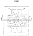
- Figure 2A is a plan view of the substrate of Figure 1A covered with a patterned sacrificial layer.
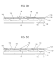
- Figure 2B is a cross sectional view of the substrate and sacrificial layer of Figure 2A taken along the section line labeled Fig. 2B.
- Figure 2C is a cross sectional view of the substrate and sacrificial layer of Figure 2A taken along the section line labeled Fig. 2C.
- Figure 3A is a plan view of the substrate and sacrificial layer of Figure 2A with supporting beams formed thereon.
- Figure 3B is a cross sectional view of the substrate of Figure 3A taken along the section line labeled Fig. 3B.
- Figure 3C is a cross sectional view of the substrate of Figure 3A taken along the section line labeled Fig. 3C.
- Figure 4A is a plan view of the substrate of Figure 3A with electrostatic actuators formed thereon.
- Figure 4B is a cross sectional view of the substrate of Figure 4A taken along the section line labeled Fig. 4B.
- Figure 4C is a cross sectional view of the substrate of Figure 4A taken along the section line labeled Fig. 4C.
- Figure 5A is a plan view of the substrate of Figure 4A after removing the sacrificial layers and sacrificial portions of the substrate.
- Figure 5B is a cross sectional view of the substrate of Figure 5A taken along the section line labeled Fig. 5B.
- Figure 5C is a cross sectional view of the substrate of Figure 5A taken along the section line labeled Fig. 5C.
- Figure 6 is a perspective view of an optical scanner according to the present invention.
- FIG. 5A A top view of a microelectromechanical rotating mirror according to the present invention is illustrated in Figure 5A, while cross sectional views are illustrated in Figures 5B and 5C.
- a first frame 50 and a second frame 52 respectively surround the rotating plate 54 on which a mirror can be formed.
- a first pair of beams 56 support the second frame 52 along a first axis relative to the first frame 50 so that the second frame 52 rotates about the first axis relative to the first frame 50 .
- a second pair of beams 58 supports the plate 54 along a second axis relative to the second frame 52 so that the plate 54 rotates about the second axis relative to the second frame 50 .
- the first axis of rotation and the second axis of rotation intersect at a 90° angle.
- a first set of four actuators 60 is provided on the first frame 50 with one actuator on each side of each of the beams 56 of the first pair. These actuators 60 provide mechanical force for rotating the second frame 52 relative to the first frame 50 about the first axis which is defined by the first pair of beams 56 .
- a second set of four actuators 62 is provided on the second frame 52 with one actuator on each side of each of the beams 58 of the second pair. These actuators 62 provide mechanical force for rotating the plate 54 relative to the second frame 52 about the second axis which is defined by the second pair of beams 58 .
- both sets of actuators assist in positioning and supporting the movable plate and second frame. Accordingly, the plate can rotate independently about both the first axis of rotation and the second axis of rotation.
- each of the beams 58 of the second pair extends from a side of the plate 54 and is fixedly connected thereto.
- Each beam 58 extends over the second frame 52 and is positioned adjacent the surface thereof for rotational movement. Accordingly, these beams 58 define the second axis of rotation about which the plate 54 rotates relative to the second frame 52 . Because the beams 58 are not fixedly connected to both the plate 54 and the second frame 52 , the torque required to rotate the plate about the second axis can be reduced. Furthermore, the arched contact surface 64 of each beam 58 adjacent the second frame 52 allows the beam to roll on the second frame during rotation of the plate 54 further reducing the torque required to rotate the plate.
- the arched contact surface 64 can be rounded, pointed, or otherwise shaped to provide a rolling motion for the beam when the plate rotates.
- the pair of second beams extending from opposite sides of the plate is defined to include a structure wherein the pair of beams are joined on the plate.
- the pair of second beams can be provided by a structure on the plate which extends across the plate and beyond opposite sides of the plate.
- the pair of first beams can be provided by a similar structure on the second frame raised to permit movement of the plate.
- the pair of second beams and the plate can be formed from a single layer of a material such as polysilicon so that the pair of second beams and the plate are confined within a single plane.
- the pair of first beams and the second frame can similarly be formed from a single layer.
- the beams 56 extending from the second frame 52 operate in the same manner as discussed above with regard to the beams 58 extending from the plate 54 .
- each of the actuators 62 includes at least one electrode 66 spaced apart from and electrically insulated from the second frame 52 , and an arm 68 extending from the electrode 66 and attached to a portion of the plate 54 off the second axis.
- the electrode is an electrically conductive plate generally parallel to the second frame and spaced from it by supports, as illustrated in Figures 5B and 5C.
- the supports are preferably located at the edge of the electrode and are located on two sides, but this configuration may change as necessary or desirable to obtain the optimum combination of structural support and flexibility for movement.
- a potential difference between the electrode 66 and the second frame 52 will result in an electrostatic force which is transmitted via the arm 68 to the plate 54 thus rotating the plate 54 relative to the second frame 52 .
- the actuator 62 can thus provide a structure that supports the plate 54 relative to the second frame 52 and selectively biases it to induce desired rotation.
- Such biasing support can alternately be provided by micromachined springs which can be formed from the same material used to form the plate and the second frame. For example, serpentine springs may be formed between the plate and frame.
- the rotation of the second frame 52 is illustrated by arrows 59 in Figures 5B and 5C. This rotation occurs in the plane of Figures 5B and 5C about the axis defined by the first pair of beams 56 (shown in Figure 5A).
- the plate 54 rotates into and out of the plane of Figures 5B and 5C about the axis defined by the second pair of beams 58 .
- the electrode 66 By generating a potential difference between the electrode 66 and the second frame 52 at a location remote from the plate or its rotational arc, the electrode does not interfere with or intrude into the path of rotation of the plate 54 . Accordingly, the electrode 66 can be closely spaced from the second frame 52 thus increasing the electrostatic force generated without reducing a range of motion for the plate 54 . Furthermore, the useful size of the electrode 62 and the electrostatic forces generated thereby are not limited by the size of the plate 54 .
- the arm 68 preferably extends to a portion of the plate 54 closely spaced from the second axis. Accordingly, a relatively small displacement of the arm 68 can result in a relatively large rotation of the plate 54 .
- the actuator arms 68 are fixedly connected to the plate 54 thus providing biasing support for the plate.
- the arms can extend adjacent to the plate without being fixedly connected thereto. Accordingly, the torque required to rotate the plate can be reduced because the arms are positioned adjacent the surface of the plate but are not attached to it.
- the insulating layer 110 forming the upper surface of the second frame can be used to prevent electrical shorts between the electrode 62 and the conductive portion of the second frame 52 .
- the actuators 60 on the first frame including electrodes 70 and the arms 72 operate as discussed above with regard to the actuators 62 on the second frame.
- a rotating mirror By providing a reflective surface 107 on the plate, a rotating mirror is produced.
- This rotating mirror can be used to provide an optical scanner 200 such as a bar code reader, as shown in Figure 6.
- a laser 202 or other energy source can generate a beam of electromagnetic radiation 204 such as light and project the beam onto the reflective surface 107 of the rotating mirror.
- the reflected beam 206 By rotating the mirror about the first and second axes, the reflected beam 206 can be scanned in a predetermined pattern. This scanned beam can be used to read a pattern such as a bar code.
- the control circuit 208 may provide control signals which control the operation of the rotating mirror and the operation of the laser.
- predetermined surface regions of substrate 100 are doped thus defining the first frame region 102 , the second frame region 104 , and the plate region 106 .
- the substrate can be a microelectronic substrate formed from materials such as silicon, gallium arsenide, or other materials used in the fabrication of microelectronic devices.
- the predetermined surface regions can be doped with boron by either an implant or a diffusion step. Each of these regions is separated by sacrificial substrate regions 108 .
- the dopant can later serve as an etch stop so that the sacrificial regions of the substrate can be selectively etched away leaving only doped portions of the substrate.
- Such an etch can be performed at a later point in fabrication to separate the first frame 50 , the second frame 52 , and the plate 54 as shown in Figures 5A-C. Accordingly, the frame and plate regions can be defined without creating significant topology which could increase the difficulty of processing.
- a protective nitride layer 110 can be formed on the doped regions of the substrate, and a sacrificial layer 112 can then be formed on the substrate and patterned, as shown in Figures 2A-C.
- the nitride layer 110 can provide stress compensation in the frame and plate regions when separated, and the nitride layer 110 can also provide an insulating layer between the electrodes and respective frames.
- the nitride layer 110 can also provide insulation between conductive lines and the doped regions of the substrate. Alternately, the nitride layer 110 can cover only portions of the doped regions as required. For example, portions of the plate could be left uncovered using the reflective properties of the substrate to provide the mirror.
- a protective nitride layer 111 can also be formed on the back of the substrate 100 . The nitride layers 110 and 111 can be formed simultaneously.
- Partial holes 126 in the sacrificial layer provide a mold for the arched contact surfaces for each of the first pair of beams
- the partial holes 128 provide a mold for the arched contact surfaces for each of the second pair of beams.
- the partial holes 126 and 128 can be formed simultaneously by isotropically etching partial holes through the sacrificial layer 112 without exposing the substrate.
- the isotropic etch provides the arched surfaces shown in Figure 2B.
- small portions of the sacrificial layer 112 are exposed photolithographically, and a wet isotropic etch is performed for a predetermined time so that the partial hole is formed with the arched surface and without exposing the substrate.
- the sacrificial layer 112 can include a first sacrificial sublayer 112A having a first etch rate and a second sacrificial sublayer 112B having a second etch rate which is high relative to the first etch rate. Accordingly, the partial hole is formed primarily in the second sacrificial sublayer 112B with the first sacrificial sublayer 112A being used to prevent the substrate from being exposed.
- the first sacrificial sublayer 112A can be formed from a thermal silicon oxide
- the second sacrificial sublayer 112B can be formed from phosphorus silicate glass (PSG) which has an etch rate that is high when compared to that of a thermal silicon oxide. Accordingly, a portion of the sacrificial layer remains between the arched surface of the partial holes and the substrate. Dashed lines in Figure 2A indicate the frame and plate regions of the substrate which have been previously defined and covered with the sacrificial layer 112 .
- the sacrificial layer 112 can then be patterned to expose portions of the substrate to which the actuators and supporting beams will be anchored.
- the holes 114 expose portions of the substrate to which the first pair of beams will be anchored to the second frame.
- the holes 116 expose portions of the substrate to which the second pair of beams will be anchored to the plate.
- the holes 118 expose portions of the substrate to which the first set of actuator electrodes will be anchored to the first frame, and the holes 120 expose portions of the substrate to which the first set of actuator arms will be anchored to the second frame.
- the holes 122 expose portions of the substrate to which the second set of actuator electrodes will be anchored to the second frame, and holes 124 expose portions of the substrate to which the second set of actuator arms will be anchored to the plate.
- the step of forming the partial holes 126 and 128 precedes the step of forming the holes 114, 116, 118, 120, 122 , and 124 which expose the substrate because higher resolution patterning may be required to form
- the actuator electrodes can be anchored to the substrate along L shaped patterns 118 and 122 as shown in Figure 2A.
- the actuator electrodes can be anchored to smaller portions of the substrate such as patterns including only the linear portion of the L perpendicular to the respective axis of rotation.
- the larger L shaped anchor may provide a stiffer actuator capable of providing lower force at a higher frequency of operation, while the smaller linear anchor may provide a more flexible actuator capable of providing greater force at a lower frequency of operation.
- a polysilicon layer is formed on the patterned sacrificial layer 112 and patterned to form the beams which define the axes of rotation and to form the anchoring structures for the actuator electrodes and arms, as shown in Figures 3A-C.
- each of the beams 56 fills a respective hole 114 fixedly connecting it to the second frame region of the substrate and extends to the respective partial hole 126 thus forming the arched contact surface spaced from the first frame region of the substrate.
- Each of the beams 58 fills a respective hole 116 fixedly connecting it to the plate region of the substrate and extends to the respective partial hole 128 thus forming the arched contact surface spaced from the second frame region of the substrate.
- Anchoring structures 130, 132, 134 , and 136 are also formed from this patterned layer of polysilicon.
- Anchoring structures 130 are used to anchor the electrodes of the first set of actuators to the first frame region of the substrate, and anchoring structures 132 are used to anchor the electrodes from the second set of actuators to the second frame portion of the substrate.
- Anchoring structures 134 are used to anchor the arms from the first set of actuators to the second frame region of the substrate, and anchoring structures 136 are used to anchor the arms from the second set of actuators to the plate region of the substrate.
- the relatively large L shaped anchoring structures 130 and 132 can be used to provide relatively stiff actuators.
- a second sacrificial layer 140 is then formed on the structure of Figures 3A-C and patterned, and a second patterned polysilicon layer is formed thereon as shown in Figures 4A-C.
- the second sacrificial layer 140 is patterned to expose the anchoring structures 130, 132, 134 , and 136 shown in Figures 3A-3C. Because the polysilicon beams 56 and 58 are covered by the second polysilicon layer 140 , these beams are illustrated with dotted lines in Figure 4A. As before, the defined regions of the substrate are also illustrated with dotted lines.
- the second patterned polysilicon layer forms the actuators 60 including electrodes 70 and arms 72 , and the actuators 62 including electrodes 66 and arms 68 .
- the second patterned polysilicon layer can be heavily doped so that the electrode portion of the actuator is conductive.
- the actuators 60 and 62 are formed on the respective anchoring structures 130, 134, 132 , and 136 which are exposed by the second sacrificial layer.
- the first polysilicon layer is relatively thick so that the beams 56 and 58 are stiff, and the second polysilicon layer is relatively thin so that the electrodes of the actuators are relatively flexible.
- the beams can be formed from a polysilicon layer on the order of several microns thick, and the electrodes can be formed from polysilicon on the order of less than one micron thick.
- the beams and the electrodes can be formed from the same polysilicon layer thus eliminating the need to form and pattern the second sacrificial layer and the second polysilicon layer.
- the spacing between the actuator electrode and the substrate is determined by the combined thicknesses of the sacrificial layers. Accordingly, this spacing can be precisely controlled, and very small spacings can be provided.
- the sacrificial layers and the sacrificial portions of the substrate are then selectively removed to form the microelectromechanical rotating mirror shown in Figures 5A-C.
- the backside nitride layer 111 is patterned to provide a mask for etching the substrate 100 using an etchant such as KOH to remove the undoped and unmasked portions of the substrate. Accordingly, the second frame region 104 is separated from the first frame region 102 , and the plate region 106 is separated from the second frame region 104 , thus forming the first frame 50 , the second frame 52 , and the plate 54 .
- the sacrificial layers 112 and 140 are then selectively removed using an etchant such as HF to free the cantilevered actuator arms and support beams.
- the second frame 52 is suspended relative to the first frame 50 by the actuators 60 .
- the plate 54 is suspended relative to the second frame 52 by the actuators 62 .
- the beams 58 thus include arched contact surfaces 64 adjacent the second frame 52 so that each beam is in rotational contact with the second frame.
- the contact surfaces of both of the beams can be slightly spaced from the second frame 52 .
- the contact surface comes into contact with the second frame forcing the plate to then rotate about the axis defined by the beams. Accordingly, the beam rolls relative to the frame reducing the torque required to rotate the plate.
- the beam is thus defined as being in rotational contact with the frame even though a narrow space may exist between the contact surface of the beam and the frame when no force is applied to the plate.
- the electrodes of the actuators can be closely spaced from the second frame thus increasing the electrostatic force generated thereby while still effecting a significant rotation of the plate.
- the actuators are illustrated with the rotating beams, the actuator can alternately be used with other means for defining the axis of rotation.
- the actuator can be used with torsion bars and/or a supporting ridge.
- the rotating beams are illustrated with the electrostatic actuatcrs, the rotating beams can be used with other actuators.
- the rotating beams can be used together with thermal actuators, magnetic actuators, piezoelectric actuators, and bimetallic actuators.
- the plate 54 can serve as the mirror. If the substrate is a polished single crystal semiconductor material, a mirror finish can be provided by removing a portion of the nitride layer therefrom. Alternately, a layer 107 of a reflective material such as a metal can be formed on the plate. According to yet another alternative, the plate can be formed from the first polysilicon layer used to form the beams and polished or otherwise provided with a reflective layer thereon. The plate and the beams can thus be formed as an integrated structure.
- Electrical connections on each of the first frame, the second frame, and the plate can be provided by conductive lines thereon.
- metal lines or doped polysilicon lines can provide interconnection, and these lines can be insulated from the doped silicon by the nitride layer 110 .
- Electrical connection between the first and second frames can be provided by wire bonding, through electrical connection across the beams 56 , through electrical connection across the actuator arms 72 , or through electrical connection across a long flexible bridge structure between the first and second frames.
- microelectromechanical rotating mirror of Figures 5A-C can thus be formed on a single substrate without the need to bond wafers or assemble discrete components. Accordingly, this mirror can be economically and reliably fabricated. Furthermore, the mirror provides independent rotation about two axes, and the electrodes do not lie in the path of rotations of the mirror.
- subsequent processing can be performed on a smooth substrate.
- the subsequent processes can be performed more easily due to the reduction in topography.
- Significant topography is added to the structure only after the final etches removing the sacrificial layers and substrate regions which occur after most processes which are sensitive to extreme topography have been completed.
Landscapes
- Physics & Mathematics (AREA)
- General Physics & Mathematics (AREA)
- Optics & Photonics (AREA)
- Engineering & Computer Science (AREA)
- Computer Hardware Design (AREA)
- Microelectronics & Electronic Packaging (AREA)
- Health & Medical Sciences (AREA)
- Life Sciences & Earth Sciences (AREA)
- Chemical & Material Sciences (AREA)
- Analytical Chemistry (AREA)
- Biochemistry (AREA)
- General Health & Medical Sciences (AREA)
- Immunology (AREA)
- Pathology (AREA)
- Micromachines (AREA)
- Mechanical Light Control Or Optical Switches (AREA)
- Mechanical Optical Scanning Systems (AREA)
Applications Claiming Priority (2)
| Application Number | Priority Date | Filing Date | Title |
|---|---|---|---|
| US719711 | 1991-06-26 | ||
| US08/719,711 US5914801A (en) | 1996-09-27 | 1996-09-27 | Microelectromechanical devices including rotating plates and related methods |
Publications (2)
| Publication Number | Publication Date |
|---|---|
| EP0834759A2 true EP0834759A2 (de) | 1998-04-08 |
| EP0834759A3 EP0834759A3 (de) | 1999-10-13 |
Family
ID=24891063
Family Applications (1)
| Application Number | Title | Priority Date | Filing Date |
|---|---|---|---|
| EP97307510A Withdrawn EP0834759A3 (de) | 1996-09-27 | 1997-09-25 | Mikroelektromechanische Geräte mit rotierenden Platten und zugehörige Verfahren |
Country Status (5)
| Country | Link |
|---|---|
| US (5) | US5914801A (de) |
| EP (1) | EP0834759A3 (de) |
| JP (1) | JPH10323059A (de) |
| KR (1) | KR19980025006A (de) |
| TW (1) | TW387159B (de) |
Cited By (32)
| Publication number | Priority date | Publication date | Assignee | Title |
|---|---|---|---|---|
| US6044705A (en) * | 1993-10-18 | 2000-04-04 | Xros, Inc. | Micromachined members coupled for relative rotation by torsion bars |
| WO2001056919A3 (en) * | 2000-02-01 | 2002-03-28 | Calient Networks Inc | Micro-electro-mechanical-system (mems) mirror device and methods for fabricating the same |
| WO2002012116A3 (en) * | 2000-08-03 | 2002-04-04 | Analog Devices Inc | Bonded wafer optical mems process |
| WO2001094253A3 (en) * | 2000-06-02 | 2002-04-04 | Calient Networks Inc | Bulk silicon structures with thin film flexible elements |
| US6373682B1 (en) | 1999-12-15 | 2002-04-16 | Mcnc | Electrostatically controlled variable capacitor |
| US6377438B1 (en) | 2000-10-23 | 2002-04-23 | Mcnc | Hybrid microelectromechanical system tunable capacitor and associated fabrication methods |
| US6396620B1 (en) | 2000-10-30 | 2002-05-28 | Mcnc | Electrostatically actuated electromagnetic radiation shutter |
| WO2002006152A3 (en) * | 2000-07-14 | 2002-07-11 | Zyvex Corp | System and method for constraining totally released microcomponents |
| US6426013B1 (en) | 1993-10-18 | 2002-07-30 | Xros, Inc. | Method for fabricating micromachined members coupled for relative rotation |
| FR2820834A1 (fr) * | 2001-02-15 | 2002-08-16 | Teem Photonics | Procede de fabrication d'un micro-miroir optique et micro-miroir ou matrice de micro-miroirs obtenu par ce procede |
| US6467345B1 (en) | 1993-10-18 | 2002-10-22 | Xros, Inc. | Method of operating micromachined members coupled for relative rotation |
| GB2375185A (en) * | 2001-05-04 | 2002-11-06 | Kymata Ltd | Thick wafer for MEMS fabrication |
| US6485273B1 (en) | 2000-09-01 | 2002-11-26 | Mcnc | Distributed MEMS electrostatic pumping devices |
| US6544863B1 (en) | 2001-08-21 | 2003-04-08 | Calient Networks, Inc. | Method of fabricating semiconductor wafers having multiple height subsurface layers |
| WO2002037162A3 (en) * | 2000-10-31 | 2003-05-01 | 3M Innovative Properties Co | Gimbaled micro-mirror positionable by thermal actuators |
| US6560384B1 (en) | 2000-06-01 | 2003-05-06 | Calient Networks, Inc. | Optical switch having mirrors arranged to accommodate freedom of movement |
| US6578974B2 (en) | 2000-05-18 | 2003-06-17 | Calient Networks, Inc. | Micromachined apparatus for improved reflection of light |
| US6586738B2 (en) | 2001-04-13 | 2003-07-01 | Mcnc | Electromagnetic radiation detectors having a micromachined electrostatic chopper device |
| US6587611B1 (en) | 2000-06-06 | 2003-07-01 | Calient Networks, Inc. | Maintaining path integrity in an optical switch |
| US6610974B1 (en) | 2000-06-05 | 2003-08-26 | Calient Networks, Inc. | Positioning a movable reflector in an optical switch |
| US6628041B2 (en) | 2000-05-16 | 2003-09-30 | Calient Networks, Inc. | Micro-electro-mechanical-system (MEMS) mirror device having large angle out of plane motion using shaped combed finger actuators and method for fabricating the same |
| US6643425B1 (en) | 2000-08-17 | 2003-11-04 | Calient Networks, Inc. | Optical switch having switch mirror arrays controlled by scanning beams |
| US6714700B2 (en) | 2000-04-16 | 2004-03-30 | Avanex Corporation | Micro electromechanical system and method for transmissively switching optical signals |
| US6728016B1 (en) | 2000-06-05 | 2004-04-27 | Calient Networks, Inc. | Safe procedure for moving mirrors in an optical cross-connect switch |
| US6753638B2 (en) | 2000-02-03 | 2004-06-22 | Calient Networks, Inc. | Electrostatic actuator for micromechanical systems |
| US6792177B2 (en) | 2001-03-12 | 2004-09-14 | Calient Networks, Inc. | Optical switch with internal monitoring |
| US6825967B1 (en) | 2000-09-29 | 2004-11-30 | Calient Networks, Inc. | Shaped electrodes for micro-electro-mechanical-system (MEMS) devices to improve actuator performance and methods for fabricating the same |
| US6964894B2 (en) | 2003-06-23 | 2005-11-15 | Analog Devices, Inc. | Apparatus and method of forming a device layer |
| US7026602B2 (en) | 2001-04-13 | 2006-04-11 | Research Triangle Institute | Electromagnetic radiation detectors having a microelectromechanical shutter device |
| US7110633B1 (en) | 2001-08-13 | 2006-09-19 | Calient Networks, Inc. | Method and apparatus to provide alternative paths for optical protection path switch arrays |
| US7906359B2 (en) | 2002-12-03 | 2011-03-15 | Analog Devices, Inc. | Method of forming a surface micromachined MEMS device |
| CN103095976A (zh) * | 2013-01-15 | 2013-05-08 | 广东欧珀移动通信有限公司 | Mems摄像头光圈控制装置及其应用的mems摄像头 |
Families Citing this family (176)
| Publication number | Priority date | Publication date | Assignee | Title |
|---|---|---|---|---|
| US5914801A (en) * | 1996-09-27 | 1999-06-22 | Mcnc | Microelectromechanical devices including rotating plates and related methods |
| US6786420B1 (en) | 1997-07-15 | 2004-09-07 | Silverbrook Research Pty. Ltd. | Data distribution mechanism in the form of ink dots on cards |
| US6618117B2 (en) | 1997-07-12 | 2003-09-09 | Silverbrook Research Pty Ltd | Image sensing apparatus including a microcontroller |
| AUPO798697A0 (en) * | 1997-07-15 | 1997-08-07 | Silverbrook Research Pty Ltd | Data processing method and apparatus (ART51) |
| AUPO802797A0 (en) | 1997-07-15 | 1997-08-07 | Silverbrook Research Pty Ltd | Image processing method and apparatus (ART54) |
| US6985207B2 (en) | 1997-07-15 | 2006-01-10 | Silverbrook Research Pty Ltd | Photographic prints having magnetically recordable media |
| US6690419B1 (en) | 1997-07-15 | 2004-02-10 | Silverbrook Research Pty Ltd | Utilising eye detection methods for image processing in a digital image camera |
| US6682174B2 (en) | 1998-03-25 | 2004-01-27 | Silverbrook Research Pty Ltd | Ink jet nozzle arrangement configuration |
| AUPO850597A0 (en) | 1997-08-11 | 1997-09-04 | Silverbrook Research Pty Ltd | Image processing method and apparatus (art01a) |
| US6879341B1 (en) | 1997-07-15 | 2005-04-12 | Silverbrook Research Pty Ltd | Digital camera system containing a VLIW vector processor |
| US7110024B1 (en) | 1997-07-15 | 2006-09-19 | Silverbrook Research Pty Ltd | Digital camera system having motion deblurring means |
| US7556356B1 (en) | 1997-07-15 | 2009-07-07 | Silverbrook Research Pty Ltd | Inkjet printhead integrated circuit with ink spread prevention |
| US6712453B2 (en) | 1997-07-15 | 2004-03-30 | Silverbrook Research Pty Ltd. | Ink jet nozzle rim |
| US7337532B2 (en) | 1997-07-15 | 2008-03-04 | Silverbrook Research Pty Ltd | Method of manufacturing micro-electromechanical device having motion-transmitting structure |
| US20040119829A1 (en) | 1997-07-15 | 2004-06-24 | Silverbrook Research Pty Ltd | Printhead assembly for a print on demand digital camera system |
| US6188415B1 (en) | 1997-07-15 | 2001-02-13 | Silverbrook Research Pty Ltd | Ink jet printer having a thermal actuator comprising an external coil spring |
| US6935724B2 (en) | 1997-07-15 | 2005-08-30 | Silverbrook Research Pty Ltd | Ink jet nozzle having actuator with anchor positioned between nozzle chamber and actuator connection point |
| US7468139B2 (en) | 1997-07-15 | 2008-12-23 | Silverbrook Research Pty Ltd | Method of depositing heater material over a photoresist scaffold |
| US6624848B1 (en) | 1997-07-15 | 2003-09-23 | Silverbrook Research Pty Ltd | Cascading image modification using multiple digital cameras incorporating image processing |
| US6641315B2 (en) * | 1997-07-15 | 2003-11-04 | Silverbrook Research Pty Ltd | Keyboard |
| US7195339B2 (en) | 1997-07-15 | 2007-03-27 | Silverbrook Research Pty Ltd | Ink jet nozzle assembly with a thermal bend actuator |
| US6648453B2 (en) | 1997-07-15 | 2003-11-18 | Silverbrook Research Pty Ltd | Ink jet printhead chip with predetermined micro-electromechanical systems height |
| US7465030B2 (en) | 1997-07-15 | 2008-12-16 | Silverbrook Research Pty Ltd | Nozzle arrangement with a magnetic field generator |
| US6201629B1 (en) | 1997-08-27 | 2001-03-13 | Microoptical Corporation | Torsional micro-mechanical mirror system |
| US6074890A (en) * | 1998-01-08 | 2000-06-13 | Rockwell Science Center, Llc | Method of fabricating suspended single crystal silicon micro electro mechanical system (MEMS) devices |
| US6872984B1 (en) | 1998-07-29 | 2005-03-29 | Silicon Light Machines Corporation | Method of sealing a hermetic lid to a semiconductor die at an angle |
| US6303986B1 (en) | 1998-07-29 | 2001-10-16 | Silicon Light Machines | Method of and apparatus for sealing an hermetic lid to a semiconductor die |
| US7098871B1 (en) * | 1998-08-05 | 2006-08-29 | Microvision, Inc. | Optical scanning system with correction |
| AUPP702098A0 (en) | 1998-11-09 | 1998-12-03 | Silverbrook Research Pty Ltd | Image creation method and apparatus (ART73) |
| US6014257A (en) * | 1998-10-14 | 2000-01-11 | Eastman Kodak Company | Light modulator |
| US5991079A (en) * | 1998-10-14 | 1999-11-23 | Eastman Kodak Company | Method of making a light modulator |
| US6088148A (en) * | 1998-10-30 | 2000-07-11 | Eastman Kodak Company | Micromagnetic light modulator |
| AU3756300A (en) | 1999-03-18 | 2000-10-04 | Trustees Of Boston University | Very large angle integrated optical scanner made with an array of piezoelectric monomorphs |
| US6428173B1 (en) * | 1999-05-03 | 2002-08-06 | Jds Uniphase, Inc. | Moveable microelectromechanical mirror structures and associated methods |
| AUPQ056099A0 (en) | 1999-05-25 | 1999-06-17 | Silverbrook Research Pty Ltd | A method and apparatus (pprint01) |
| US6315423B1 (en) * | 1999-07-13 | 2001-11-13 | Input/Output, Inc. | Micro machined mirror |
| US6617098B1 (en) | 1999-07-13 | 2003-09-09 | Input/Output, Inc. | Merged-mask micro-machining process |
| DE69933370D1 (de) * | 1999-07-15 | 2006-11-09 | St Microelectronics Srl | Verfahren zur Zusammenstellung einer Gruppe, die zumindest ein erstes und ein zweites Element aufweist, wobei eines der Elemente eine Mikrostruktur ohne Verpackung umfasst |
| EP1218790A2 (de) * | 1999-07-20 | 2002-07-03 | Memlink Ltd. | Mikroelekromechanische vorrichtung mit beweglichem element |
| US6535663B1 (en) * | 1999-07-20 | 2003-03-18 | Memlink Ltd. | Microelectromechanical device with moving element |
| US6268635B1 (en) | 1999-08-04 | 2001-07-31 | Jds Uniphase Inc. | Dielectric links for microelectromechanical systems |
| US6653621B2 (en) * | 2001-03-23 | 2003-11-25 | Microvision, Inc. | Frequency tunable resonant scanner and method of making |
| US6924476B2 (en) * | 2002-11-25 | 2005-08-02 | Microvision, Inc. | Resonant beam scanner with raster pinch compensation |
| US6433907B1 (en) * | 1999-08-05 | 2002-08-13 | Microvision, Inc. | Scanned display with plurality of scanning assemblies |
| US6211598B1 (en) * | 1999-09-13 | 2001-04-03 | Jds Uniphase Inc. | In-plane MEMS thermal actuator and associated fabrication methods |
| US6445844B1 (en) * | 1999-09-15 | 2002-09-03 | Xros, Inc. | Flexible, modular, compact fiber optic switch |
| US6201631B1 (en) | 1999-10-08 | 2001-03-13 | Lucent Technologies Inc. | Process for fabricating an optical mirror array |
| US7225809B1 (en) | 1999-11-01 | 2007-06-05 | Ric Investments, Llc | Method and apparatus for monitoring and controlling a medical device |
| US6535318B1 (en) * | 1999-11-12 | 2003-03-18 | Jds Uniphase Corporation | Integrated optoelectronic devices having pop-up mirrors therein and methods of forming and operating same |
| US6658177B1 (en) | 1999-12-13 | 2003-12-02 | Memlink Ltd. | Switching device and method of fabricating the same |
| US6541831B2 (en) | 2000-01-18 | 2003-04-01 | Cornell Research Foundation, Inc. | Single crystal silicon micromirror and array |
| US6956878B1 (en) | 2000-02-07 | 2005-10-18 | Silicon Light Machines Corporation | Method and apparatus for reducing laser speckle using polarization averaging |
| US6586841B1 (en) | 2000-02-23 | 2003-07-01 | Onix Microsystems, Inc. | Mechanical landing pad formed on the underside of a MEMS device |
| US6351580B1 (en) | 2000-03-27 | 2002-02-26 | Jds Uniphase Corporation | Microelectromechanical devices having brake assemblies therein to control movement of optical shutters and other movable elements |
| US6310419B1 (en) | 2000-04-05 | 2001-10-30 | Jds Uniphase Inc. | Resistor array devices including switch contacts operated by microelectromechanical actuators and methods for fabricating the same |
| US6628856B1 (en) | 2000-09-27 | 2003-09-30 | Dicon Fiberoptics, Inc. | Optical switch |
| US6567574B1 (en) | 2000-10-06 | 2003-05-20 | Omm, Inc. | Modular three-dimensional optical switch |
| US6600849B2 (en) | 2000-11-20 | 2003-07-29 | Jds Uniphase Inc. | Control system for optical cross-connect switches |
| US7039267B2 (en) * | 2000-11-20 | 2006-05-02 | Jds Uniphase Inc. | Optical switch |
| US6560000B2 (en) | 2000-11-20 | 2003-05-06 | Jds Uniphase Inc. | Wavelength-dependent optical signal processing using an angle-to-offset module |
| CA2328759A1 (en) * | 2000-11-20 | 2002-05-20 | Thomas Ducellier | Optical switch |
| CA2326362A1 (en) | 2000-11-20 | 2002-05-20 | Thomas Ducellier | Optical switch |
| CA2327862A1 (en) | 2000-11-20 | 2002-05-20 | Thomas Ducellier | Optical switch |
| JP4723719B2 (ja) * | 2000-11-30 | 2011-07-13 | オリンパス株式会社 | ガルバノミラー装置 |
| US6808956B2 (en) | 2000-12-27 | 2004-10-26 | Honeywell International Inc. | Thin micromachined structures |
| US6582985B2 (en) | 2000-12-27 | 2003-06-24 | Honeywell International Inc. | SOI/glass process for forming thin silicon micromachined structures |
| US6711318B2 (en) | 2001-01-29 | 2004-03-23 | 3M Innovative Properties Company | Optical switch based on rotating vertical micro-mirror |
| US6480320B2 (en) * | 2001-02-07 | 2002-11-12 | Transparent Optical, Inc. | Microelectromechanical mirror and mirror array |
| US6803843B2 (en) * | 2001-02-22 | 2004-10-12 | Canon Kabushiki Kaisha | Movable-body apparatus, optical deflector, and method of fabricating the same |
| US6491404B2 (en) | 2001-02-23 | 2002-12-10 | Jds Uniphase Corporation | Microelectromechanical apparatus with tiltable bodies including variable tilt-stop engaging portions and methods of operation and fabrication therefor |
| US7183633B2 (en) * | 2001-03-01 | 2007-02-27 | Analog Devices Inc. | Optical cross-connect system |
| US7177081B2 (en) | 2001-03-08 | 2007-02-13 | Silicon Light Machines Corporation | High contrast grating light valve type device |
| US6970616B2 (en) * | 2001-03-18 | 2005-11-29 | Touchdown Technologies, Inc. | Optical cross-connect assembly |
| US6707591B2 (en) | 2001-04-10 | 2004-03-16 | Silicon Light Machines | Angled illumination for a single order light modulator based projection system |
| US6438954B1 (en) * | 2001-04-27 | 2002-08-27 | 3M Innovative Properties Company | Multi-directional thermal actuator |
| US6757093B2 (en) | 2001-05-21 | 2004-06-29 | Jds Uniphase Corporation | MEMS reflectors having tail portions that extend inside a recess and head portions that extend outside the recess and methods of forming same |
| US6851425B2 (en) | 2001-05-25 | 2005-02-08 | Respironics, Inc. | Exhaust port assembly for a pressure support system |
| ITTO20010519A1 (it) * | 2001-05-31 | 2002-12-01 | St Microelectronics Srl | Dispositivo orientabile, in particolare dispositivo attuatore di dischi rigidi, con controllo dell'angolo di rollio e di beccheggio. |
| US6865346B1 (en) | 2001-06-05 | 2005-03-08 | Silicon Light Machines Corporation | Fiber optic transceiver |
| US6747781B2 (en) | 2001-06-25 | 2004-06-08 | Silicon Light Machines, Inc. | Method, apparatus, and diffuser for reducing laser speckle |
| US6782205B2 (en) | 2001-06-25 | 2004-08-24 | Silicon Light Machines | Method and apparatus for dynamic equalization in wavelength division multiplexing |
| JP2003015064A (ja) * | 2001-07-04 | 2003-01-15 | Fujitsu Ltd | マイクロミラー素子 |
| CA2394936C (en) | 2001-07-25 | 2011-12-13 | Jds Uniphase Inc. | Wavelength cross-connect |
| US6829092B2 (en) | 2001-08-15 | 2004-12-07 | Silicon Light Machines, Inc. | Blazed grating light valve |
| US6782153B2 (en) | 2001-08-28 | 2004-08-24 | Dicon Fiberoptics, Inc. | Hybrid opto-mechanical component |
| US6930364B2 (en) | 2001-09-13 | 2005-08-16 | Silicon Light Machines Corporation | Microelectronic mechanical system and methods |
| US6677695B2 (en) * | 2001-09-18 | 2004-01-13 | Jds Uniphase Corporation | MEMS electrostatic actuators with reduced actuation voltage |
| ATE393409T1 (de) * | 2001-10-19 | 2008-05-15 | Ion Geophysical Corp | Digitale optische schaltvorrichtung und prozess zu ihrer herstellung |
| US7190509B2 (en) * | 2001-11-07 | 2007-03-13 | Trex Enterprises Corp. | Optically addressed MEMS |
| ATE417021T1 (de) | 2001-11-09 | 2008-12-15 | Wispry Inc | Mems-einrichtung mit dreischichtigem strahl und diesbezügliche verfahren |
| US6956995B1 (en) | 2001-11-09 | 2005-10-18 | Silicon Light Machines Corporation | Optical communication arrangement |
| WO2003045837A2 (en) * | 2001-11-26 | 2003-06-05 | Wisconsin Alumni Research Foundation | Stress control of semiconductor microstructures for thin film growth |
| US7372616B2 (en) * | 2001-12-06 | 2008-05-13 | Microfabrica, Inc. | Complex microdevices and apparatus and methods for fabricating such devices |
| US7244367B2 (en) * | 2001-12-11 | 2007-07-17 | Jds Uniphase Corporation | Metal alloy elements in micromachined devices |
| US7872394B1 (en) | 2001-12-13 | 2011-01-18 | Joseph E Ford | MEMS device with two axes comb drive actuators |
| US6745567B1 (en) | 2001-12-28 | 2004-06-08 | Zyvex Corporation | System and method for positional movement of microcomponents |
| US6973365B1 (en) | 2001-12-28 | 2005-12-06 | Zyvex Corporation | System and method for handling microcomponent parts for performing assembly of micro-devices |
| US6800238B1 (en) | 2002-01-15 | 2004-10-05 | Silicon Light Machines, Inc. | Method for domain patterning in low coercive field ferroelectrics |
| KR100447214B1 (ko) * | 2002-02-08 | 2004-09-04 | 엘지전자 주식회사 | 마이크로 미러 |
| US6954301B2 (en) * | 2002-04-30 | 2005-10-11 | The Regents Of The University Of Michigan | Low-voltage electromechanical device including a tiltable microplatform, method of tilting same, array of such devices and method of setting dimple-to-substrate spacing |
| US6767751B2 (en) | 2002-05-28 | 2004-07-27 | Silicon Light Machines, Inc. | Integrated driver process flow |
| US6728023B1 (en) | 2002-05-28 | 2004-04-27 | Silicon Light Machines | Optical device arrays with optimized image resolution |
| US7054515B1 (en) | 2002-05-30 | 2006-05-30 | Silicon Light Machines Corporation | Diffractive light modulator-based dynamic equalizer with integrated spectral monitor |
| US6822797B1 (en) | 2002-05-31 | 2004-11-23 | Silicon Light Machines, Inc. | Light modulator structure for producing high-contrast operation using zero-order light |
| JP3987382B2 (ja) * | 2002-06-11 | 2007-10-10 | 富士通株式会社 | マイクロミラー素子およびその製造方法 |
| US6829258B1 (en) | 2002-06-26 | 2004-12-07 | Silicon Light Machines, Inc. | Rapidly tunable external cavity laser |
| US6714337B1 (en) | 2002-06-28 | 2004-03-30 | Silicon Light Machines | Method and device for modulating a light beam and having an improved gamma response |
| US6813059B2 (en) | 2002-06-28 | 2004-11-02 | Silicon Light Machines, Inc. | Reduced formation of asperities in contact micro-structures |
| US6908201B2 (en) | 2002-06-28 | 2005-06-21 | Silicon Light Machines Corporation | Micro-support structures |
| AU2003263841A1 (en) * | 2002-08-01 | 2004-02-23 | Georgia Tech Research Corporation | Piezo electric on seminconductor on- insulator resonator |
| US6807334B2 (en) * | 2002-08-06 | 2004-10-19 | Agilent Technologies, Inc. | Optical switching system, optical switch, and electro-optical mechanical device |
| WO2004027796A2 (en) * | 2002-08-07 | 2004-04-01 | Georgia Tech Research Corporation | Capacitive resonators and methods of fabrication |
| KR100469062B1 (ko) | 2002-08-13 | 2005-02-02 | 한국전자통신연구원 | 광통신용 주사 미세거울 및 그 제조 방법 |
| US6801354B1 (en) | 2002-08-20 | 2004-10-05 | Silicon Light Machines, Inc. | 2-D diffraction grating for substantially eliminating polarization dependent losses |
| US6843574B2 (en) * | 2002-08-20 | 2005-01-18 | Intel Corporation | Gimbaled micromechanical rotation system |
| US7057795B2 (en) | 2002-08-20 | 2006-06-06 | Silicon Light Machines Corporation | Micro-structures with individually addressable ribbon pairs |
| JP4008323B2 (ja) * | 2002-09-18 | 2007-11-14 | 富士通株式会社 | マイクロマシンの製造方法 |
| KR100926710B1 (ko) * | 2002-09-18 | 2009-11-17 | 엘지전자 주식회사 | 정전기식 2축 마이크로 미러 및 그 제조방법 |
| US6712480B1 (en) | 2002-09-27 | 2004-03-30 | Silicon Light Machines | Controlled curvature of stressed micro-structures |
| US6733144B2 (en) * | 2002-09-27 | 2004-05-11 | Intel Corporation | Shock protectors for micro-mechanical systems |
| KR100492488B1 (ko) * | 2002-09-27 | 2005-06-02 | (주)세협테크닉스 | 다층구조의 웨이퍼를 이용한 광 스위치 |
| US7050271B2 (en) * | 2002-11-28 | 2006-05-23 | Tdk Corporation | Actuator having doped silicon arms and method of making the same |
| US6928207B1 (en) | 2002-12-12 | 2005-08-09 | Silicon Light Machines Corporation | Apparatus for selectively blocking WDM channels |
| US7057819B1 (en) | 2002-12-17 | 2006-06-06 | Silicon Light Machines Corporation | High contrast tilting ribbon blazed grating |
| US6987600B1 (en) | 2002-12-17 | 2006-01-17 | Silicon Light Machines Corporation | Arbitrary phase profile for better equalization in dynamic gain equalizer |
| US6934070B1 (en) | 2002-12-18 | 2005-08-23 | Silicon Light Machines Corporation | Chirped optical MEM device |
| US6927891B1 (en) | 2002-12-23 | 2005-08-09 | Silicon Light Machines Corporation | Tilt-able grating plane for improved crosstalk in 1×N blaze switches |
| WO2004062476A2 (en) * | 2003-01-09 | 2004-07-29 | The Research Foundation Of State University Of New York | Method of treating functional somatic syndromes and diagnosing sleep disorders based on functional somatic syndrome symptoms |
| US7068372B1 (en) | 2003-01-28 | 2006-06-27 | Silicon Light Machines Corporation | MEMS interferometer-based reconfigurable optical add-and-drop multiplexor |
| US7286764B1 (en) | 2003-02-03 | 2007-10-23 | Silicon Light Machines Corporation | Reconfigurable modulator-based optical add-and-drop multiplexer |
| US6947613B1 (en) | 2003-02-11 | 2005-09-20 | Silicon Light Machines Corporation | Wavelength selective switch and equalizer |
| US6922272B1 (en) | 2003-02-14 | 2005-07-26 | Silicon Light Machines Corporation | Method and apparatus for leveling thermal stress variations in multi-layer MEMS devices |
| US6837587B1 (en) * | 2003-02-21 | 2005-01-04 | Lockheed Martin Corporation | Low cost fast steering mirror |
| US6806997B1 (en) | 2003-02-28 | 2004-10-19 | Silicon Light Machines, Inc. | Patterned diffractive light modulator ribbon for PDL reduction |
| US7027202B1 (en) | 2003-02-28 | 2006-04-11 | Silicon Light Machines Corp | Silicon substrate as a light modulator sacrificial layer |
| US6829077B1 (en) | 2003-02-28 | 2004-12-07 | Silicon Light Machines, Inc. | Diffractive light modulator with dynamically rotatable diffraction plane |
| US7391973B1 (en) | 2003-02-28 | 2008-06-24 | Silicon Light Machines Corporation | Two-stage gain equalizer |
| US6922273B1 (en) | 2003-02-28 | 2005-07-26 | Silicon Light Machines Corporation | PDL mitigation structure for diffractive MEMS and gratings |
| US7042611B1 (en) | 2003-03-03 | 2006-05-09 | Silicon Light Machines Corporation | Pre-deflected bias ribbons |
| JP4123044B2 (ja) * | 2003-05-13 | 2008-07-23 | ソニー株式会社 | マイクロマシンおよびその製造方法 |
| US7079726B2 (en) * | 2003-08-07 | 2006-07-18 | Schroeder Dale W | Microelectromechanical optical switch using bendable fibers to direct light signals |
| US7050670B2 (en) * | 2003-08-07 | 2006-05-23 | Avago Technologies | Method and system for aligning and maintaining alignment of an optical switch using sensors |
| US20050031255A1 (en) * | 2003-08-07 | 2005-02-10 | Schroeder Dale W. | Method and system for maintaining active alignment in an optical switch using dedicated representative directing elements |
| JP4551636B2 (ja) * | 2003-08-29 | 2010-09-29 | キヤノン株式会社 | 撮像装置 |
| JP3759598B2 (ja) | 2003-10-29 | 2006-03-29 | セイコーエプソン株式会社 | アクチュエータ |
| JP4544972B2 (ja) * | 2003-12-04 | 2010-09-15 | オリンパス株式会社 | 光偏向器 |
| JP4729289B2 (ja) * | 2003-12-04 | 2011-07-20 | オリンパス株式会社 | 光偏向器 |
| US6995622B2 (en) * | 2004-01-09 | 2006-02-07 | Robert Bosh Gmbh | Frequency and/or phase compensated microelectromechanical oscillator |
| CN100568568C (zh) * | 2004-04-23 | 2009-12-09 | 新加坡科技研究局 | 微机电装置 |
| US7116463B2 (en) * | 2004-07-15 | 2006-10-03 | Optron Systems, Inc. | High angular deflection micro-mirror system |
| CA2571829A1 (en) | 2004-07-23 | 2006-02-02 | Afa Controls, Llc | Methods of operating microvalve assemblies and related structures and related devices |
| US7623142B2 (en) * | 2004-09-14 | 2009-11-24 | Hewlett-Packard Development Company, L.P. | Flexure |
| US7717110B2 (en) * | 2004-10-01 | 2010-05-18 | Ric Investments, Llc | Method and apparatus for treating Cheyne-Stokes respiration |
| US7573625B2 (en) * | 2005-07-07 | 2009-08-11 | Lexmark International, Inc. | Multiharmonic galvanometric scanning device |
| US7611507B2 (en) | 2005-10-24 | 2009-11-03 | Amo Development Llc | Disposable patient interface |
| CN101438366B (zh) * | 2006-03-08 | 2011-10-26 | 维斯普瑞公司 | 微机电系统(mems)可变电容器、激励部件及相关方法 |
| US7578189B1 (en) | 2006-05-10 | 2009-08-25 | Qualtre, Inc. | Three-axis accelerometers |
| US8930211B2 (en) * | 2007-12-04 | 2015-01-06 | Koninklijke Philips N.V. | Method of operating a medical device |
| TW200940437A (en) * | 2008-03-27 | 2009-10-01 | Sunonwealth Electr Mach Ind Co | Miniaturized motor |
| US8545231B2 (en) * | 2009-06-25 | 2013-10-01 | Charles Richard Lloyd | Obstructive sleep apnea demonstration model device |
| US9970764B2 (en) | 2009-08-31 | 2018-05-15 | Georgia Tech Research Corporation | Bulk acoustic wave gyroscope with spoked structure |
| US8269395B2 (en) * | 2009-10-02 | 2012-09-18 | Siyuan He | Translating and rotation micro mechanism |
| US20120266884A1 (en) | 2009-12-28 | 2012-10-25 | Koninklijke Philips Electronics N.V. | Exhaust port assembly that minimizes noise |
| US9463293B2 (en) | 2010-01-14 | 2016-10-11 | Koninklijke Philips N.V. | Servo ventilation using negative pressure support |
| CN102711887B (zh) | 2010-01-14 | 2016-03-16 | 皇家飞利浦电子股份有限公司 | 利用从基线的压降的伺服通气 |
| DE102010025222A1 (de) | 2010-06-23 | 2011-12-29 | Carl Zeiss Smt Gmbh | Steuerbare Spiegelanordnung, optisches System mit einer steuerbaren Spiegelanordnung und Verfahren zur Ansteuerung einer steuerbaren Spiegelanordnung |
| US8636911B2 (en) * | 2010-10-07 | 2014-01-28 | Magic Technologies, Inc. | Process for MEMS scanning mirror with mass remove from mirror backside |
| US9039280B2 (en) * | 2012-01-20 | 2015-05-26 | Purdue Research Foundation | Highly-reliable micro-electromechanical system temperature sensor |
| US9354125B2 (en) * | 2012-01-20 | 2016-05-31 | Purdue Research Foundation | Highly-reliable micro-electromechanical system temperature sensor |
| JP6343994B2 (ja) * | 2014-03-25 | 2018-06-20 | セイコーエプソン株式会社 | 光スキャナー、画像表示装置およびヘッドマウントディスプレイ |
| US9446940B2 (en) | 2014-10-03 | 2016-09-20 | Freescale Semiconductor, Inc. | Stress isolation for MEMS device |
| US9837526B2 (en) | 2014-12-08 | 2017-12-05 | Nxp Usa, Inc. | Semiconductor device wtih an interconnecting semiconductor electrode between first and second semiconductor electrodes and method of manufacture therefor |
| US9458008B1 (en) * | 2015-03-16 | 2016-10-04 | Freescale Semiconductor, Inc. | Method of making a MEMS die having a MEMS device on a suspended structure |
| US10348295B2 (en) | 2015-11-19 | 2019-07-09 | Nxp Usa, Inc. | Packaged unidirectional power transistor and control circuit therefore |
| DE102022203438B4 (de) | 2022-04-06 | 2023-12-07 | Carl Zeiss Smt Gmbh | Optische Anordnung, optisches Modul, optische Abbildungseinrichtung und -verfahren, Verfahren zum Abstützen eines optischen Elements, mit aktiv verkippbarem optischem Element |
| US20240347250A1 (en) * | 2023-04-11 | 2024-10-17 | Apple Inc. | Nested carrier actuators for moving optical components |
Family Cites Families (68)
| Publication number | Priority date | Publication date | Assignee | Title |
|---|---|---|---|---|
| US3471641A (en) * | 1965-09-01 | 1969-10-07 | Texas Instruments Inc | Resonant scanning apparatus for deflecting a mirror |
| FR95374E (fr) * | 1966-11-04 | 1970-09-11 | Ugon Pierre | Circuits magnétiques a palette libre. |
| NL171405C (nl) * | 1975-09-29 | 1983-03-16 | Philips Nv | Zwenkspiegelinrichting. |
| US4230393A (en) * | 1978-07-31 | 1980-10-28 | Mfe Corporation | Two-axis optical scanner |
| US4317611A (en) * | 1980-05-19 | 1982-03-02 | International Business Machines Corporation | Optical ray deflection apparatus |
| US4381672A (en) * | 1981-03-04 | 1983-05-03 | The Bendix Corporation | Vibrating beam rotation sensor |
| US4468282A (en) * | 1982-11-22 | 1984-08-28 | Hewlett-Packard Company | Method of making an electron beam window |
| US4618223A (en) * | 1983-09-29 | 1986-10-21 | The United States Of America As Represented By The Secretary Of The Navy | Thermoelectric actuator for mirror adjustment |
| JPS60107017A (ja) * | 1983-11-16 | 1985-06-12 | Hitachi Ltd | 光偏向素子 |
| US4598585A (en) * | 1984-03-19 | 1986-07-08 | The Charles Stark Draper Laboratory, Inc. | Planar inertial sensor |
| DE3582717D1 (de) * | 1984-05-24 | 1991-06-06 | Commw Of Australia | Abtastvorrichtung der brennpunktflaeche. |
| US4710732A (en) * | 1984-07-31 | 1987-12-01 | Texas Instruments Incorporated | Spatial light modulator and method |
| US4662746A (en) * | 1985-10-30 | 1987-05-05 | Texas Instruments Incorporated | Spatial light modulator and method |
| US5061049A (en) * | 1984-08-31 | 1991-10-29 | Texas Instruments Incorporated | Spatial light modulator and method |
| US4732440A (en) * | 1985-10-22 | 1988-03-22 | Gadhok Jagmohan S | Self resonant scanning device |
| US5172262A (en) * | 1985-10-30 | 1992-12-15 | Texas Instruments Incorporated | Spatial light modulator and method |
| US4884446A (en) * | 1987-03-12 | 1989-12-05 | Ljung Per B | Solid state vibrating gyro |
| US4789803A (en) * | 1987-08-04 | 1988-12-06 | Sarcos, Inc. | Micropositioner systems and methods |
| US5216490A (en) * | 1988-01-13 | 1993-06-01 | Charles Stark Draper Laboratory, Inc. | Bridge electrodes for microelectromechanical devices |
| US5016072A (en) * | 1988-01-13 | 1991-05-14 | The Charles Stark Draper Laboratory, Inc. | Semiconductor chip gyroscopic transducer |
| US5111693A (en) * | 1988-01-13 | 1992-05-12 | The Charles Stark Draper Laboratory, Inc. | Motion restraints for micromechanical devices |
| US4884283A (en) * | 1988-12-20 | 1989-11-28 | Litton Systems, Inc. | Ring laser gyroscope mirror orientation system and method |
| US5097354A (en) * | 1989-07-27 | 1992-03-17 | Omron Corporation | Beam scanner |
| US5126812A (en) * | 1990-02-14 | 1992-06-30 | The Charles Stark Draper Laboratory, Inc. | Monolithic micromechanical accelerometer |
| US5473945A (en) * | 1990-02-14 | 1995-12-12 | The Charles Stark Draper Laboratory, Inc. | Micromechanical angular accelerometer with auxiliary linear accelerometer |
| US5043043A (en) * | 1990-06-22 | 1991-08-27 | Massachusetts Institute Of Technology | Method for fabricating side drive electrostatic micromotor |
| US5083857A (en) * | 1990-06-29 | 1992-01-28 | Texas Instruments Incorporated | Multi-level deformable mirror device |
| US5408119A (en) * | 1990-10-17 | 1995-04-18 | The Charles Stark Draper Laboratory, Inc. | Monolithic micromechanical vibrating string accelerometer with trimmable resonant frequency |
| US5205171A (en) * | 1991-01-11 | 1993-04-27 | Northrop Corporation | Miniature silicon accelerometer and method |
| US5129983A (en) * | 1991-02-25 | 1992-07-14 | The Charles Stark Draper Laboratory, Inc. | Method of fabrication of large area micromechanical devices |
| US5260596A (en) * | 1991-04-08 | 1993-11-09 | Motorola, Inc. | Monolithic circuit with integrated bulk structure resonator |
| US5203208A (en) * | 1991-04-29 | 1993-04-20 | The Charles Stark Draper Laboratory | Symmetrical micromechanical gyroscope |
| JPH057006A (ja) * | 1991-06-28 | 1993-01-14 | Mitsubishi Electric Corp | 半導体加速度検出装置 |
| US5331852A (en) * | 1991-09-11 | 1994-07-26 | The Charles Stark Draper Laboratory, Inc. | Electromagnetic rebalanced micromechanical transducer |
| US5635639A (en) * | 1991-09-11 | 1997-06-03 | The Charles Stark Draper Laboratory, Inc. | Micromechanical tuning fork angular rate sensor |
| EP0539889A3 (en) * | 1991-10-30 | 1993-07-28 | Steinbichler, Hans, Dr. | Micromechanical actuator |
| US5202785A (en) * | 1991-12-20 | 1993-04-13 | Texas Instruments Incorporated | Method and device for steering light |
| US5246883A (en) * | 1992-02-06 | 1993-09-21 | Sgs-Thomson Microelectronics, Inc. | Semiconductor contact via structure and method |
| US5212582A (en) * | 1992-03-04 | 1993-05-18 | Texas Instruments Incorporated | Electrostatically controlled beam steering device and method |
| US5408877A (en) * | 1992-03-16 | 1995-04-25 | The Charles Stark Draper Laboratory, Inc. | Micromechanical gyroscopic transducer with improved drive and sense capabilities |
| US5349855A (en) * | 1992-04-07 | 1994-09-27 | The Charles Stark Draper Laboratory, Inc. | Comb drive micromechanical tuning fork gyro |
| DE4235593A1 (de) * | 1992-04-16 | 1993-10-21 | Technologie Plattform Thuering | Mikromechanische Ablenkeinrichtung für einen Spiegel |
| US5353656A (en) * | 1992-08-18 | 1994-10-11 | Satcon Technology Corporation | Electrostatically controlled micromechanical gyroscope |
| FR2697628B1 (fr) * | 1992-10-29 | 1995-02-03 | Sextant Avionique | Capteur d'une grandeur physique orientée. |
| JPH06208070A (ja) * | 1993-01-08 | 1994-07-26 | Canon Inc | 2軸駆動装置及び回転駆動装置 |
| US5650568A (en) * | 1993-02-10 | 1997-07-22 | The Charles Stark Draper Laboratory, Inc. | Gimballed vibrating wheel gyroscope having strain relief features |
| US5555765A (en) * | 1993-02-10 | 1996-09-17 | The Charles Stark Draper Laboratory, Inc. | Gimballed vibrating wheel gyroscope |
| JP3123301B2 (ja) * | 1993-04-16 | 2001-01-09 | 株式会社村田製作所 | 角速度センサ |
| US5450751A (en) * | 1993-05-04 | 1995-09-19 | General Motors Corporation | Microstructure for vibratory gyroscope |
| US5465620A (en) * | 1993-06-14 | 1995-11-14 | Rensselaer Polytechnic Institute | Micromechanical vibratory gyroscope sensor array |
| US5673139A (en) * | 1993-07-19 | 1997-09-30 | Medcom, Inc. | Microelectromechanical television scanning device and method for making the same |
| US5438231A (en) * | 1993-08-23 | 1995-08-01 | Rockwell International Corporation | Thin film micromechanical resonator gyro |
| EP0657760A1 (de) * | 1993-09-15 | 1995-06-14 | Texas Instruments Incorporated | Bildsimulations- und Projektionssystem |
| US5629790A (en) * | 1993-10-18 | 1997-05-13 | Neukermans; Armand P. | Micromachined torsional scanner |
| US5488862A (en) * | 1993-10-18 | 1996-02-06 | Armand P. Neukermans | Monolithic silicon rate-gyro with integrated sensors |
| JP2722314B2 (ja) * | 1993-12-20 | 1998-03-04 | 日本信号株式会社 | プレーナー型ガルバノミラー及びその製造方法 |
| US5492596A (en) * | 1994-02-04 | 1996-02-20 | The Charles Stark Draper Laboratory, Inc. | Method of making a micromechanical silicon-on-glass tuning fork gyroscope |
| US5510156A (en) * | 1994-08-23 | 1996-04-23 | Analog Devices, Inc. | Micromechanical structure with textured surface and method for making same |
| US5646348A (en) * | 1994-08-29 | 1997-07-08 | The Charles Stark Draper Laboratory, Inc. | Micromechanical sensor with a guard band electrode and fabrication technique therefor |
| US5530342A (en) * | 1994-09-30 | 1996-06-25 | Rockwell International Corporation | Micromachined rate sensor comb drive device and method |
| US5616864A (en) * | 1995-02-22 | 1997-04-01 | Delco Electronics Corp. | Method and apparatus for compensation of micromachined sensors |
| US5656778A (en) * | 1995-04-24 | 1997-08-12 | Kearfott Guidance And Navigation Corporation | Micromachined acceleration and coriolis sensor |
| US5635640A (en) * | 1995-06-06 | 1997-06-03 | Analog Devices, Inc. | Micromachined device with rotationally vibrated masses |
| US5635638A (en) * | 1995-06-06 | 1997-06-03 | Analog Devices, Inc. | Coupling for multiple masses in a micromachined device |
| US5652374A (en) * | 1995-07-10 | 1997-07-29 | Delco Electronics Corp. | Method and apparatus for detecting failure in vibrating sensors |
| US5798283A (en) * | 1995-09-06 | 1998-08-25 | Sandia Corporation | Method for integrating microelectromechanical devices with electronic circuitry |
| US5656777A (en) * | 1996-06-13 | 1997-08-12 | Alliedsignal, Inc. | Miniature box vibrating gyroscope |
| US5914801A (en) * | 1996-09-27 | 1999-06-22 | Mcnc | Microelectromechanical devices including rotating plates and related methods |
-
1996
- 1996-09-27 US US08/719,711 patent/US5914801A/en not_active Expired - Lifetime
-
1997
- 1997-09-22 JP JP9275034A patent/JPH10323059A/ja active Pending
- 1997-09-25 EP EP97307510A patent/EP0834759A3/de not_active Withdrawn
- 1997-09-26 KR KR1019970048983A patent/KR19980025006A/ko not_active Ceased
- 1997-09-27 TW TW086114140A patent/TW387159B/zh not_active IP Right Cessation
-
1999
- 1999-04-01 US US09/283,030 patent/US6134042A/en not_active Expired - Lifetime
- 1999-04-01 US US09/285,206 patent/US6087747A/en not_active Expired - Fee Related
-
2000
- 2000-05-15 US US09/570,628 patent/US6555201B1/en not_active Expired - Lifetime
- 2000-07-28 US US09/628,054 patent/US6256134B1/en not_active Expired - Lifetime
Cited By (41)
| Publication number | Priority date | Publication date | Assignee | Title |
|---|---|---|---|---|
| US6467345B1 (en) | 1993-10-18 | 2002-10-22 | Xros, Inc. | Method of operating micromachined members coupled for relative rotation |
| US6426013B1 (en) | 1993-10-18 | 2002-07-30 | Xros, Inc. | Method for fabricating micromachined members coupled for relative rotation |
| US6044705A (en) * | 1993-10-18 | 2000-04-04 | Xros, Inc. | Micromachined members coupled for relative rotation by torsion bars |
| US6373682B1 (en) | 1999-12-15 | 2002-04-16 | Mcnc | Electrostatically controlled variable capacitor |
| WO2001056919A3 (en) * | 2000-02-01 | 2002-03-28 | Calient Networks Inc | Micro-electro-mechanical-system (mems) mirror device and methods for fabricating the same |
| US6563106B1 (en) | 2000-02-01 | 2003-05-13 | Calient Networks, Inc. | Micro-electro-mechanical-system (MEMS) mirror device and methods for fabricating the same |
| US7261826B2 (en) | 2000-02-03 | 2007-08-28 | Calient Networks, Inc. | Electrostatic actuator for microelectromechanical systems and methods of fabrication |
| US7098571B2 (en) | 2000-02-03 | 2006-08-29 | Calient Networks, Inc. | Electrostatic actuator for microelectromechanical systems and methods of fabrication |
| US6753638B2 (en) | 2000-02-03 | 2004-06-22 | Calient Networks, Inc. | Electrostatic actuator for micromechanical systems |
| US6714700B2 (en) | 2000-04-16 | 2004-03-30 | Avanex Corporation | Micro electromechanical system and method for transmissively switching optical signals |
| US6628041B2 (en) | 2000-05-16 | 2003-09-30 | Calient Networks, Inc. | Micro-electro-mechanical-system (MEMS) mirror device having large angle out of plane motion using shaped combed finger actuators and method for fabricating the same |
| US6612706B2 (en) | 2000-05-18 | 2003-09-02 | Calient Networks, Inc. | Micromachined apparatus for improved reflection of light |
| US6578974B2 (en) | 2000-05-18 | 2003-06-17 | Calient Networks, Inc. | Micromachined apparatus for improved reflection of light |
| US6560384B1 (en) | 2000-06-01 | 2003-05-06 | Calient Networks, Inc. | Optical switch having mirrors arranged to accommodate freedom of movement |
| WO2001094253A3 (en) * | 2000-06-02 | 2002-04-04 | Calient Networks Inc | Bulk silicon structures with thin film flexible elements |
| US6610974B1 (en) | 2000-06-05 | 2003-08-26 | Calient Networks, Inc. | Positioning a movable reflector in an optical switch |
| US6728016B1 (en) | 2000-06-05 | 2004-04-27 | Calient Networks, Inc. | Safe procedure for moving mirrors in an optical cross-connect switch |
| US6587611B1 (en) | 2000-06-06 | 2003-07-01 | Calient Networks, Inc. | Maintaining path integrity in an optical switch |
| WO2002006152A3 (en) * | 2000-07-14 | 2002-07-11 | Zyvex Corp | System and method for constraining totally released microcomponents |
| US6677225B1 (en) | 2000-07-14 | 2004-01-13 | Zyvex Corporation | System and method for constraining totally released microcomponents |
| WO2002012116A3 (en) * | 2000-08-03 | 2002-04-04 | Analog Devices Inc | Bonded wafer optical mems process |
| US7083997B2 (en) | 2000-08-03 | 2006-08-01 | Analog Devices, Inc. | Bonded wafer optical MEMS process |
| US6643425B1 (en) | 2000-08-17 | 2003-11-04 | Calient Networks, Inc. | Optical switch having switch mirror arrays controlled by scanning beams |
| US6485273B1 (en) | 2000-09-01 | 2002-11-26 | Mcnc | Distributed MEMS electrostatic pumping devices |
| US6825967B1 (en) | 2000-09-29 | 2004-11-30 | Calient Networks, Inc. | Shaped electrodes for micro-electro-mechanical-system (MEMS) devices to improve actuator performance and methods for fabricating the same |
| US6377438B1 (en) | 2000-10-23 | 2002-04-23 | Mcnc | Hybrid microelectromechanical system tunable capacitor and associated fabrication methods |
| US6396620B1 (en) | 2000-10-30 | 2002-05-28 | Mcnc | Electrostatically actuated electromagnetic radiation shutter |
| WO2002037162A3 (en) * | 2000-10-31 | 2003-05-01 | 3M Innovative Properties Co | Gimbaled micro-mirror positionable by thermal actuators |
| US7022249B2 (en) | 2001-02-15 | 2006-04-04 | Teem Photonics | Method for making an optical micromirror and micromirror or array of micromirrors obtained by said method |
| FR2820834A1 (fr) * | 2001-02-15 | 2002-08-16 | Teem Photonics | Procede de fabrication d'un micro-miroir optique et micro-miroir ou matrice de micro-miroirs obtenu par ce procede |
| WO2002065187A3 (fr) * | 2001-02-15 | 2003-11-27 | Teem Photonics | Procede de fabrication d'un micro-miroir optique et micro-miroir ou matrice de micro-miroirs obtenus par ce procede |
| US6792177B2 (en) | 2001-03-12 | 2004-09-14 | Calient Networks, Inc. | Optical switch with internal monitoring |
| US7026602B2 (en) | 2001-04-13 | 2006-04-11 | Research Triangle Institute | Electromagnetic radiation detectors having a microelectromechanical shutter device |
| US6586738B2 (en) | 2001-04-13 | 2003-07-01 | Mcnc | Electromagnetic radiation detectors having a micromachined electrostatic chopper device |
| GB2375185A (en) * | 2001-05-04 | 2002-11-06 | Kymata Ltd | Thick wafer for MEMS fabrication |
| US7110633B1 (en) | 2001-08-13 | 2006-09-19 | Calient Networks, Inc. | Method and apparatus to provide alternative paths for optical protection path switch arrays |
| US6544863B1 (en) | 2001-08-21 | 2003-04-08 | Calient Networks, Inc. | Method of fabricating semiconductor wafers having multiple height subsurface layers |
| US7906359B2 (en) | 2002-12-03 | 2011-03-15 | Analog Devices, Inc. | Method of forming a surface micromachined MEMS device |
| US6964894B2 (en) | 2003-06-23 | 2005-11-15 | Analog Devices, Inc. | Apparatus and method of forming a device layer |
| CN103095976A (zh) * | 2013-01-15 | 2013-05-08 | 广东欧珀移动通信有限公司 | Mems摄像头光圈控制装置及其应用的mems摄像头 |
| CN103095976B (zh) * | 2013-01-15 | 2016-02-24 | 广东欧珀移动通信有限公司 | Mems摄像头光圈控制装置及其应用的mems摄像头 |
Also Published As
| Publication number | Publication date |
|---|---|
| EP0834759A3 (de) | 1999-10-13 |
| US6256134B1 (en) | 2001-07-03 |
| TW387159B (en) | 2000-04-11 |
| US6087747A (en) | 2000-07-11 |
| US6555201B1 (en) | 2003-04-29 |
| US6134042A (en) | 2000-10-17 |
| KR19980025006A (ko) | 1998-07-06 |
| US5914801A (en) | 1999-06-22 |
| JPH10323059A (ja) | 1998-12-04 |
Similar Documents
| Publication | Publication Date | Title |
|---|---|---|
| US5914801A (en) | Microelectromechanical devices including rotating plates and related methods | |
| JP4401442B2 (ja) | マイクロメカニカル式の装置のための製造方法 | |
| US6002507A (en) | Method and apparatus for an integrated laser beam scanner | |
| US6201629B1 (en) | Torsional micro-mechanical mirror system | |
| US8043513B2 (en) | Gimbal-less micro-electro-mechanical-system tip-tilt and tip-tilt-piston actuators and a method for forming the same | |
| EP1288696B1 (de) | Optischer Scanner und Herstellungsverfahren dafür | |
| US6995495B2 (en) | 2-D actuator and manufacturing method thereof | |
| US8724200B1 (en) | MEMS hierarchically-dimensioned optical mirrors and methods for manufacture thereof | |
| US6686639B1 (en) | High performance MEMS device fabricatable with high yield | |
| US20020167072A1 (en) | Electrostatically actuated micro-electro-mechanical devices and method of manufacture | |
| JP3842117B2 (ja) | マイクロ光電気機械式レーザスキャナ | |
| US6422011B1 (en) | Thermal out-of-plane buckle-beam actuator | |
| EP1331201B1 (de) | Struktur mit thermischem Aktuator mit einem aus der Fläche biegenden Balken | |
| JP7105934B2 (ja) | Memsミラー装置及びその製造方法 | |
| JP3871118B2 (ja) | マイクロデバイスの製造方法 | |
| US7794610B2 (en) | Optical components and production thereof | |
| EP4310573B1 (de) | Mems-spiegelvorrichtung mit piezoelektrischer betätigung und herstellungsverfahren dafür | |
| KR100396664B1 (ko) | 마이크로 미러 및 그 제조방법 |
Legal Events
| Date | Code | Title | Description |
|---|---|---|---|
| PUAI | Public reference made under article 153(3) epc to a published international application that has entered the european phase |
Free format text: ORIGINAL CODE: 0009012 |
|
| AK | Designated contracting states |
Kind code of ref document: A2 Designated state(s): AT BE CH DE DK ES FI FR GB IE IT LI NL SE |
|
| AX | Request for extension of the european patent |
Free format text: AL;LT;LV;RO;SI |
|
| PUAL | Search report despatched |
Free format text: ORIGINAL CODE: 0009013 |
|
| AK | Designated contracting states |
Kind code of ref document: A3 Designated state(s): AT BE CH DE DK ES FI FR GB GR IE IT LI LU MC NL PT SE |
|
| AX | Request for extension of the european patent |
Free format text: AL;LT;LV;RO;SI |
|
| 17P | Request for examination filed |
Effective date: 20000407 |
|
| AKX | Designation fees paid |
Free format text: AT BE CH DE DK ES FI FR GB IE IT LI NL SE |
|
| STAA | Information on the status of an ep patent application or granted ep patent |
Free format text: STATUS: THE APPLICATION IS DEEMED TO BE WITHDRAWN |
|
| 18D | Application deemed to be withdrawn |
Effective date: 20030401 |